
WB SET Exam 2015: 19th SET, Paper II, Electronic Science
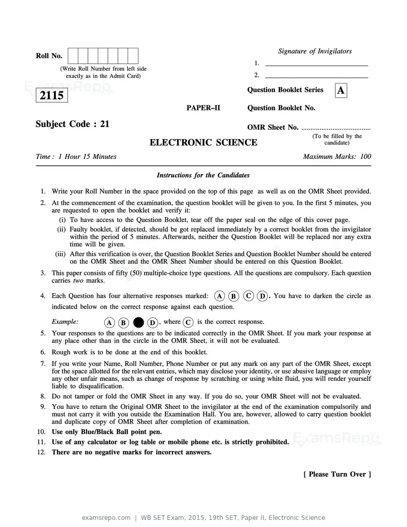
Text of page 1
Signature of Invigilators
Roll No.
                                                                               1. _______________________________
        (Write Roll Number from left side
          exactly as in the Admit Card)                                        2. _______________________________

                                                                           Question Booklet Series              A
 2115
                                                      PAPER–II             Question Booklet No.

Subject Code : 21                                                          OMR Sheet No. ......................................
                                                                                                      (To be filled by the
                                            ELECTRONIC SCIENCE                                            candidate)

Time : 1 Hour 15 Minutes                                                                          Maximum Marks: 100

                                             Instructions for the Candidates

 1. Write your Roll Number in the space provided on the top of this page as well as on the OMR Sheet provided.
 2. At the commencement of the examination, the question booklet will be given to you. In the first 5 minutes, you
    are requested to open the booklet and verify it:
       (i) To have access to the Question Booklet, tear off the paper seal on the edge of this cover page.
      (ii) Faulty booklet, if detected, should be got replaced immediately by a correct booklet from the invigilator
           within the period of 5 minutes. Afterwards, neither the Question Booklet will be replaced nor any extra
           time will be given.
     (iii) After this verification is over, the Question Booklet Series and Question Booklet Number should be entered
           on the OMR Sheet and the OMR Sheet Number should be entered on this Question Booklet.
 3. This paper consists of fifty (50) multiple-choice type questions. All the questions are compulsory. Each question
    carries two marks.

 4. Each Question has four alternative responses marked:         AB        C    D . You have to darken the circle as
     indicated below on the correct response against each question.

     Example:          A B C D , where C is the correct response.
 5. Your responses to the questions are to be indicated correctly in the OMR Sheet. If you mark your response at
    any place other than in the circle in the OMR Sheet, it will not be evaluated.
 6. Rough work is to be done at the end of this booklet.
 7. If you write your Name, Roll Number, Phone Number or put any mark on any part of the OMR Sheet, except
    for the space allotted for the relevant entries, which may disclose your identity, or use abusive language or employ
    any other unfair means, such as change of response by scratching or using white fluid, you will render yourself
    liable to disqualification.
 8. Do not tamper or fold the OMR Sheet in any way. If you do so, your OMR Sheet will not be evaluated.
 9. You have to return the Original OMR Sheet to the invigilator at the end of the examination compulsorily and
    must not carry it with you outside the Examination Hall. You are, however, allowed to carry question booklet
    and duplicate copy of OMR Sheet after completion of examination.
10. Use only Blue/Black Ball point pen.
11. Use of any calculator or log table or mobile phone etc. is strictly prohibited.
12. There are no negative marks for incorrect answers.


                                                                                                  [ Please Turn Over ]
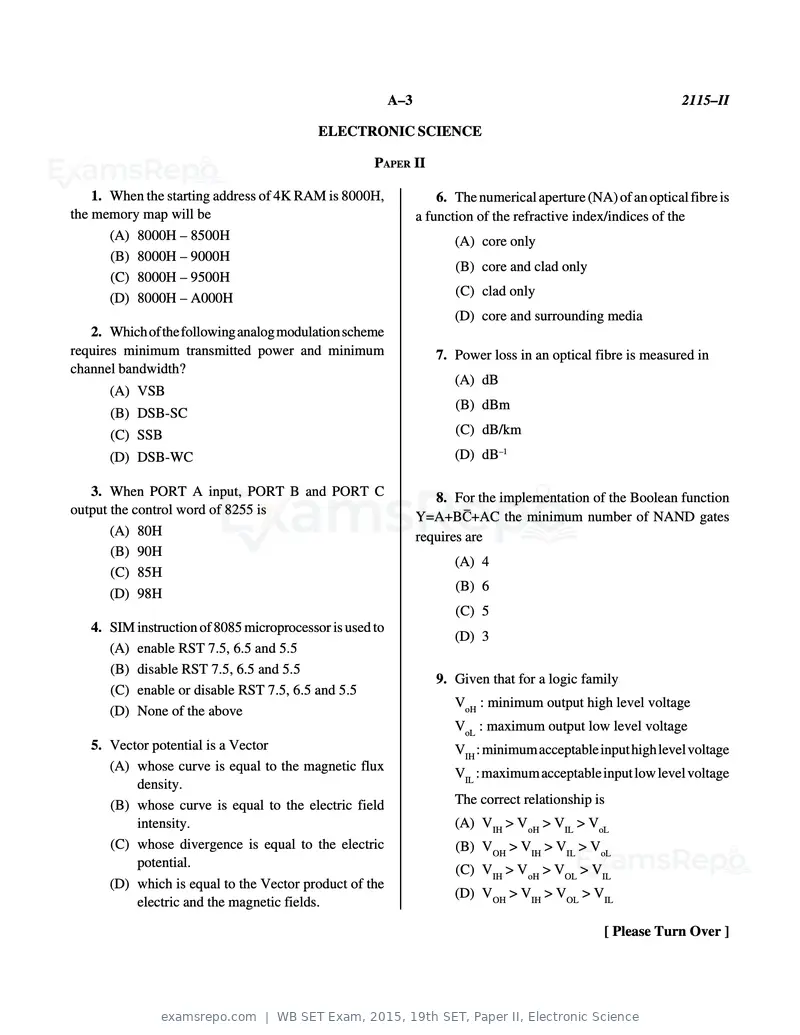
Text of page 3
A–3                                                   2115–II

                                           ELECTRONIC SCIENCE

                                                     PAPER II

    1. When the starting address of 4K RAM is 8000H,                6. The numerical aperture (NA) of an optical fibre is
the memory map will be                                          a function of the refractive index/indices of the
       (A) 8000H – 8500H                                               (A) core only
       (B) 8000H – 9000H
                                                                       (B) core and clad only
       (C) 8000H – 9500H
       (D) 8000H – A000H                                               (C) clad only
                                                                       (D) core and surrounding media
   2. Which of the following analog modulation scheme
requires minimum transmitted power and minimum                     7. Power loss in an optical fibre is measured in
channel bandwidth?
                                                                       (A) dB
      (A) VSB
                                                                       (B) dBm
      (B) DSB-SC
      (C) SSB                                                          (C) dB/km
      (D) DSB-WC                                                       (D) dB–1

   3. When PORT A input, PORT B and PORT C                         8. For the implementation of the Boolean function
output the control word of 8255 is
                                                                Y=A+B¶Òfi+AC the minimum number of NAND gates
       (A) 80H                                                  requires are
       (B) 90H
                                                                       (A) 4
       (C) 85H
                                                                       (B) 6
       (D) 98H
                                                                       (C) 5
   4. SIM instruction of 8085 microprocessor is used to
                                                                       (D) 3
      (A) enable RST 7.5, 6.5 and 5.5
      (B) disable RST 7.5, 6.5 and 5.5
                                                                   9. Given that for a logic family
      (C) enable or disable RST 7.5, 6.5 and 5.5
                                                                       VoH : minimum output high level voltage
      (D) None of the above
                                                                       VoL : maximum output low level voltage
   5. Vector potential is a Vector                                     VIH : minimum acceptable input high level voltage
      (A) whose curve is equal to the magnetic flux                    VIL : maximum acceptable input low level voltage
          density.
      (B) whose curve is equal to the electric field                   The correct relationship is
          intensity.                                                   (A) VIH > VoH > VIL > VoL
      (C) whose divergence is equal to the electric                    (B) VOH > VIH > VIL > VoL
          potential.                                                   (C) VIH > VoH > VOL > VIL
      (D) which is equal to the Vector product of the
                                                                       (D) VOH > VIH > VOL > VIL
          electric and the magnetic fields.

                                                                                                  [ Please Turn Over ]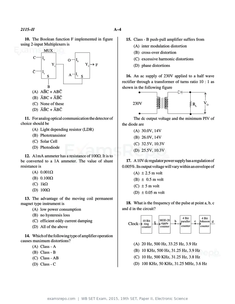
Text of page 4
2115–II A–4
10. The Boolean function F implemented in figure 15. Class - B push-pull amplifier suffers from
using 2-input Multiplexers is (A) inter modulation distortion
MUX
(B) cross-over distortion
C I0 (C) excessive harmonic distortions
O I0
Y1 Y2 F (D) phase distortions
¶Òfi I1
A I1
S S 16. An ac supply of 230V applied to a half wave
rectifier through a transformer of turns ratio 10 : 1 as
B shown in the following figure
(A) A•ÒfiC + AB¶Òfi
(B) §Ò‡BC + §Ò‡•Òfi¶Òfi
(C) None of these
(D) §Ò‡•ÒfiC + §Ò‡B¶Òfi
230V
/ / YR
L
VO
11. For analog optical communication the detector of The dc output voltage and the minimum PIV of
choice should be the diode are
(A) Light depending resistor (LDR) (A) 30.0V, 14V
(B) Phototransistor (B) 26.0V, 14V
(C) Solar Cell
(C) 32.5V, 10.3V
(D) Photodiode
(D) 25.5V, 10.3V
12. A1mA ammeter has a resistance of 100. It is to
be converted to a 1A ammeter. The value of shunt 17. A 10V dc regulator power supply has a regulation of
resistance is 0.005%. Its output voltage will vary within an envelope of
(A) 0.001 (A) 2.5 m volt
(B) 0.100 (B) 0.5 m volt
(C) 1k (C) 5 m volt
(D) 100
(D) 0.05 m volt
13. The advantage of the moving coil permanent
magnet type instrument is 18. What is the frequency of the pulse at point a, b, c
(A) low power consumption and d in the circuit?
(B) no hysteresis loss
4 Bit 4 Bit
(C) efficient eddy current damping 10 Bit a MOD-20 b paraller c Johnson d
Clock ring ripple counter counter
(D) All of the above counter counter
14. Which of the following type of amplifier operation
causes maximum distortions?
(A) 20 Hz, 500 Hz, 33.25 Hz, 3.9 Hz
(A) Class - A
(B) Class - B (B) 10 KHz, 500 Hz, 31.25 Hz, 3.9 Hz
(C) Class - AB (C) 10 Hz, 500 KHz, 31.25 Hz, 3.8 Hz
(D) Class - C (D) 100 KHz, 50 KHz, 31.25 MHz, 3.6 Hz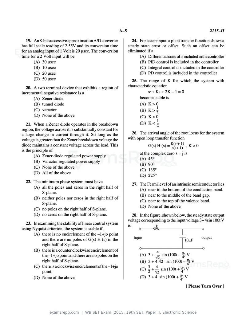
Text of page 5
A–5 2115–II
19. An 8-bit successive approximation A/D converter 24. For a step input, a plant transfer function shows a
has full scale reading of 2.55V and its conversion time steady state error or offset. Such an offset can be
for an analog input of 1 Volt is 20 sec. The conversion eliminated if a
time for a 2 Volt input will be (A) Differential control is included in the controller
(A) 30 sec (B) PID control is included in the controller
(B) 10 sec (C) Integral control is included in the controller
(C) 20 sec (D) PD control is included in the controller
(D) 50 sec 25. The range of K for which the system with
20. A two terminal device that exhibits a region of characteristic equation
incremental negative resistance is a s2 + Ks + 2K – 1 = 0
(A) Zener diode become stable is
(B) tunnel diode (A) K > 0
1
(C) varactor (B) K >
2
(D) None of the above (C) K < 0
1
21. When a Zener diode operates in the breakdown (D) K <
2
region, the voltage across it is substantially constant for
a large change in current through it. So long as the 26. The arrival angle of the root locus for the system
voltage is greater than the Zener breakdown voltage the with open loop transfer function
diode maintains a constant voltage across the load. This K(s2+ 1)
G(s) H (s) = s(s+ 1) , K > 0
is the principle of
at the complex zero s = j is
(A) Zener diode regulated power supply
(A) 45
(B) Varactor regulated power supply
(B) 90
(C) None of the above
(C) 135
(D) All of the above
(D) 225
22. The minimum phase system must have
27. The Fermi level of an intrinsic semiconductor lies
(A) all the poles and zeros in the right half of
(A) near to the bottom of the conduction band.
S-plane.
(B) near to the middle of the band gap.
(B) neither poles nor zeros in the right half of
(C) near to the top of the valence band.
S-plane.
(D) None of the above
(C) no poles on the right half of S-plane.
(D) no zeros on the right half of S-plane. 28. In the figure, shown below, the steady state output
voltage corresponding to the input voltage 3+ 4sin 100t V
23. In examining the stability of linear control system is 1k
using Nyquist criterion, the system is stable if, Y
(A) there is no encirclement of the –1+jo point
input output
and there are no poles of G(s) H (s) in the 10F
right half of S-plane.
(B) there is a counter clockwise encirclement of 4
the –1+jo point and there are no poles on the (A) 3 + sin (100t – 4) V
2
right half of S-plane. (B) 3 + 4 2 sin (100t – ) V
4
(C) there is a clockwise encirclement of the –1+jo 3 4
(C) + sin (100t + ) V
point. 2 2 4
(D) 3 + 4 sin (100t + ) V
(D) None of the above 4
[ Please Turn Over ]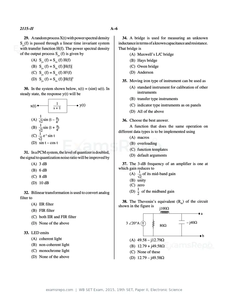
Text of page 6
2115–II A–6
29. A random process X(t) with power spectral density 34. A bridge is used for measuring an unknown
Sys(f) is passed through a linear time invariant system inductance in terms of a known capacitance and resistance.
with transfer function H(f). The power spectral density That bridge is
of the output process Sys (f) is given by (A) Maxwell’s L/C bridge
(A) Sys (f) = Sxs (f) H(f) (B) Hays bridge
(B) Sys (f) = Sxs (f) |H(f)| (C) Owen bridge
(C) Sys (f) = Sxs (f) H2(f) (D) Anderson
(D) Sys (f) = Sxs (f) |H(f)|2 35. Moving iron type of instrument can be used as
30. In the system shown below, x(t) = (sint) u(t). In (A) standard instrument for calibration of other
steady state, the response y(t) will be instruments
(B) transfer type instruments
1 y(t) (C) indicator type instruments as on panels
x(t)
s+1
(D) All of the above
1
(A) 2 sin (t – ) 36. Choose the best answer.
4
1
(B) sin (t + ) A function that does the same operation on
2 4 different data types is to be implemented using
1 –t
(C) e sin t (A) macros
2
(D) sin t – cos t (B) overloading
(C) function templates
31. In a PCM system, the level of quantizer is doubled,
(D) default arguments
the signal to quantization noise ratio will be improved by
(A) 3 dB 37. The 3-dB frequency of an amplifier is one at
(B) 6 dB which gain reduces to
1
(A) of its mid-band gain
(C) 8 dB 2
(B) unity
(D) 10 dB
(C) zero
1
32. Bilinear transformation is used to convert analog (D) of the midband gain
2
filter to
38. The Thevenin’s equivalent (Rth) of the circuit
(A) IIR filter shown in the figure is
j100
(B) FIR filter
(C) both IIR and FIR filter
/ a
Y
(D) None of the above 3 20A – j40
80
33. LED emits
b
(A) coherent light (A) 49.58 – j12.79
(B) non-coherent light (B) 12.79 + j49.58
(C) monochrome light (C) None of these
(D) None of the above (D) 12.79 – j49.58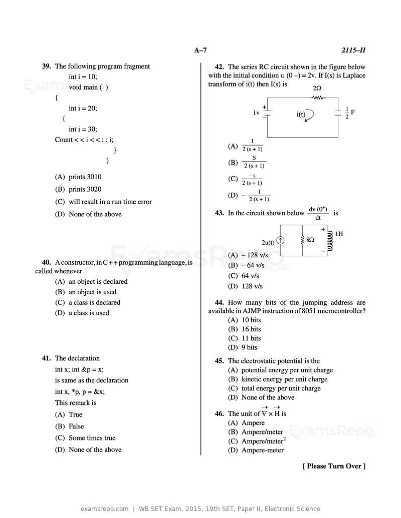
Text of page 7
A–7 2115–II
39. The following program fragment 42. The series RC circuit shown in the figure below
int i = 10; with the initial condition (0 –) = 2v. If I(s) is Laplace
void main ( ) transform of i(t) then I(s) is
2
{ Y
int i = 20; + 1
1v i(t) F
{ – 2
int i = 30;
Count < < i < < : : i; 1
(A) 2 (s + 1)
}
S
} (B) 2 (s + 1)
(A) prints 3010 –s
(C)
2 (s + 1)
(B) prints 3020 1
(D) –
2 (s + 1)
(C) will result in a run time error
dv (0+)
(D) None of the above 43. In the circuit shown below is
dt
+
1H
(A) – 128 v/s
2u(t) Y 8
– /
40. A constructor, in C + + programming language, is (B) – 64 v/s
called whenever
(C) 64 v/s
(A) an object is declared
(D) 128 v/s
(B) an object is used
(C) a class is declared 44. How many bits of the jumping address are
(D) a class is used available in AJMP instruction of 8051 microcontroller?
(A) 10 bits
(B) 16 bits
(C) 11 bits
(D) 9 bits
41. The declaration 45. The electrostatic potential is the
int x; int &p = x; (A) potential energy per unit charge
is same as the declaration (B) kinetic energy per unit charge
int x, *p, p = &x; (C) total energy per unit charge
(D) None of the above
This remark is
(A) True 46. The unit of × H is
(B) False (A) Ampere
(B) Ampere/meter
(C) Some times true (C) Ampere/meter2
(D) None of the above (D) Ampere-meter
[ Please Turn Over ]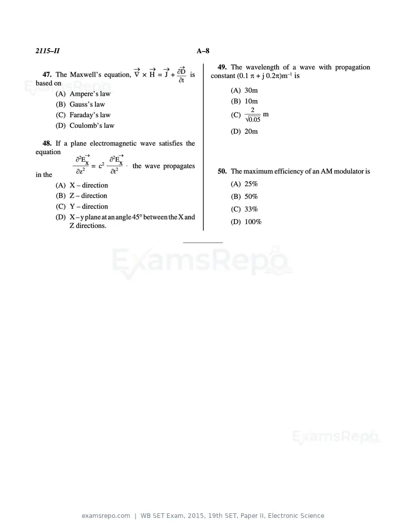
Text of page 8
2115–II A–8
49. The wavelength of a wave with propagation
47. The Maxwell’s equation, × H = J + D is constant (0.1 + j 0.2)m–1 is
based on t
(A) Ampere’s law (A) 30m
(B) Gauss’s law (B) 10m
2
(C) Faraday’s law (C) m
0.05
(D) Coulomb’s law
(D) 20m
48. If a plane electromagnetic wave satisfies the
equation 2
2E
x = c2 Ex , the wave propagates
z2 t2 50. The maximum efficiency of an AM modulator is
in the
(A) X – direction (A) 25%
(B) Z – direction (B) 50%
(C) Y – direction (C) 33%
(D) X – y plane at an angle 45 between the X and
(D) 100%
Z directions.
Text of page 9
A–9       2115–II
ROUGH WORK

Text of page 10
2115–II      A–10

          ROUGH WORK
Text of page 11
A–11      2115–II
ROUGH WORK

Text of page 12
2115–II      A–12

          ROUGH WORK
Official key not published for this paper.
Page 1 of 12
Source: West Bengal College Service Commission. Question paper published by West Bengal College Service Commission.