
MH SET 2011: 7 August, Paper II, Electronic Science

Text of page 1
AUG-38211/II
                         ELECTRONIC SCIENCE
                                   Paper II
Time Allowed : 75 Minutes]                          [Maximum Marks : 100
Note : This Paper contains Fifty (50) multiple choice questions, each question
       carrying Two (2) marks. Attempt All questions.


1.   In a p-n junction, p-type region is       3.   What is the function of SiO2 layer

     heavily doped as a result :                    in MOSFET ?

                                                    (A) To      provide   high   input
     (A) depletion width extends in
                                                        resistance
         n-type region
                                                    (B) To increase current concentra-
     (B) depletion width extends in                     tion
         p-type region                              (C) To provide high output resis-

     (C) depletion width is unaffected                  tance

                                                    (D) To provide low output resis-
     (D) depletion width reduces
                                                        tance
2.   The diffusion process in a p-n
                                               4.   Compared to bipolar junction
     junction device occurs due to :                transistor, a JFET has :

     (A) Ambient temperature                        (A) lower input impedance

     (B) Applied voltage                            (B) higher input impedance and
                                                        high voltage gain
     (C) Covalent bonds
                                                    (C) higher voltage gain
     (D) Concentration gradient of
                                                    (D) high input impedance and low
         charges                                        voltage gain

                                           1                                     [P.T.O.
Text of page 2
AUG-38211/II

                                               7.    The Laplace transform of cosh ωt
5.   Which of the following lithography
                                                     is :
     techniques gives best resolution ?
                                                              s
                                                     (A)
                                                            s + ω2
                                                            2

     (A) UV Lithography
                                                              s
                                                     (B)
                                                            s − ω2
                                                            2

     (B) E-beam Lithography
                                                              ω
                                                     (C)
                                                            s + ω2
                                                            2
     (C) X-ray Lithography
                                                              ω
                                                     (D)
     (D) Laser Lithography                                  s − D2
                                                            2


                                               8.    Show how many poles this network
6.   Superposition theorem is valid only
                                                     has        in   its   driving    point

     for :                                           impedance ?

                                                            R = 5Ω
     (A) linear circuits                             1                               2+


     (B) non-linear circuits                        V1(s)                  L = 2(s) V2(s)

     (C) both linear and non-linear                  1                               2–

             circuits                                (A) Zero

                                                     (B) One at origin
     (D) circuits containing current
                                                     (C) One at infinity
             circuits
                                                     (D) One on jω axis

                                           2
Text of page 3
AUG-38211/II

9.   How   is        z 22       related   to
                                                   11. In a bridge rectifier the secondary
     h-parameters ?
                                                       voltage is 100 V, what should be the
     (A) z22 = h22
                                                       minimum PIV for each diode ?
                1
     (B) z22 = h
                22
                                                       (A) 100 V
               h21
     (C) z22 = h
                22
                                                       (B) 141.4 V
                 h21
     (D) z22 = − h
                     22                                (C) 200 V

10. The pole-zero pattern of a filter is
                                                       (D) 282.8 V
     shown in figure. The filter is :

                                                   12. An amplifier has a voltage gain of
                Jω
                          J2
                                                       AV = 40 and 10% of the output is
                          J1
                                                       fedback. The gain with feedback
                                σ
                                                       is :
                          –J1

                          J2                           (A) 40


                                                       (B) 32
     (A) low pass

     (B) high pass                                     (C) 16
     (C) band pass
                                                       (D) 8
     (D) all pass

                                               3                                    [P.T.O.
Text of page 4
AUG-38211/II

                                              15. Slew rate of op-amp becomes
13. In a CE small signal amplifier, the
                                                    important :
    resistor R E is bypassed by a
                                                    (A) at low frequency
    capacitor CE. The input impedance
                                                    (B) at high frequency
    of this configuration is :
                                                    (C) at low input voltage
    (A) hfe
                                                    (D) at high input voltage

    (B) R E                                   16. The main advantage of CMOS

                                                    is :
    (C) hie + (1 + hfe)RE
                                                    (A) Low power, high device density
    (D) (1 + hfe)RE
                                                    (B) High speed, high device density

14. When a large sine wave drives a
                                                    (C) Low power, low device density

    Schmitt    trigger,   the    output
                                                    (D) High speed, low device density

    is a :                                    17.   Y = ABC + ABC + 1, the output Y

                                                    will be :
    (A) rectangular wave

                                                    (A) zero
    (B) triangular wave
                                                    (B) AB
    (C) rectified sine wave
                                                    (C) 1

    (D) series of ramps                             (D) ABC

                                          4
Text of page 5
AUG-38211/II

18. A CMOS D latch is transparent,         20. An    eightbit     flash   ADC     is

                                               implemented using :
    when :
                                               (A) 8 comparators
    (A) EN = 0
                                               (B) 16 comparators
    (B) EN = 1
                                               (C) 64 comparators

    (C) EN = tristate                          (D) 256 comparators

    (D) Independent of EN                  21. The register used in variable port

                                               addressing in 8086 is :
19. A 64 kB memory device will
                                               (A) AX
    have :
                                               (B) BX
    (A) 16 address lines and 8 data
                                               (C) CX
        lines
                                               (D) DX

    (B) 20 address lines and 4 data
                                           22. Address within a segment of 8086

        lines                                  is called :


    (C) 64 address lines and 8 data            (A) effective address


        lines                                  (B) physical address

                                               (C) segment address
    (D) 16 address lines and 16 data
                                               (D) base address
        lines


                                       5                                     [P.T.O.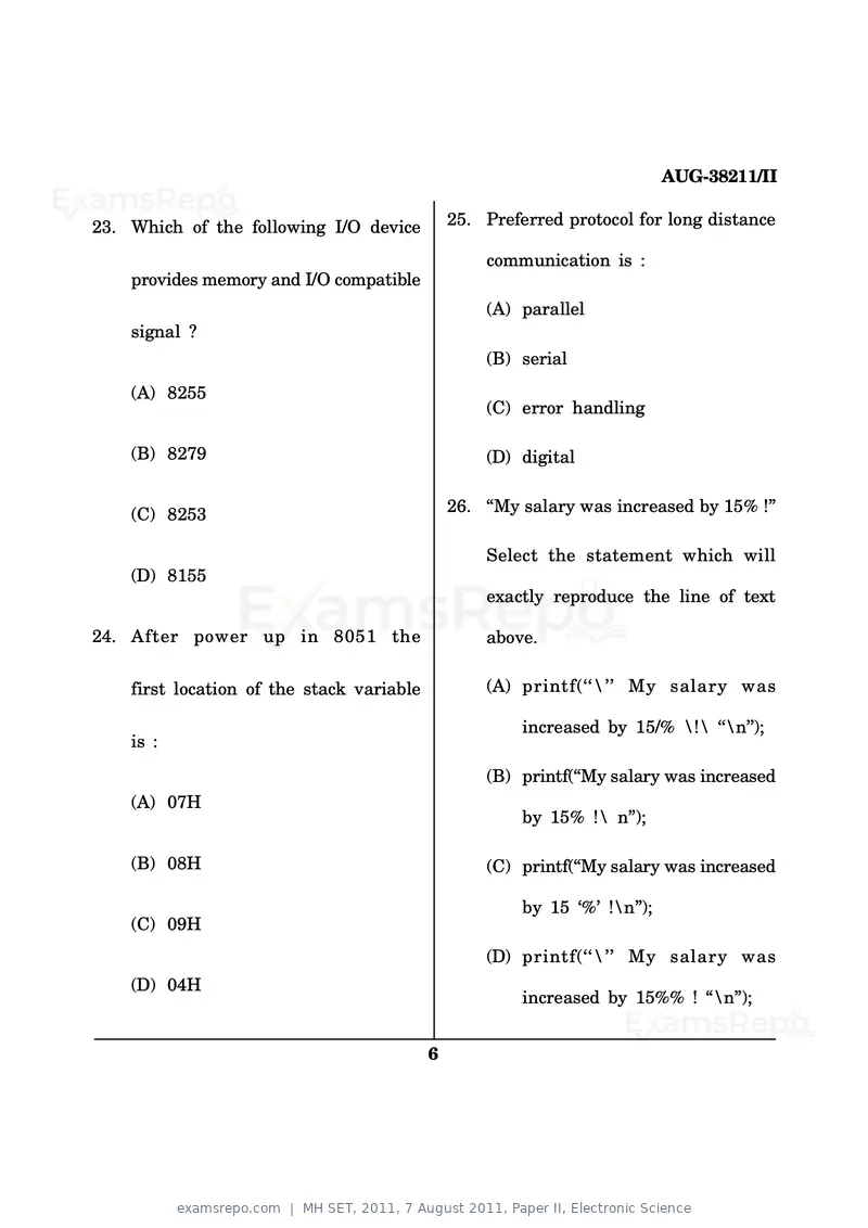
Text of page 6
AUG-38211/II

23. Which of the following I/O device          25. Preferred protocol for long distance

                                                   communication is :
    provides memory and I/O compatible
                                                   (A) parallel
    signal ?
                                                   (B) serial
    (A) 8255
                                                   (C) error handling

    (B) 8279                                       (D) digital


    (C) 8253                                   26. ‘‘My salary was increased by 15% !’’

                                                   Select the statement which will
    (D) 8155
                                                   exactly reproduce the line of text

24. After power up in 8051 the                     above.

    first location of the stack variable           (A) printf(‘‘\’’ My salary was

                                                        increased by 15/% \!\ ‘‘\n’’);
    is :
                                                   (B) printf(‘‘My salary was increased
    (A) 07H
                                                        by 15% !\ n’’);

    (B) 08H                                        (C) printf(‘‘My salary was increased

                                                        by 15 ‘%’ !\n’’);
    (C) 09H
                                                   (D) printf(‘‘\’’ My salary was
    (D) 04H
                                                        increased by 15%% ! “\n’’);


                                           6
Text of page 7
AUG-38211/II
27. int X = 2 * 3 + 4 * 5;
                                                29. Which of the following is the correct
    What value will X contain in the
                                                    way of declaring a float pointer ?
    sample code above ?

    (A) 22                                          (A) float ptr;

    (B) 26
                                                    (B) float * ptr;
    (C) 46
                                                    (C) * float ptr;
    (D) 70

                                                    (D) float ptr*;
28. Array passed as an argument to a

    function is interpreted as :                30. Which one of the following will


    (A) Address of the array                        read a character from keyboard


                                                    and will store it in the variable
    (B) Value of the first element of the

                                                    C ?
        array


    (C) Address of the first element of             (A) C=getc( );


        the array                                   (B) getc(&c);


    (D) Number of elements of the                   (C) C=getchar(stdin);

        array
                                                    (D) C=getchar( );


                                            7                                     [P.T.O.
Text of page 8
AUG-38211/II

31. An electromagnetic wave in a             33. The characteristic impedance of a

    medium with permittivity ∈ and               transmission line is 100 Ω, which is

    permeability µ travels with a                terminated into a load of 900 Ω.
                                                     λ
                                                 A     transformer is to be added for
    speed :                                          4
                                                 matching the impedance. Its
    (A)    ∈µ
                                                 characteristic impedance should
           1
    (B)    ∈µ                                    be :


           ∈                                     (A) 500 Ω
    (C)
           µ
                                                 (B) 700 Ω
           µ
    (D)
           ∈                                     (C) 900 Ω

32. Poynting vector represents :
                                                 (D) 300 Ω

    (A) direction of propagation of EM
                                             34. Increase in number of directors in
          waves
                                                 Yagi antenna :

    (B) direction of displacement
                                                 (A) increases the bandwidth
          current
                                                 (B) decreases the bandwidth
    (C) polarization vector
                                                 (C) decreases the gain
    (D) equipotential surface
                                                 (D) increases null points


                                         8
Text of page 9
AUG-38211/II

    35. When a plane polarized wave is               37. If   10     speech     channels     are

                                                         multiplexed       in   a    TDM-PCM
        incident on a conducting surface, the
                                                         telephone system and the signals
        magnetic field at the interface is :
                                                         are sampled at 8 kHz rate. Then

        (A) zero                                         separation time between two frames

                                                         will be :
        (B) same as in the incident

                                                         (A) 12.5 µ sec.
              wave

                                                         (B) 15.0 µ sec.
        (C) double that of the incident
                                                         (C) 1.25 µ sec.
              wave
                                                         (D) 125 µ sec.
1       (D)        that    of   the   incident
2                                                    38. What makes optical fiber immune to
              wave
                                                         EMI ?

    36. The frequency bandwidth required
                                                         (A) They transmit signal as electric

        is largest for :                                      current rather than light


        (A) amplitude modulation                         (B) It has plastic cover on it

                                                         (C) Because it uses glass or polymer
        (B) frequency modulation
                                                              as propagation medium
        (C) digital modulation
                                                         (D) They transmit signal as light

        (D) FSK modulation                                    rather than electric current


                                                 9                                        [P.T.O.
Text of page 10
AUG-38211/II

39. Microwave link repeaters are
                                                  41. In the reverse direction the
   typically 50 km apart :
                                                      characteristics of a thyristor
   (A) because       of    atmospheric
                                                      resembles to characteristics of a :
       attenuation

   (B) because of earth’s curvature                   (A) transistor switch


   (C) because     of     output   power              (B) p-n rectifier

       limitation of transmitter
                                                      (C) negative resistance
   (D) to ensure that the applied d.c.

       voltage is not excessive                       (D) two transistor model


40. Figure    of   merit     of    digital        42. For a UJT R B1 = 6 kΩ, R B2 = 3 kΩ

   communication system is primarily
                                                      the intrinsic stand-off ratio will
   determined by :
                                                      be :
   (A) SNR and probability Pe
                                                      (A) 0.55
   (B) Bandwidth and signalling rate

       rs                                             (B) 0.33

   (C) Error probability and signalling
                                                      (C) 0.66
       rate
                                                      (D) 0.44
   (D) SNR and bandwidth

                                             10
Text of page 11
AUG-38211/II


                                                 45. Total internal reflection occurs when
43. Stimulated emission is observed in
                                                     light travels from :
    the case of a :
                                                     (A) denser to lighter medium

    (A) Discharge tube
                                                     (B) lighter to denser with incident

                                                          angle > critical angle
    (B) LED

                                                     (C) denser to lighter with incident
    (C) Laser
                                                          angle < critical angle

    (D) Sun                                          (D) lighter to denser medium

                                                 46. Which of the following forms of
44. An illuminated solar cell operates on
                                                     temperature sensor produces a large
    I-V plot with voltage along X-axis
                                                     change in its resistance with

    in the :                                         temperature but is very non-

                                                     linear ?
    (A) 1st
                                                     (A) a thermistor

    (B) 2nd                                          (B) platinum resistance thermo-

                                                          meter
    (C) 3rd
                                                     (C) p-n junction sensor
    (D) 4th quadrant
                                                     (D) pyroelectric sensor


                                            11                                     [P.T.O.
Text of page 12
AUG-38211/II


47. How many significant figures are          49. A system is said to be stable if and

                                                  only if :
    present in the number 10,450 ?

                                                  (A) all poles lie on the right half of
    (A) three
                                                       s-plane

    (B) four                                      (B) all poles lie in the left half of

                                                       s-plane
    (C) five

                                                  (C) all poles and zero lie on the right
    (D) ten
                                                       half of s-plane

48. Which of the following equipments             (D) some poles lie on the right half

    is used to study the topography of                 of s-plane and some lie on the

                                                       left half of s-plane
    the sample ?
                                              50. The problem with PI controller is,
    (A) X-ray Diffractometer
                                                  its response to transients is :

    (B) Spectrophotometer                         (A) very fast

                                                  (B) having a dead zone
    (C) Spectrum Analyser

                                                  (C) non-linear
    (D) Scanning Electron Microscope
                                                  (D) Sluggish

                                         12
Text of page 13
AUG-38211/II
ROUGH WORK


    13             [P.T.O.
Text of page 14
AUG-38211/II

ROUGH WORK


    14
Official key not published for this paper.
Page 1 of 14
Source: Savitribai Phule Pune University. Question paper published by Savitribai Phule Pune University.