
Discussion
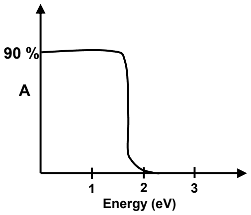
The band gap of a semiconducting material is ~ 2 eV. Which one of the following absorption (A) vs. energy (in eV) curves is correct?
- A.
- B.
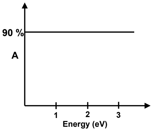
- C.
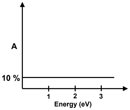
- D.
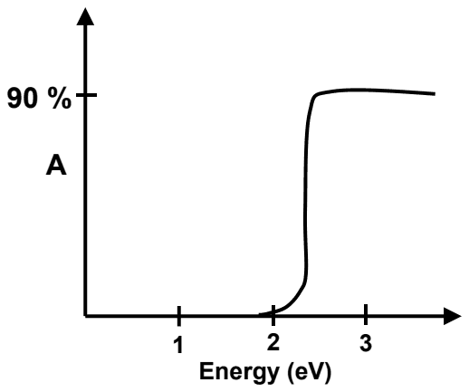
Answer: D
The correct curve is (D).
A photon can be absorbed by exciting an electron across the band gap only if its energy is at least \(E_{g}\). For \(E_{g} \approx 2\) eV, light below about 2 eV passes through with little absorption, and above about 2 eV absorption rises steeply to a high value. That is the step up near 2 eV in curve (D).
Curve (A) is reversed, absorbing low-energy photons and transmitting high-energy ones. The flat curves (B) and (C) show no absorption edge at all, which is how a metal (strong absorption at all energies) or a wide-gap insulator in this range might behave, not a 2 eV semiconductor.
Post your comment
Please log in or register to post a comment.
Examination Categories
- SSC Exams
- Banking Exams
- Teaching Exams
- Civil Services Exams
- Railways Exams
- Engineering Recruitment Exams
- Defence Exams
- State Government Exams
- Police Exams
- Insurance Exams
- Nursing Exams
- Other Government Exams
- NRA CET
- PG Entrance Exams
- Campus Placement
- MBA Entrance Exams
- CUET and UG Entrance
- Judiciary Exams
- Regulatory Body Exams
- Software Development