
Discussion
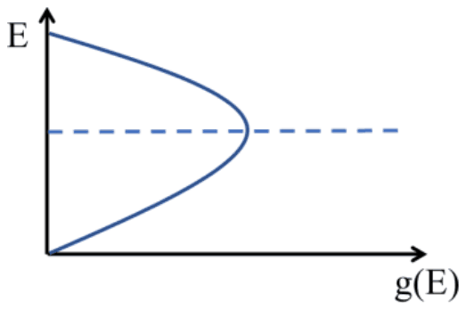
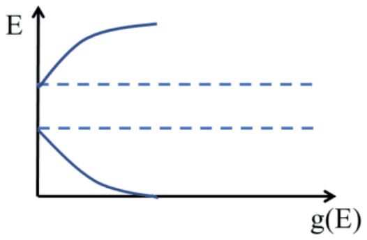
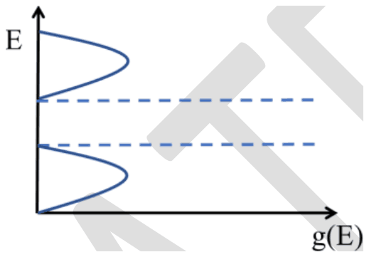
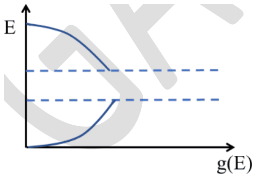
Which one of the following figures corresponds to the density of states g(E) of a typical intrinsic semiconductor? (E represents the energy level of a charge carrier)
- A.
- B.
- C.
- D.
Answer: C
The correct figure is (C).
An intrinsic semiconductor has a filled valence band and an empty conduction band separated by a gap with no allowed states, so the plot must show two bands with a gap. Near each band edge the density of states is proportional to \(\sqrt{E - E_{edge}}\), so \(E - E_{edge} \propto g^{2}\): plotted with E up and g(E) across, each curve leaves the edge with a horizontal tangent and then bends towards the vertical. Each band is finite, so g(E) rises to a maximum and returns to zero at the other edge, which gives the two separate lobes of (C).
(A) has one continuous band and no gap (a metal-like picture). (D) shows the two bands overlapping, which has no gap. (B) does have a gap, but its curves leave the axis steeply (the wrong curvature for a square-root edge) and have no upper limit to the band, so it is not the usual picture.
Post your comment
Please log in or register to post a comment.
Examination Categories
- SSC Exams
- Banking Exams
- Teaching Exams
- Civil Services Exams
- Railways Exams
- Engineering Recruitment Exams
- Defence Exams
- State Government Exams
- Police Exams
- Insurance Exams
- Nursing Exams
- Other Government Exams
- NRA CET
- PG Entrance Exams
- Campus Placement
- MBA Entrance Exams
- CUET and UG Entrance
- Judiciary Exams
- Regulatory Body Exams
- Software Development