
Discussion
A 4 kilobyte (KB) byte-addressable memory is realized using four 1 KB memory blocks. Two input address lines (IA4 and IA3) are connected to the chip select (CS) port of these memory blocks through a decoder as shown in the figure. The remaining ten input address lines from IA11-IA0 are connected to the address port of these blocks. The chip select (CS) is active high.
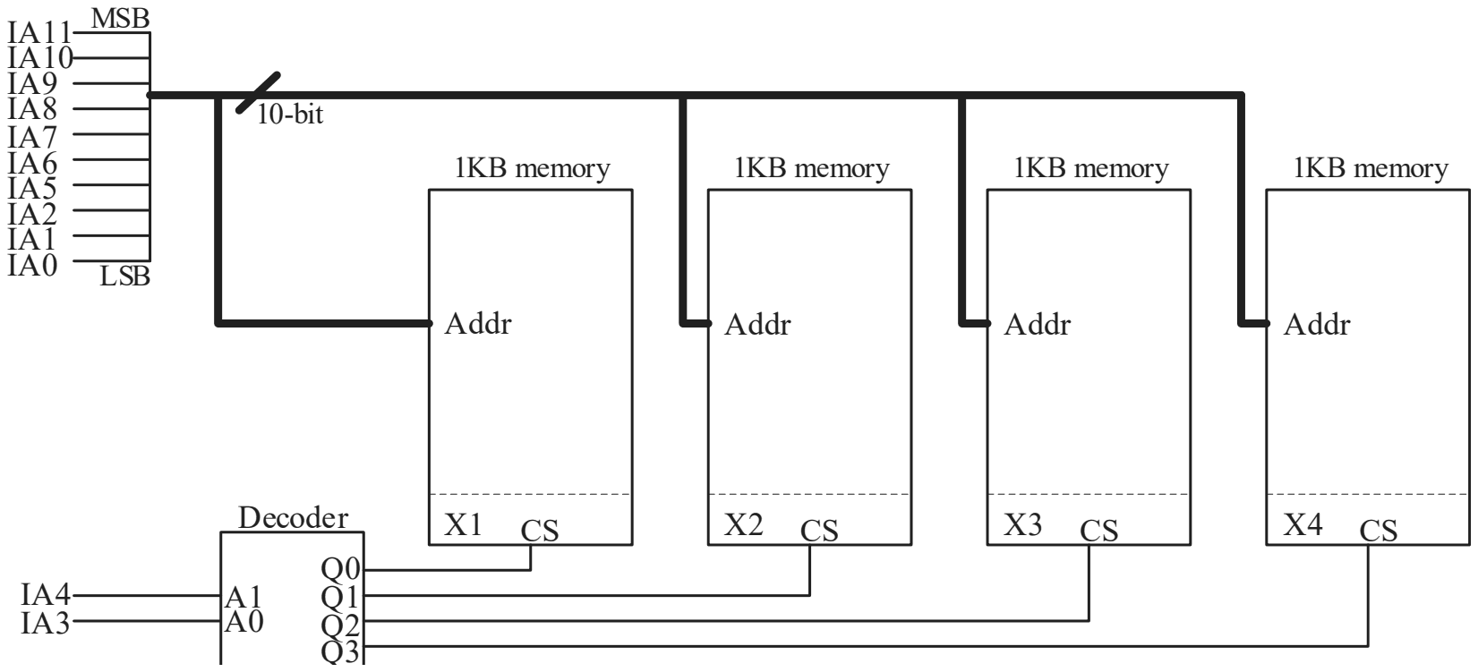
The input memory addresses (IA11-IA0), in decimal, for the starting locations (Addr=0) of each block (indicated as X1, X2, X3, X4 in the figure) are among the options given below. Which one of the following options is CORRECT?
Answer: C
The starting addresses are (0, 8, 16, 24).
Each block is selected by IA4 and IA3 through the decoder: IA4 IA3 = 00 enables X1, 01 enables X2, 10 enables X3 and 11 enables X4. The other ten lines (IA11 to IA5 and IA2 to IA0) form the address inside the block. The starting location of a block, Addr = 0, has all ten of those lines at 0, so only IA4 and IA3 can be 1:
\[ \begin{aligned} X1&: 0,\quad X2: 2^{3} = 8 \\ X3&: 2^{4} = 16,\quad X4: 2^{4} + 2^{3} = 24 \end{aligned} \]
(0, 1024, 2048, 3072) is what the usual design gives, with the two top lines IA11 and IA10 on the decoder; here the decoder sits on bits 4 and 3. (0, 1, 2, 3) would need IA1 and IA0 on the decoder. The four blocks cannot all start at address 0, because each address enables exactly one block.
Post your comment
Please log in or register to post a comment.
Examination Categories
- SSC Exams
- Banking Exams
- Teaching Exams
- Civil Services Exams
- Railways Exams
- Engineering Recruitment Exams
- Defence Exams
- State Government Exams
- Police Exams
- Insurance Exams
- Nursing Exams
- Other Government Exams
- NRA CET
- PG Entrance Exams
- Campus Placement
- MBA Entrance Exams
- CUET and UG Entrance
- Judiciary Exams
- Regulatory Body Exams
- Software Development