
GATE EC 2013: Electronics and Communication Engineering

Text of page 1
SESSION - 1
Text of page 2
2013                                                                      Question Booklet Code
                                                                                                         A
         EC : ELECTRONICS AND COMMUNICATION ENGINEERING
Duration: Three Hours                                                                     Maximum Marks: 100

Read the following instructions carefully.

    1. Do not open the seal of the Question Booklet until you are asked to do so by the invigilator.
    2. Take out the Optical Response Sheet (ORS) from this Question Booklet without breaking the seal
        and read the instructions printed on the ORS carefully. If you find that either:
        a. The Question Booklet Code printed at the right hand top corner of this page does not match with
             the Question Booklet Code at the right hand top corner of the ORS or
        b. The Question Paper Code preceding the Registration number on the ORS is not EC,
       then exchange the booklet immediately with a new sealed Question Booklet.
    3. On the right hand side of the ORS, using ONLY a black ink ballpoint pen, (i) darken the appropriate
       bubble under each digit of your registration number and (ii) write your registration number, your
       name and name of the examination centre and put your signature at the specified location.
    4. This Question Booklet contains 24 pages including blank pages for rough work. After you are
       permitted to open the seal, check all pages and report discrepancies, if any, to the invigilator.
    5. There are a total of 65 questions carrying 100 marks. All these questions are of objective type. Each
       question has only one correct answer. Questions must be answered on the left hand side of the ORS
       by darkening the appropriate bubble (marked A, B, C, D) using ONLY a black ink ballpoint pen
       against the question number. For each question darken the bubble of the correct answer. More
       than one answer bubbled against a question will be treated as an incorrect response.
    6. Since bubbles darkened by the black ink ballpoint pen cannot be erased, candidates should darken the
       bubbles in the ORS very carefully.
    7. Questions Q.1 – Q.25 carry 1 mark each. Questions Q.26 – Q.55 carry 2 marks each. The 2 marks
       questions include two pairs of common data questions and two pairs of linked answer questions. The
       answer to the second question of the linked answer questions depends on the answer to the first
       question of the pair. If the first question in the linked pair is wrongly answered or is not attempted,
       then the answer to the second question in the pair will not be evaluated.
    8. Questions Q.56 – Q.65 belong to General Aptitude (GA) section and carry a total of 15 marks.
       Questions Q.56 – Q.60 carry 1 mark each, and questions Q.61 – Q.65 carry 2 marks each.
    9. Questions not attempted will result in zero mark and wrong answers will result in NEGATIVE
       marks. For all 1 mark questions, ⅓ mark will be deducted for each wrong answer. For all 2 marks
       questions, ⅔ mark will be deducted for each wrong answer. However, in the case of the linked
       answer question pair, there will be negative marks only for wrong answer to the first question and no
       negative marks for wrong answer to the second question.
    10. Calculator is allowed whereas charts, graph sheets or tables are NOT allowed in the examination hall.
    11. Rough work can be done on the Question Booklet itself. Blank pages are provided at the end of the
        Question Booklet for rough work.
    12. Before the start of the examination, write your name and registration number in the space provided
        below using a black ink ballpoint pen.

           Name

           Registration Number         EC

EC-A                                                                                                      1/24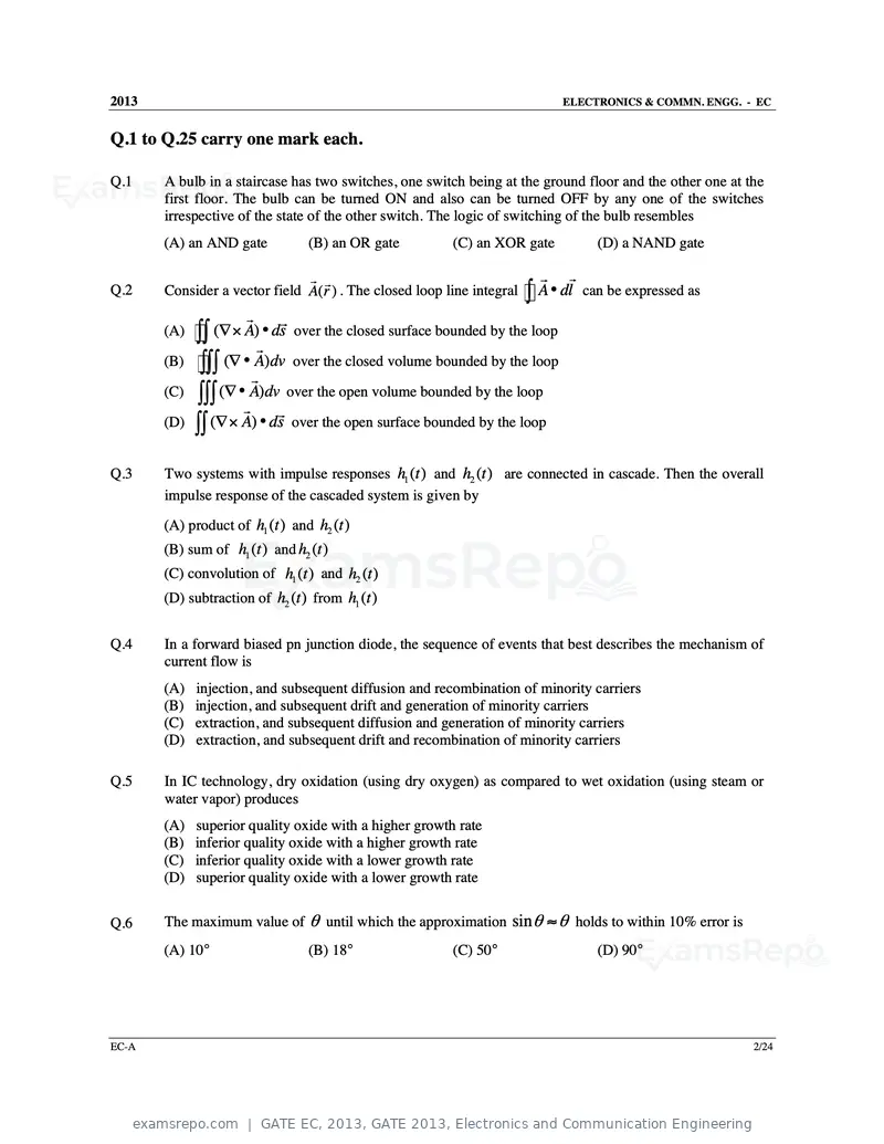
Text of page 3
2013                                                                         ELECTRONICS & COMMN. ENGG. - EC


Q.1 to Q.25 carry one mark each.

Q.1    A bulb in a staircase has two switches, one switch being at the ground floor and the other one at the
       first floor. The bulb can be turned ON and also can be turned OFF by any one of the switches
       irrespective of the state of the other switch. The logic of switching of the bulb resembles
       (A) an AND gate           (B) an OR gate          (C) an XOR gate          (D) a NAND gate

                               r r                                       r r
Q.2    Consider a vector field A( r ) . The closed loop line integral   ∫ • dl can be expressed as
                                                                         A
                   r      r
       (A) ∫∫  (∇× A ) • ds over the closed surface bounded by the loop
                      r
       (B) ∫∫∫ (∇ • A)dv over the closed volume bounded by the loop
                     r
       (C) ∫∫∫ (∇ • A)dv over the open volume bounded by the loop
                   r      r
       (D) ∫∫ (∇ × A) • ds over the open surface bounded by the loop


Q.3    Two systems with impulse responses h1 (t ) and h2 (t ) are connected in cascade. Then the overall
       impulse response of the cascaded system is given by
       (A) product of h1 (t ) and h2 (t )
       (B) sum of h1 (t ) and h2 (t )
       (C) convolution of h1 (t ) and h2 (t )
       (D) subtraction of h2 (t ) from h1 (t )


Q.4    In a forward biased pn junction diode, the sequence of events that best describes the mechanism of
       current flow is
       (A)   injection, and subsequent diffusion and recombination of minority carriers
       (B)   injection, and subsequent drift and generation of minority carriers
       (C)   extraction, and subsequent diffusion and generation of minority carriers
       (D)   extraction, and subsequent drift and recombination of minority carriers

Q.5    In IC technology, dry oxidation (using dry oxygen) as compared to wet oxidation (using steam or
       water vapor) produces
       (A)   superior quality oxide with a higher growth rate
       (B)   inferior quality oxide with a higher growth rate
       (C)   inferior quality oxide with a lower growth rate
       (D)   superior quality oxide with a lower growth rate


Q.6    The maximum value of θ until which the approximation sin θ ≈ θ holds to within 10% error is
       (A) 10°                   (B) 18°                 (C) 50°                  (D) 90°


EC-A                                                                                                      2/24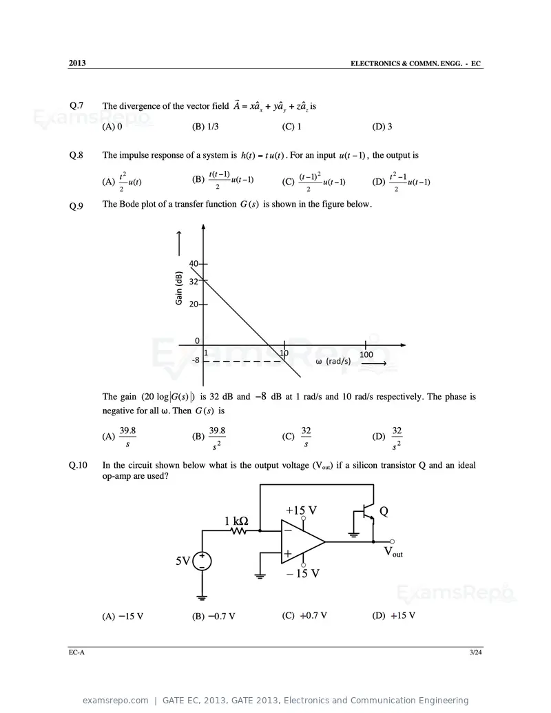
Text of page 4
2013                                                                                            ELECTRONICS & COMMN. ENGG. - EC


                                                          r
Q.7    The divergence of the vector field A = xaˆ x + yaˆ y + zaˆ z is

       (A) 0                            (B) 1/3                     (C) 1                            (D) 3


Q.8    The impulse response of a system is h(t ) = t u (t ) . For an input u (t − 1) , the output is

             t2                               t (t −1)                    (t −1) 2                         t 2 −1
       (A)        u (t )                (B)              u (t −1)   (C)              u (t −1)        (D)            u (t −1)
             2                                  2                           2                                2

Q.9    The Bode plot of a transfer function G (s ) is shown in the figure below.


                            Gain (dB)


       The gain (20 log G ( s) ) is 32 dB and −8 dB at 1 rad/s and 10 rad/s respectively. The phase is
       negative for all ω. Then G (s) is

             39.8                             39.8                        32                                 32
       (A)                              (B)                         (C)                              (D)
              s                                s   2                       s                                 s2
Q.10   In the circuit shown below what is the output voltage (Vout) if a silicon transistor Q and an ideal
       op-amp are used?


                                                                     +15 V                            Q
                                                       1 kΩ
                                                                    –
                                                                    +                                  Vout
                            5V
                                                                     – 15 V


       (A)       15 V                   (B)     0.7 V               (C)     0.7 V                    (D)      15 V


EC-A                                                                                                                           3/24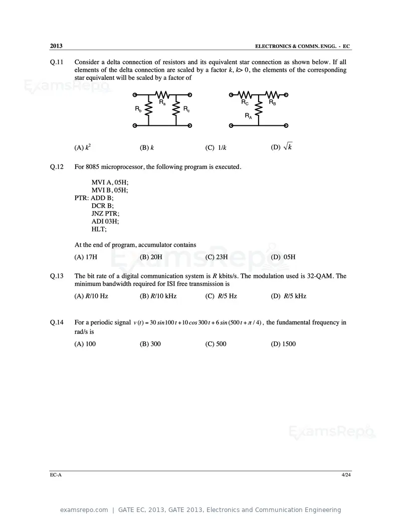
Text of page 5
2013                                                                              ELECTRONICS & COMMN. ENGG. - EC


Q.11   Consider a delta connection of resistors and its equivalent star connection as shown below. If all
       elements of the delta connection are scaled by a factor k, k> 0, the elements of the corresponding
       star equivalent will be scaled by a factor of


                                          Ra                                RC         RB
                                Rb                  Rc
                                                                             RA


       (A) k2                     (B) k                      (C) 1/k                    (D)    k

Q.12   For 8085 microprocessor, the following program is executed.

            MVI A, 05H;
            MVI B, 05H;
       PTR: ADD B;
            DCR B;
            JNZ PTR;
            ADI 03H;
            HLT;

       At the end of program, accumulator contains
       (A) 17H                    (B) 20H                    (C) 23H                    (D) 05H

Q.13   The bit rate of a digital communication system is R kbits/s. The modulation used is 32-QAM. The
       minimum bandwidth required for ISI free transmission is
       (A) R/10 Hz                (B) R/10 kHz               (C) R/5 Hz                 (D) R/5 kHz


Q.14   For a periodic signal v (t ) = 30 sin 100 t + 10 cos 300 t + 6 sin (500 t + π / 4) , the fundamental frequency in
       rad/s is
       (A) 100                    (B) 300                    (C) 500                    (D) 1500


EC-A                                                                                                                  4/24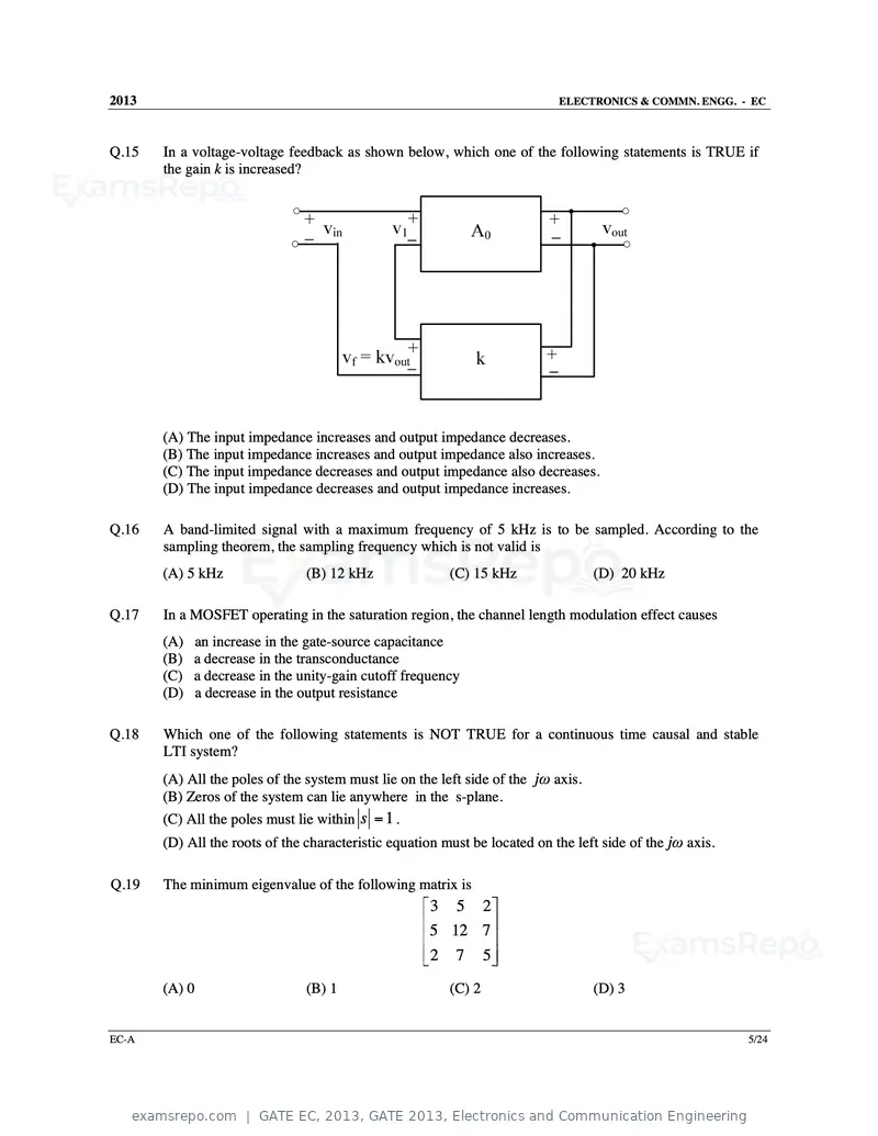
Text of page 6
2013 ELECTRONICS & COMMN. ENGG. - EC
Q.15 In a voltage-voltage feedback as shown below, which one of the following statements is TRUE if
the gain k is increased?
(A) The input impedance increases and output impedance decreases.
(B) The input impedance increases and output impedance also increases.
(C) The input impedance decreases and output impedance also decreases.
(D) The input impedance decreases and output impedance increases.
Q.16 A band-limited signal with a maximum frequency of 5 kHz is to be sampled. According to the
sampling theorem, the sampling frequency which is not valid is
(A) 5 kHz (B) 12 kHz (C) 15 kHz (D) 20 kHz
Q.17 In a MOSFET operating in the saturation region, the channel length modulation effect causes
(A) an increase in the gate-source capacitance
(B) a decrease in the transconductance
(C) a decrease in the unity-gain cutoff frequency
(D) a decrease in the output resistance
Q.18 Which one of the following statements is NOT TRUE for a continuous time causal and stable
LTI system?
(A) All the poles of the system must lie on the left side of the jω axis.
(B) Zeros of the system can lie anywhere in the s-plane.
(C) All the poles must lie within s = 1 .
(D) All the roots of the characteristic equation must be located on the left side of the jω axis.
Q.19 The minimum eigenvalue of the following matrix is
3 5 2
5 12 7
2 7 5
(A) 0 (B) 1 (C) 2 (D) 3
EC-A 5/24
Text of page 7
2013                                                                           ELECTRONICS & COMMN. ENGG. - EC


       A polynomial f ( x) = a4 x + a3 x + a2 x + a1 x − a0 with all coefficients positive has
                                      4       3       2
Q.20

       (A) no real roots                                     (B) no negative real root
       (C) odd number of real roots                          (D) at least one positive and one negative real root


Q.21   Assuming zero initial condition, the response y (t ) of the system given below to a unit step input
       u (t ) is


                                                                  2
       (A) u (t )                  (B) t u (t )              (C) t u (t )
                                                                    2
                                                                                     (D) e − t u (t )


                                 V2 ( s )
Q.22   The transfer function              of the circuit shown below is
                                 V1 ( s )


           0.5 s + 1                                             3s + 6
       (A)                                                   (B)
             s +1                                                 s+2
           s+2                                                   s +1
       (C)                                                   (D)
           s +1                                                  s+2


Q.23   A source vs (t ) = V cos100 π t has an internal impedance of (4 + j3) Ω. If a purely resistive load
       connected to this source has to extract the maximum power out of the source, its value in Ω should be
       (A) 3                       (B) 4                     (C) 5                   (D) 7

Q.24   The return loss of a device is found to be 20 dB. The voltage standing wave ratio (VSWR) and
       magnitude of reflection coefficient are respectively
       (A) 1.22 and 0.1            (B) 0.81 and 0.1          (C) − 1.22 and 0.1      (D) 2.44 and 0.2

                        − π t2
Q.25   Let g (t ) = e    , and h (t ) is a filter matched to g (t ) . If g (t ) is applied as input to h (t ) , then
       the Fourier transform of the output is

                                                             (C) e −π | f |
                                             2                                                     2

       (A) e −π f                  (B) e−π f /2                                      (D) e−2π f
                    2


EC-A                                                                                                              6/24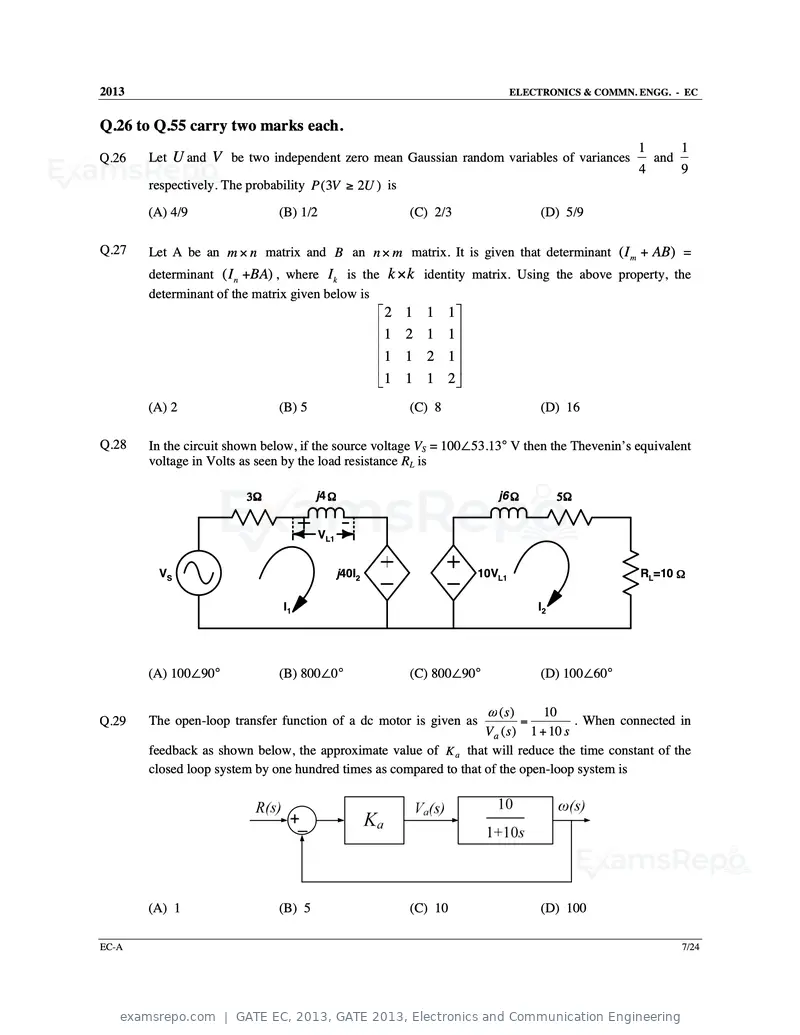
Text of page 8
2013 ELECTRONICS & COMMN. ENGG. - EC
Q.26 to Q.55 carry two marks each.
1 1
Q.26 Let U and V be two independent zero mean Gaussian random variables of variances and
4 9
respectively. The probability P (3V ≥ 2U ) is
(A) 4/9 (B) 1/2 (C) 2/3 (D) 5/9
Q.27 Let A be an m × n matrix and B an n × m matrix. It is given that determinant ( I m + AB ) =
determinant ( I n +BA) , where I k is the k × k identity matrix. Using the above property, the
determinant of the matrix given below is
2 1 1 1
1 2 1 1
1 1 2 1
1 1 1 2
(A) 2 (B) 5 (C) 8 (D) 16
Q.28 In the circuit shown below, if the source voltage VS = 100∠53.13° V then the Thevenin’s equivalent
voltage in Volts as seen by the load resistance RL is
3Ω j4 Ω j6 Ω 5Ω
VL1
VS j40I2 10VL1 RL=10 Ω
I1 I2
(A) 100∠90° (B) 800∠0° (C) 800∠90° (D) 100∠60°
ω (s)10
Q.29 The open-loop transfer function of a dc motor is given as = . When connected in
V a ( s ) 1 + 10 s
feedback as shown below, the approximate value of K a that will reduce the time constant of the
closed loop system by one hundred times as compared to that of the open-loop system is
(A) 1 (B) 5 (C) 10 (D) 100
EC-A 7/24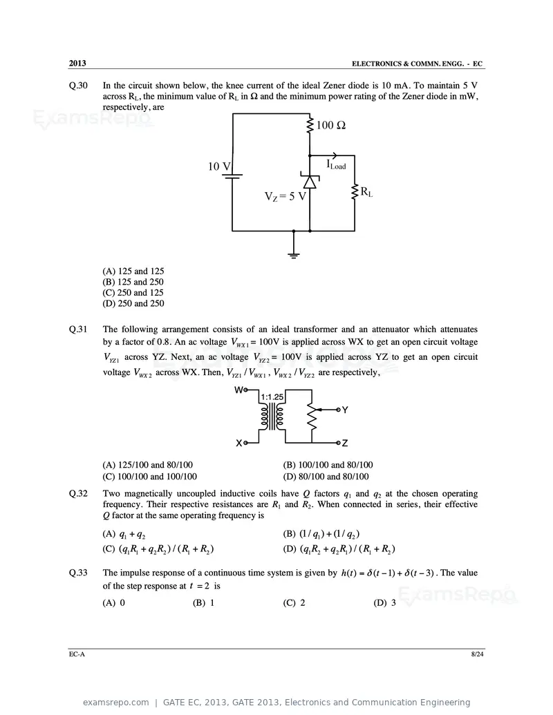
Text of page 9
2013                                                                           ELECTRONICS & COMMN. ENGG. - EC


Q.30   In the circuit shown below, the knee current of the ideal Zener diode is 10 mA. To maintain 5 V
       across RL, the minimum value of RL in Ω and the minimum power rating of the Zener diode in mW,
       respectively, are


       (A) 125 and 125
       (B) 125 and 250
       (C) 250 and 125
       (D) 250 and 250

Q.31   The following arrangement consists of an ideal transformer and an attenuator which attenuates
       by a factor of 0.8. An ac voltage VWX 1 = 100V is applied across WX to get an open circuit voltage
       VYZ 1 across YZ. Next, an ac voltage VYZ 2 = 100V is applied across YZ to get an open circuit
       voltage VWX 2 across WX. Then, VYZ 1 / VWX 1 , VWX 2 / VYZ 2 are respectively,
                                             W
                                                  1:1.25
                                                                           Y


                                             X                             Z

       (A) 125/100 and 80/100                           (B) 100/100 and 80/100
       (C) 100/100 and 100/100                          (D) 80/100 and 80/100
Q.32   Two magnetically uncoupled inductive coils have Q factors q1 and q2 at the chosen operating
       frequency. Their respective resistances are R1 and R2. When connected in series, their effective
       Q factor at the same operating frequency is
       (A) q1 + q2                                      (B) (1 / q1 ) + (1 / q2 )
       (C) ( q1 R1 + q2 R2 ) / ( R1 + R2 )              (D) ( q1 R2 + q2 R1 ) / ( R1 + R2 )

Q.33   The impulse response of a continuous time system is given by h (t ) = δ (t − 1) + δ (t − 3) . The value
       of the step response at t = 2 is
       (A) 0                       (B) 1                (C) 2                       (D) 3


EC-A                                                                                                        8/24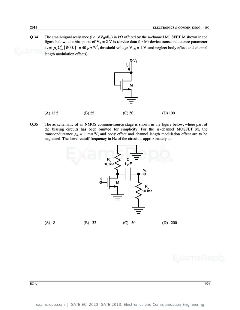
Text of page 10
2013                                                                            ELECTRONICS & COMMN. ENGG. - EC


Q.34   The small-signal resistance (i.e., dVB/dID) in kΩ offered by the n-channel MOSFET M shown in the
       figure below, at a bias point of VB = 2 V is (device data for M: device transconductance parameter
       kN = µn C ′ox (W L ) = 40 µA/V2, threshold voltage VTN = 1 V, and neglect body effect and channel
       length modulation effects)
                                                                   VB
                                                          ID


                                                               M


       (A) 12.5               (B) 25                     (C) 50                      (D) 100

Q.35   The ac schematic of an NMOS common-source stage is shown in the figure below, where part of
       the biasing circuits has been omitted for simplicity. For the n -channel MOSFET M, the
       transconductance gm = 1 mA/V, and body effect and channel length modulation effect are to be
       neglected. The lower cutoff frequency in Hz of the circuit is approximately at


                                              RD          C
                                             10 kΩ       1 µF
                                                                        v0

                                        vi
                                                     M
                                                                         RL
                                                                        10 kΩ


       (A) 8                  (B) 32                     (C) 50                      (D) 200


EC-A                                                                                                        9/24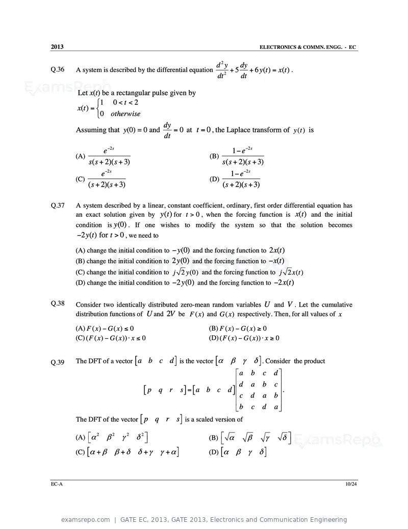
Text of page 11
2013 ELECTRONICS & COMMN. ENGG. - EC
d2y dy
Q.36 A system is described by the differential equation 2
+ 5 + 6 y (t ) = x(t ) .
dt dt
Let x(t) be a rectangular pulse given by
1 0 < t < 2
x (t ) =
0 otherwise
dy
Assuming that y(0) = 0 and = 0 at t = 0 , the Laplace transform of y ( t ) is
dt
e−2 s 1 − e−2 s
(A) (B)
s ( s + 2)( s + 3) s ( s + 2)( s + 3)
e−2s 1 − e−2 s
(C) (D)
(s + 2)(s + 3) (s + 2)(s + 3)
Q.37 A system described by a linear, constant coefficient, ordinary, first order differential equation has
an exact solution given by y (t ) for t > 0 , when the forcing function is x(t ) and the initial
condition is y (0) . If one wishes to modify the system so that the solution becomes
−2 y(t ) for t > 0 , we need to
(A) change the initial condition to − y(0) and the forcing function to 2 x(t )
(B) change the initial condition to 2 y (0) and the forcing function to − x(t )
(C) change the initial condition to j 2 y (0) and the forcing function to j 2 x ( t )
(D) change the initial condition to −2 y (0) and the forcing function to −2 x(t )
Q.38 Consider two identically distributed zero-mean random variables U and V . Let the cumulative
distribution functions of U and 2V be F ( x ) and G ( x ) respectively. Then, for all values of x
(A) F ( x ) − G ( x ) ≤ 0 (B) F ( x ) − G ( x ) ≥ 0
(C) ( F ( x ) − G ( x )) ⋅ x ≤ 0 (D) ( F ( x ) − G ( x )) ⋅ x ≥ 0
Q.39 The DFT of a vector [ a b c d ] is the vector [α β γ δ ] . Consider the product
a b c d
d a b c
[p q r s] = [a b c d ]
c
.
d a b
b c d a
The DFT of the vector [ p q r s ] is a scaled version of
(A) α 2 β 2 γ 2 δ 2 (B) α β γ δ
(C) [α + β β + δ δ + γ γ + α ] (D) [α β γ δ]
EC-A 10/24
Text of page 12
2013                                                                          ELECTRONICS & COMMN. ENGG. - EC


                                                                                    Y (s)
Q.40   The signal flow graph for a system is given below. The transfer function            for this system is
                                                                                    U ( s)


                    s +1                                           s +1
       (A)                                             (B)
             5s + 6s + 2
                2
                                                             s + 6s + 2
                                                               2

               s +1                                               1
       (C)                                             (D)
             s2 + 4 s + 2                                      5s2 + 6s + 2

Q.41   In the circuit shown below the op-amps are ideal. Then Vout in Volts is


       (A) 4                   (B) 6                   (C) 8                       (D) 10
Q.42   In the circuit shown below, Q1 has negligible collector-to-emitter saturation voltage and the diode
       drops negligible voltage across it under forward bias. If Vcc is +5 V, X and Y are digital signals
       with 0 V as logic 0 and Vcc as logic 1, then the Boolean expression for Z is


       (A) X Y                 (B) X Y                 (C) X Y                     (D) XY
EC-A                                                                                                            11/24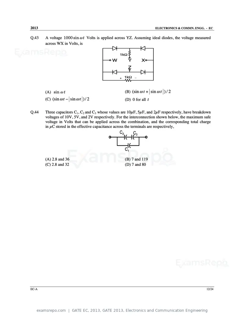
Text of page 13
2013                                                                    ELECTRONICS & COMMN. ENGG. - EC


Q.43   A voltage 1000 sin ω t Volts is applied across YZ. Assuming ideal diodes, the voltage measured
       across WX in Volts, is

                                                 1kΩ
                                             W         Y         X
                                                       Z

                                                 +    1kΩ   _


       (A) sin ω t                                    (B) (sin ω t + sin ω t ) / 2
       (C) (sin ω t − sin ω t ) / 2                   (D) 0 for all t


Q.44   Three capacitors C1, C2 and C3 whose values are 10µF, 5µF, and 2µF respectively, have breakdown
       voltages of 10V, 5V, and 2V respectively. For the interconnection shown below, the maximum safe
       voltage in Volts that can be applied across the combination, and the corresponding total charge
       in µC stored in the effective capacitance across the terminals are respectively,
                                                 C2         C3


                                                      C1

       (A) 2.8 and 36                                 (B) 7 and 119
       (C) 2.8 and 32                                 (D) 7 and 80


EC-A                                                                                               12/24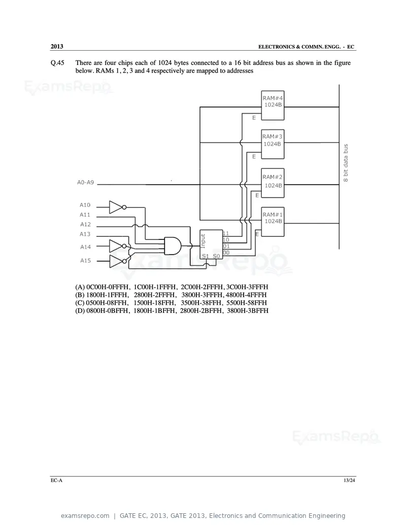
Text of page 14
2013                                                                  ELECTRONICS & COMMN. ENGG. - EC


Q.45   There are four chips each of 1024 bytes connected to a 16 bit address bus as shown in the figure
       below. RAMs 1, 2, 3 and 4 respectively are mapped to addresses


       (A) 0C00H-0FFFH, 1C00H-1FFFH, 2C00H-2FFFH, 3C00H-3FFFH
       (B) 1800H-1FFFH, 2800H-2FFFH, 3800H-3FFFH, 4800H-4FFFH
       (C) 0500H-08FFH, 1500H-18FFH, 3500H-38FFH, 5500H-58FFH
       (D) 0800H-0BFFH, 1800H-1BFFH, 2800H-2BFFH, 3800H-3BFFH


EC-A                                                                                                13/24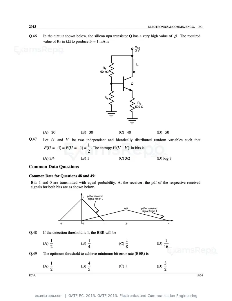
Text of page 15
2013                                                                                       ELECTRONICS & COMMN. ENGG. - EC


Q.46    In the circuit shown below, the silicon npn transistor Q has a very high value of β . The required
        value of R2 in kΩ to produce IC = 1 mA is
                                                                               VCC
                                                                               3V


                                                                               IC
                                                    R1
                                                   60 kΩ


                                                                           Q


                                                          R2
                                                                                RE
                                                                               500 Ω


        (A) 20                  (B) 30                         (C) 40                                (D) 50
Q.47    Let U and V be two independent and identically distributed random variables such that
                                1
         P(U = +1) = P(U = −1) = . The entropy H (U + V ) in bits is
                                2
        (A) 3/4                 (B) 1                          (C) 3/2                               (D) log23

Common Data Questions
Common Data for Questions 48 and 49:
 Bits 1 and 0 are transmitted with equal probability. At the receiver, the pdf of the respective received
 signals for both bits are as shown below.

                                      pdf of received
                                 1
                                       signal for bit 0


                                                                     0.5             pdf of received
                                                                                      signal for bit 1


                   -1            0                        1          2                                          4


Q.48    If the detection threshold is 1, the BER will be

              1                       1                               1                                     1
        (A)                     (B)                            (C)                                   (D)
              2                       4                               8                                    16
Q.49    The optimum threshold to achieve minimum bit error rate (BER) is

              1                       4                                                                    3
        (A)                     (B)                            (C) 1                                 (D)
              2                       5                                                                    2
EC-A                                                                                                                  14/24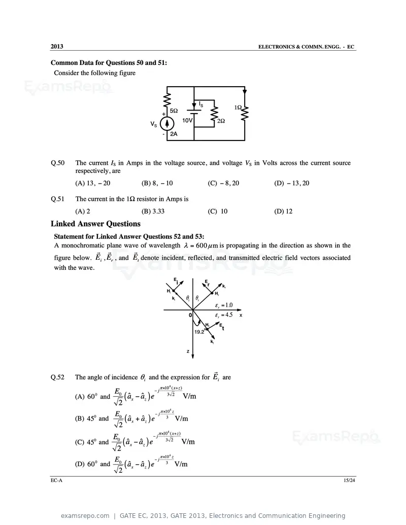
Text of page 16
2013                                                                                                          ELECTRONICS & COMMN. ENGG. - EC


Common Data for Questions 50 and 51:
 Consider the following figure


                                                                        IS
                                                                                                         1Ω
                                              + 5Ω
                                       VS
                                                                 10V                        2Ω

                                               - 2A


Q.50    The current IS in Amps in the voltage source, and voltage VS in Volts across the current source
        respectively, are
        (A) 13, − 20                (B) 8, − 10                                   (C) − 8, 20                      (D) − 13, 20

Q.51    The current in the 1Ω resistor in Amps is
        (A) 2                       (B) 3.33                                      (C) 10                           (D) 12
Linked Answer Questions
 Statement for Linked Answer Questions 52 and 53:
 A monochromatic plane wave of wavelength λ = 600 µ m is propagating in the direction as shown in the
                    r   r       r
 figure below. Ei , Er , and Et denote incident, reflected, and transmitted electric field vectors associated
 with the wave.
                                                         E
                                                             i                E
                                                                                  r                 kr
                                                  Hi
                                                                                           Hr
                                                        ki        θi θ r
                                                                                           ε r = 1.0
                                                                   0                       ε r = 4.5      x
                                                                              Ht                E
                                                                              0                 t
                                                                       19.2
                                                                                      kt

                                                                  z


                                                                                           r
Q.52    The angle of incidence θ i and the expression for Ei are
                                             π ×104 ( x + z )
                    E                   −j
        (A) 60 and 0 ( aˆ x − aˆ z ) e
                0                              3 2
                                                   V/m
                     2
                                           π ×10 z  4
                    E0                  −j
        (B) 450 and    ( aˆ x + aˆ z ) e 3 V/m
                     2
                                            π ×104 ( x + z )
                    E                   −j
        (C) 45 and 0 ( aˆ x − aˆ z ) e
                0                              3 2
                                                      V/m
                     2
                                            π ×10 z4
                    E                    −j
        (D) 60 0 and 0 ( aˆ x − aˆ z ) e       3
                                                    V/m
                      2
EC-A                                                                                                                                     15/24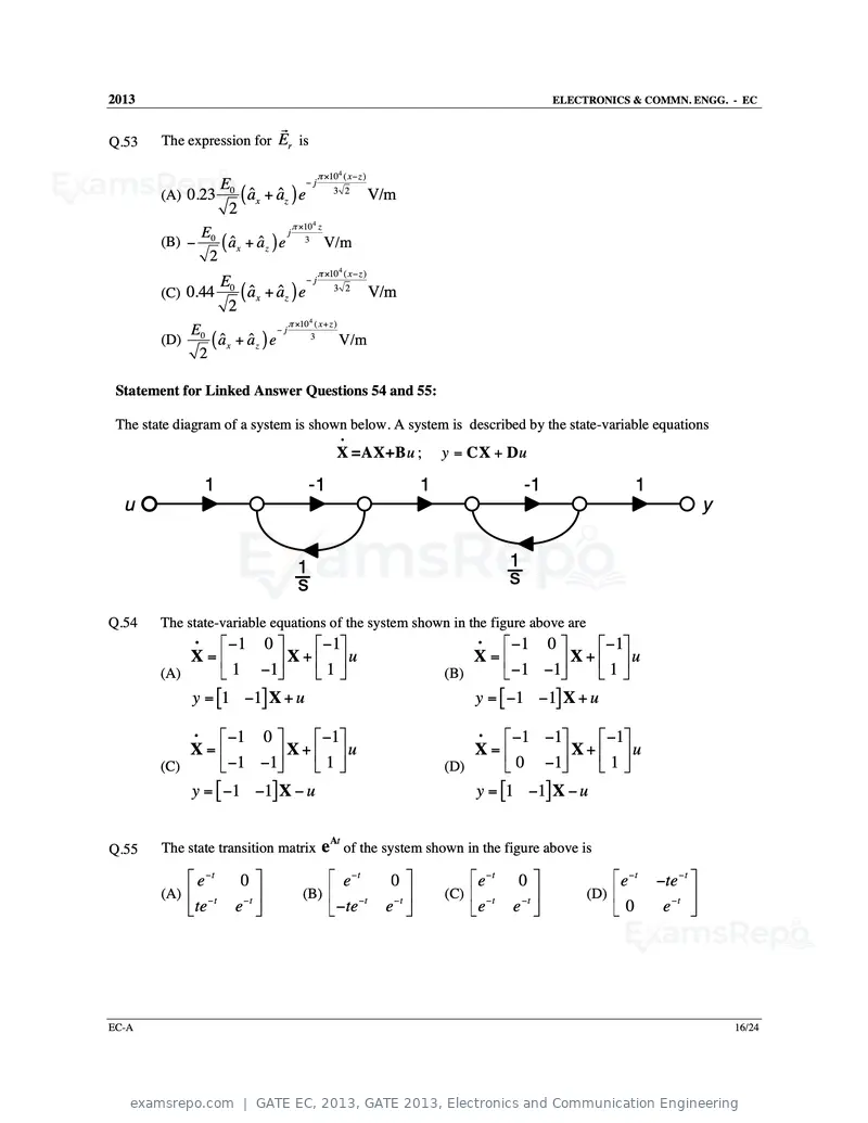
Text of page 17
2013 ELECTRONICS & COMMN. ENGG. - EC
r
Q.53 The expression for Er is
π ×104 ( x − z )
E −j
(A) 0.23 0 ( aˆ x + aˆ z ) e 3 2
V/m
2
π ×10 z 4
E
(B) − 0 ( aˆ x + aˆ z ) e 3 V/m
j
2
π ×104 ( x − z )
E −j
(C) 0.44 0 ( aˆ x + aˆ z ) e 3 2
V/m
2
π ×10 ( x + z )
4
E −j
(D) 0 ( aˆ x + aˆ z ) e 3
V/m
2
Statement for Linked Answer Questions 54 and 55:
The state diagram of a system is shown below. A system is described by the state-variable equations
•
X =AX+B u ; y = CX + D u
1 -1 1 -1 1
u y
1 1
s s
Q.54 The state-variable equations of the system shown in the figure above are
• −1 0 −1 • −1 0 −1
X= X+ u X= X+ u
(A) 1 −1 1 (B) −1 −1 1
y = [1 −1] X + u y = [ −1 −1] X + u
• −1 0 −1 • −1 −1 −1
X= X+ u X= X+ u
(C) −1 −1 1 (D) 0 −1 1
y = [ −1 −1] X − u y = [1 −1] X − u
At
Q.55 The state transition matrix e of the system shown in the figure above is
e −t 0 e−t 0 e−t 0 e −t −te − t
(A) − t (B) (C) − t (D)
te e −t −te
−t
e−t e e −t 0 e−t
EC-A 16/24
Text of page 18
2013                                                                       ELECTRONICS & COMMN. ENGG. - EC


General Aptitude (GA) Questions

Q.56 to Q.60 carry one mark each.
 Q.56   Choose the grammatically CORRECT sentence:
        (A) Two and two add four.
        (B) Two and two become four.
        (C) Two and two are four.
        (D) Two and two make four.

 Q.57   Statement: You can always give me a ring whenever you need.
        Which one of the following is the best inference from the above statement?
        (A) Because I have a nice caller tune.
        (B) Because I have a better telephone facility.
        (C) Because a friend in need is a friend indeed.
        (D) Because you need not pay towards the telephone bills when you give me a ring.

 Q.58   In the summer of 2012, in New Delhi, the mean temperature of Monday to Wednesday was 41°C
        and of Tuesday to Thursday was 43°C. If the temperature on Thursday was 15% higher than that of
        Monday, then the temperature in °C on Thursday was
        (A) 40                   (B) 43                  (C) 46                  (D) 49

 Q.59   Complete the sentence:
        Dare _______________ mistakes.
        (A) commit               (B) to commit           (C) committed           (D) committing

 Q.60   They were requested not to quarrel with others.
        Which one of the following options is the closest in meaning to the word quarrel?
        (A) make out             (B) call out            (C) dig out             (D) fall out

Q.61 to Q.65 carry two marks each.
 Q.61   A car travels 8 km in the first quarter of an hour, 6 km in the second quarter and 16 km in the third
        quarter. The average speed of the car in km per hour over the entire journey is
        (A) 30                   (B) 36                  (C) 40                  (D) 24

 Q.62   Find the sum to n terms of the series 10+84+ 734 + .....

        (A)
              (
            9 9n + 1 )
                     +1
               10
        (B)
              (
            9 9n − 1 )
                     +1
               8
        (C)
              (
            9 9n −1  )
                     +n
               8
        (D)
              (
            9 9n − 1 )
                     + n2
                8
EC-A                                                                                                      17/24
Text of page 19
2013                                                                       ELECTRONICS & COMMN. ENGG. - EC


 Q.63   Statement: There were different streams of freedom movements in colonial India carried out by the
        moderates, liberals, radicals, socialists, and so on.
        Which one of the following is the best inference from the above statement?
        (A) The emergence of nationalism in colonial India led to our Independence.
        (B) Nationalism in India emerged in the context of colonialism.
        (C) Nationalism in India is homogeneous.
        (D) Nationalism in India is heterogeneous.

 Q.64   The set of values of p for which the roots of the equation 3x2+2x+p(p–1) = 0 are of opposite sign is
        (A) (–∞, 0)             (B) (0, 1)              (C) (1, ∞)              (D) (0, ∞)

 Q.65   What is the chance that a leap year, selected at random, will contain 53 Saturdays?
        (A) 2/7                 (B) 3/7                 (C) 1/7                 (D) 5/7


                              END OF THE QUESTION PAPER


EC-A                                                                                                      18/24
Text of page 20
SESSION - 2
Text of page 21
2013                                                                      Question Booklet Code
                                                                                                         B
         `EC : ELECTRONICS AND COMMUNICATION ENGINEERING
Duration: Three Hours                                                                     Maximum Marks: 100

Read the following instructions carefully.

    1. Do not open the seal of the Question Booklet until you are asked to do so by the invigilator.
    2. Take out the Optical Response Sheet (ORS) from this Question Booklet without breaking the seal
        and read the instructions printed on the ORS carefully. If you find that either:
        a. The Question Booklet Code printed at the right hand top corner of this page does not match with
             the Question Booklet Code at the right hand top corner of the ORS or
        b. The Question Paper Code preceding the Registration number on the ORS is not EC,
       then exchange the booklet immediately with a new sealed Question Booklet.
    3. On the right hand side of the ORS, using ONLY a black ink ballpoint pen, (i) darken the appropriate
       bubble under each digit of your registration number and (ii) write your registration number, your
       name and name of the examination centre and put your signature at the specified location.
    4. This Question Booklet contains 24 pages including blank pages for rough work. After you are
       permitted to open the seal, check all pages and report discrepancies, if any, to the invigilator.
    5. There are a total of 65 questions carrying 100 marks. All these questions are of objective type. Each
       question has only one correct answer. Questions must be answered on the left hand side of the ORS
       by darkening the appropriate bubble (marked A, B, C, D) using ONLY a black ink ballpoint pen
       against the question number. For each question darken the bubble of the correct answer. More
       than one answer bubbled against a question will be treated as an incorrect response.
    6. Since bubbles darkened by the black ink ballpoint pen cannot be erased, candidates should darken the
       bubbles in the ORS very carefully.
    7. Questions Q.1 – Q.25 carry 1 mark each. Questions Q.26 – Q.55 carry 2 marks each. The 2 marks
       questions include two pairs of common data questions and two pairs of linked answer questions. The
       answer to the second question of the linked answer questions depends on the answer to the first
       question of the pair. If the first question in the linked pair is wrongly answered or is not attempted,
       then the answer to the second question in the pair will not be evaluated.
    8. Questions Q.56 – Q.65 belong to General Aptitude (GA) section and carry a total of 15 marks.
       Questions Q.56 – Q.60 carry 1 mark each, and questions Q.61 – Q.65 carry 2 marks each.
    9. Questions not attempted will result in zero mark and wrong answers will result in NEGATIVE
       marks. For all 1 mark questions, ⅓ mark will be deducted for each wrong answer. For all 2 marks
       questions, ⅔ mark will be deducted for each wrong answer. However, in the case of the linked
       answer question pair, there will be negative marks only for wrong answer to the first question and no
       negative marks for wrong answer to the second question.
    10. Calculator is allowed whereas charts, graph sheets or tables are NOT allowed in the examination hall.
    11. Rough work can be done on the Question Booklet itself. Blank pages are provided at the end of the
        Question Booklet for rough work.
    12. Before the start of the examination, write your name and registration number in the space provided
        below using a black ink ballpoint pen.

           Name

           Registration Number         EC
EC-B                                                                                                      1/24
Text of page 22
2013                                                                              ELECTRONICS & COMMN. ENGG. - EC


Q.1 to Q.25 carry one mark each.


Q.1    For a periodic signal v (t ) = 30 sin 100 t + 10 cos 300 t + 6 sin (500 t + π / 4) , the fundamental frequency in
       rad/s is
       (A) 100                    (B) 300                    (C) 500                    (D) 1500


Q.2    In a voltage-voltage feedback as shown below, which one of the following statements is TRUE if
       the gain k is increased?


       (A) The input impedance increases and output impedance decreases.
       (B) The input impedance increases and output impedance also increases.
       (C) The input impedance decreases and output impedance also decreases.
       (D) The input impedance decreases and output impedance increases.

Q.3    A band-limited signal with a maximum frequency of 5 kHz is to be sampled. According to the
       sampling theorem, the sampling frequency which is not valid is
       (A) 5 kHz                  (B) 12 kHz                 (C) 15 kHz                 (D) 20 kHz

Q.4    In a MOSFET operating in the saturation region, the channel length modulation effect causes
       (A)   an increase in the gate-source capacitance
       (B)   a decrease in the transconductance
       (C)   a decrease in the unity-gain cutoff frequency
       (D)   a decrease in the output resistance

Q.5    Which one of the following statements is NOT TRUE for a continuous time causal and stable
       LTI system?
       (A) All the poles of the system must lie on the left side of the jω axis.
       (B) Zeros of the system can lie anywhere in the s-plane.
       (C) All the poles must lie within s = 1 .
       (D) All the roots of the characteristic equation must be located on the left side of the jω axis.


EC-B                                                                                                                  2/24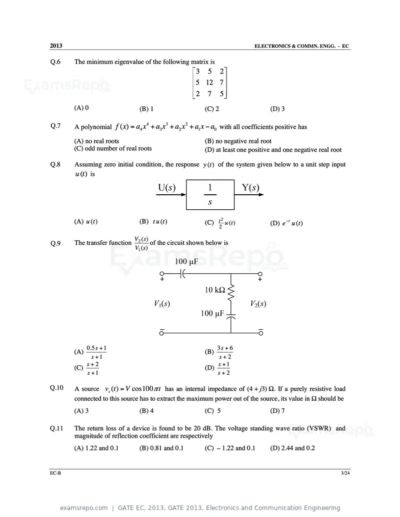
Text of page 23
2013 ELECTRONICS & COMMN. ENGG. - EC
Q.6 The minimum eigenvalue of the following matrix is
3 5 2
5 12 7
2 7 5
(A) 0 (B) 1 (C) 2 (D) 3
A polynomial f ( x) = a4 x + a3 x + a2 x + a1 x − a0 with all coefficients positive has
4 3 2
Q.7
(A) no real roots (B) no negative real root
(C) odd number of real roots (D) at least one positive and one negative real root
Q.8 Assuming zero initial condition, the response y (t ) of the system given below to a unit step input
u (t ) is
2
(A) u (t ) (B) t u (t ) (C) t u (t )
2
(D) e − t u (t )
V2 ( s )
Q.9 The transfer function of the circuit shown below is
V1 ( s )
0.5 s + 1 3s + 6
(A) (B)
s +1 s+2
s+2 s +1
(C) (D)
s +1 s+2
Q.10 A source vs (t ) = V cos100 π t has an internal impedance of (4 + j3) Ω. If a purely resistive load
connected to this source has to extract the maximum power out of the source, its value in Ω should be
(A) 3 (B) 4 (C) 5 (D) 7
Q.11 The return loss of a device is found to be 20 dB. The voltage standing wave ratio (VSWR) and
magnitude of reflection coefficient are respectively
(A) 1.22 and 0.1 (B) 0.81 and 0.1 (C) − 1.22 and 0.1 (D) 2.44 and 0.2
EC-B 3/24
Text of page 24
2013                                                                                ELECTRONICS & COMMN. ENGG. - EC


                        − π t2
Q.12   Let g (t ) = e    , and h ( t ) is a filter matched to g ( t ) . If g ( t ) is applied as input to h ( t ) , then
       the Fourier transform of the output is
                                               2                                                      2

       (A) e −π f                    (B) e−π f /2            (C) e −π | f |              (D) e−2π f
                    2


                               r r                                              r   r
Q.13   Consider a vector field A( r ) . The closed loop line integral         ∫ A • dl can be expressed as
                        r        r
       (A) ∫∫ (∇× A)r• ds over the closed surface bounded by the loop
       (B) ∫∫∫ (∇ • A)dv over the closed volume bounded by the loop
                     r
       (C) ∫∫∫ (∇ • A)dv over the open volume bounded by the loop
                   r     r
       (D) ∫∫ (∇ × A) • ds over the open surface bounded by the loop


Q.14   A bulb in a staircase has two switches, one switch being at the ground floor and the other one at the
       first floor. The bulb can be turned ON and also can be turned OFF by any one of the switches
       irrespective of the state of the other switch. The logic of switching of the bulb resembles
       (A) an AND gate               (B) an OR gate          (C) an XOR gate             (D) a NAND gate

Q.15   Two systems with impulse responses h1 (t ) and h2 (t ) are connected in cascade. Then the overall
       impulse response of the cascaded system is given by
       (A) product of h1 (t ) and h2 (t )
       (B) sum of h1 (t ) and h2 (t )
       (C) convolution of h1 (t ) and h2 (t )
       (D) subtraction of h2 (t ) from h1 (t )

Q.16   In a forward biased pn junction diode, the sequence of events that best describes the mechanism of
       current flow is
       (A)   injection, and subsequent diffusion and recombination of minority carriers
       (B)   injection, and subsequent drift and generation of minority carriers
       (C)   extraction, and subsequent diffusion and generation of minority carriers
       (D)   extraction, and subsequent drift and recombination of minority carriers

Q.17   In IC technology, dry oxidation (using dry oxygen) as compared to wet oxidation (using steam or
       water vapor) produces
       (A)   superior quality oxide with a higher growth rate
       (B)   inferior quality oxide with a higher growth rate
       (C)   inferior quality oxide with a lower growth rate
       (D)   superior quality oxide with a lower growth rate

Q.18   The maximum value of θ until which the approximation sin θ ≈ θ holds to within 10% error is
       (A) 10°                       (B) 18°                 (C) 50°                     (D) 90°

EC-B                                                                                                                  4/24
Text of page 25
2013                                                                                            ELECTRONICS & COMMN. ENGG. - EC

                                                          r
Q.19   The divergence of the vector field A = xaˆ x + yaˆ y + zaˆ z is

       (A) 0                            (B) 1/3                     (C) 1                            (D) 3

Q.20   The impulse response of a system is h(t ) = t u (t ) . For an input u (t − 1) , the output is

             t2                               t (t −1)                    (t −1) 2                         t 2 −1
       (A)        u (t )                (B)              u (t −1)   (C)              u (t −1)        (D)            u (t −1)
             2                                  2                           2                                2


Q.21   The Bode plot of a transfer function G (s ) is shown in the figure below.


                            Gain (dB)


       The gain (20 log G ( s) ) is 32 dB and −8 dB at 1 rad/s and 10 rad/s respectively. The phase is
       negative for all ω. Then G (s) is

             39.8                             39.8                        32                                 32
       (A)                              (B)                         (C)                              (D)
              s                                s2                          s                                 s2

Q.22   In the circuit shown below what is the output voltage (Vout) if a silicon transistor Q and an ideal
       op-amp are used?


                                                                     +15 V                            Q
                                                    1 kΩ
                                                                    –
                                                                    +                                  Vout
                            5V
                                                                     – 15 V


       (A)       15 V                   (B)     0.7 V               (C)     0.7 V                    (D)      15 V


EC-B                                                                                                                           5/24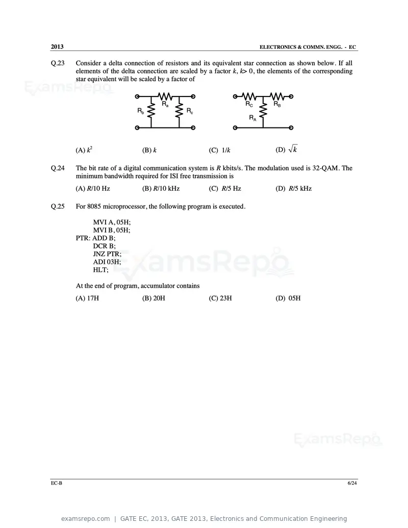
Text of page 26
2013                                                                       ELECTRONICS & COMMN. ENGG. - EC


Q.23   Consider a delta connection of resistors and its equivalent star connection as shown below. If all
       elements of the delta connection are scaled by a factor k, k> 0, the elements of the corresponding
       star equivalent will be scaled by a factor of


                                      Ra                             RC        RB
                            Rb                Rc
                                                                      RA


       (A) k2                 (B) k                   (C) 1/k                   (D)   k

Q.24   The bit rate of a digital communication system is R kbits/s. The modulation used is 32-QAM. The
       minimum bandwidth required for ISI free transmission is
       (A) R/10 Hz            (B) R/10 kHz            (C) R/5 Hz                (D) R/5 kHz

Q.25   For 8085 microprocessor, the following program is executed.

            MVI A, 05H;
            MVI B, 05H;
       PTR: ADD B;
            DCR B;
            JNZ PTR;
            ADI 03H;
            HLT;

       At the end of program, accumulator contains
       (A) 17H                (B) 20H                 (C) 23H                   (D) 05H


EC-B                                                                                                   6/24
Text of page 27
2013 ELECTRONICS & COMMN. ENGG. - EC
Q.26 to Q.55 carry two marks each.
Q.26 Consider two identically distributed zero-mean random variables U and V . Let the cumulative
distribution functions of U and 2V be F ( x ) and G ( x ) respectively. Then, for all values of x
(A) F ( x ) − G ( x ) ≤ 0 (B) F ( x ) − G ( x ) ≥ 0
(C) ( F ( x ) − G ( x )) ⋅ x ≤ 0 (D) ( F ( x ) − G ( x )) ⋅ x ≥ 0
Q.27 A system described by a linear, constant coefficient, ordinary, first order differential equation has
an exact solution given by y (t ) for t > 0 , when the forcing function is x(t ) and the initial
condition is y (0) . If one wishes to modify the system so that the solution becomes
−2 y(t ) for t > 0 , we need to
(A) change the initial condition to − y(0) and the forcing function to 2 x(t )
(B) change the initial condition to 2 y (0) and the forcing function to − x(t )
(C) change the initial condition to j 2 y (0) and the forcing function to j 2 x (t )
(D) change the initial condition to −2 y (0) and the forcing function to −2 x (t )
Q.28 The DFT of a vector [ a b c d ] is the vector [α β γ δ ] . Consider the product
a b c d
d a b c
[p q r s] = [a b c d ]
c
.
d a b
b c d a
The DFT of the vector [ p q r s ] is a scaled version of
(A) α β 2 γ 2 δ 2 (B) α β γ δ
2
(C) [α + β β + δ δ + γ γ + α ] (D) [α β γ δ]
Y (s)
Q.29 The signal flow graph for a system is given below. The transfer function for this system is
U ( s)
1
U(s) 1 s-1 s-1 1 Y(s)
–4
–2
s +1 s +1
(A) (B)
5s2 + 6s + 2 s2 + 6 s + 2
s +1 1
(C) (D)
s2 + 4 s + 2 5s2 + 6s + 2
EC-B 7/24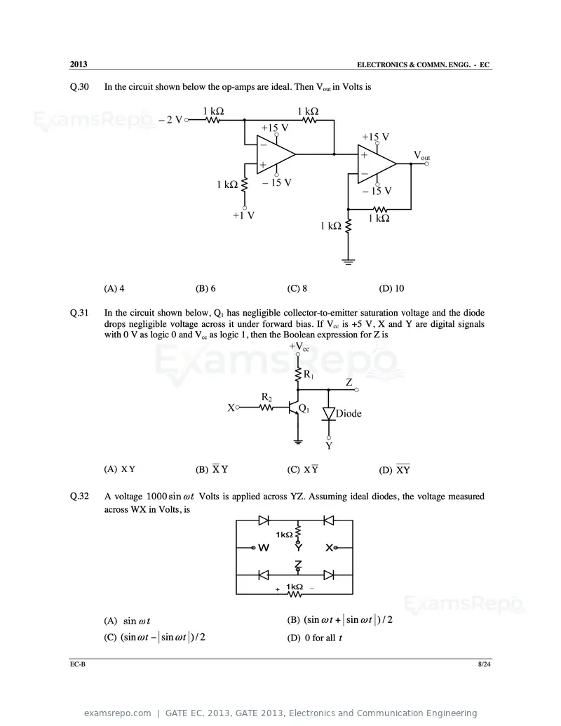
Text of page 28
2013                                                                      ELECTRONICS & COMMN. ENGG. - EC


Q.30   In the circuit shown below the op-amps are ideal. Then Vout in Volts is


       (A) 4                    (B) 6                   (C) 8                    (D) 10

Q.31   In the circuit shown below, Q1 has negligible collector-to-emitter saturation voltage and the diode
       drops negligible voltage across it under forward bias. If Vcc is +5 V, X and Y are digital signals
       with 0 V as logic 0 and Vcc as logic 1, then the Boolean expression for Z is


       (A) X Y                  (B) X Y                 (C) X Y                  (D) XY

Q.32   A voltage 1000 sin ω t Volts is applied across YZ. Assuming ideal diodes, the voltage measured
       across WX in Volts, is

                                                    1kΩ
                                               W          Y         X
                                                          Z

                                                    +   1kΩ     _


       (A) sin ω t                                      (B) (sin ω t + sin ω t ) / 2
       (C) (sin ω t − sin ω t ) / 2                     (D) 0 for all t

EC-B                                                                                                    8/24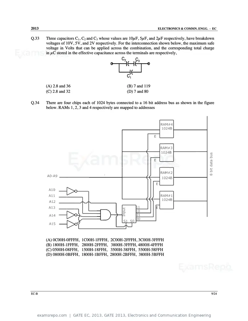
Text of page 29
2013                                                                   ELECTRONICS & COMMN. ENGG. - EC


Q.33   Three capacitors C1, C2 and C3 whose values are 10µF, 5µF, and 2µF respectively, have breakdown
       voltages of 10V, 5V, and 2V respectively. For the interconnection shown below, the maximum safe
       voltage in Volts that can be applied across the combination, and the corresponding total charge
       in µC stored in the effective capacitance across the terminals are respectively,
                                                  C2        C3


                                                       C1

       (A) 2.8 and 36                                  (B) 7 and 119
       (C) 2.8 and 32                                  (D) 7 and 80

Q.34   There are four chips each of 1024 bytes connected to a 16 bit address bus as shown in the figure
       below. RAMs 1, 2, 3 and 4 respectively are mapped to addresses


       (A) 0C00H-0FFFH, 1C00H-1FFFH, 2C00H-2FFFH, 3C00H-3FFFH
       (B) 1800H-1FFFH, 2800H-2FFFH, 3800H-3FFFH, 4800H-4FFFH
       (C) 0500H-08FFH, 1500H-18FFH, 3500H-38FFH, 5500H-58FFH
       (D) 0800H-0BFFH, 1800H-1BFFH, 2800H-2BFFH, 3800H-3BFFH


EC-B                                                                                                 9/24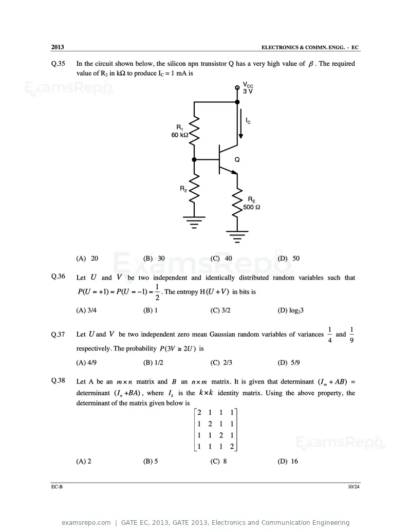
Text of page 30
2013 ELECTRONICS & COMMN. ENGG. - EC
Q.35 In the circuit shown below, the silicon npn transistor Q has a very high value of β . The required
value of R2 in kΩ to produce IC = 1 mA is
VCC
3V
IC
R1
60 kΩ
Q
R2
RE
500 Ω
(A) 20 (B) 30 (C) 40 (D) 50
Q.36 Let U and V be two independent and identically distributed random variables such that
1
P(U = +1) = P(U = −1) = . The entropy H (U + V ) in bits is
2
(A) 3/4 (B) 1 (C) 3/2 (D) log23
1 1
Q.37 Let U and V be two independent zero mean Gaussian random variables of variances and
4 9
respectively. The probability P (3V ≥ 2U ) is
(A) 4/9 (B) 1/2 (C) 2/3 (D) 5/9
Q.38 Let A be an m × n matrix and B an n × m matrix. It is given that determinant ( I m + AB ) =
determinant ( I n +BA) , where I k is the k × k identity matrix. Using the above property, the
determinant of the matrix given below is
2 1 1 1
1 2 1 1
1 1 2 1
1 1 1 2
(A) 2 (B) 5 (C) 8 (D) 16
EC-B 10/24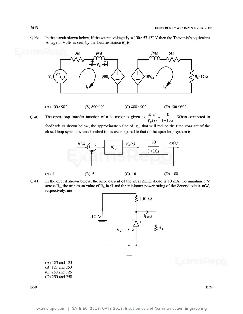
Text of page 31
2013                                                                      ELECTRONICS & COMMN. ENGG. - EC


Q.39   In the circuit shown below, if the source voltage VS = 100∠53.13° V then the Thevenin’s equivalent
       voltage in Volts as seen by the load resistance RL is

                         3Ω           j4 Ω                            j6 Ω            5Ω


                                      VL1


        VS                                  j40I2                 10VL1                        RL=10 Ω

                               I1                                                I2


       (A) 100∠90°            (B) 800∠0°              (C) 800∠90°                (D) 100∠60°
                                                                    ω (s)     10
Q.40   The open-loop transfer function of a dc motor is given as             =      . When connected in
                                                                   Va ( s) 1 + 10 s
       feedback as shown below, the approximate value of K a that will reduce the time constant of the
       closed loop system by one hundred times as compared to that of the open-loop system is


       (A) 1                  (B) 5                   (C) 10                     (D) 100
Q.41   In the circuit shown below, the knee current of the ideal Zener diode is 10 mA. To maintain 5 V
       across RL, the minimum value of RL in Ω and the minimum power rating of the Zener diode in mW,
       respectively, are


       (A) 125 and 125
       (B) 125 and 250
       (C) 250 and 125
       (D) 250 and 250

EC-B                                                                                                  11/24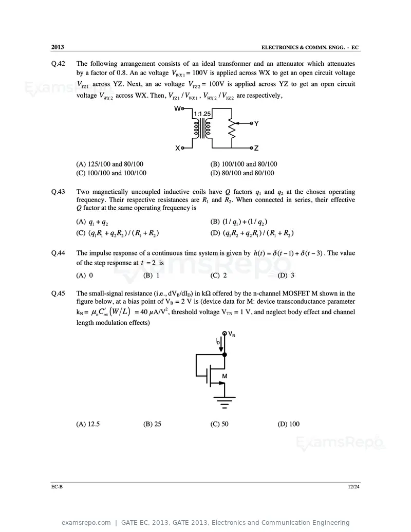
Text of page 32
2013                                                                           ELECTRONICS & COMMN. ENGG. - EC


Q.42   The following arrangement consists of an ideal transformer and an attenuator which attenuates
       by a factor of 0.8. An ac voltage VWX 1 = 100V is applied across WX to get an open circuit voltage
       VYZ 1 across YZ. Next, an ac voltage VYZ 2 = 100V is applied across YZ to get an open circuit
       voltage VWX 2 across WX. Then, VYZ 1 / VWX 1 , VWX 2 / VYZ 2 are respectively,
                                             W
                                                   1:1.25
                                                                           Y


                                             X                             Z

       (A) 125/100 and 80/100                            (B) 100/100 and 80/100
       (C) 100/100 and 100/100                           (D) 80/100 and 80/100

Q.43   Two magnetically uncoupled inductive coils have Q factors q1 and q2 at the chosen operating
       frequency. Their respective resistances are R1 and R2. When connected in series, their effective
       Q factor at the same operating frequency is
       (A) q1 + q2                                       (B) (1/ q1 ) + (1/ q2 )
       (C) ( q1 R1 + q2 R2 ) / ( R1 + R2 )               (D) ( q1 R2 + q2 R1 ) / ( R1 + R2 )

Q.44   The impulse response of a continuous time system is given by h (t ) = δ (t − 1) + δ (t − 3) . The value
       of the step response at t = 2 is
       (A) 0                       (B) 1                 (C) 2                       (D) 3

Q.45   The small-signal resistance (i.e., dVB/dID) in kΩ offered by the n-channel MOSFET M shown in the
       figure below, at a bias point of VB = 2 V is (device data for M: device transconductance parameter
                 ′ (W L ) = 40 µA/V2, threshold voltage VTN = 1 V, and neglect body effect and channel
       kN = µn Cox
       length modulation effects)
                                                                     VB
                                                            ID


                                                                 M


       (A) 12.5                    (B) 25                (C) 50                      (D) 100


EC-B                                                                                                       12/24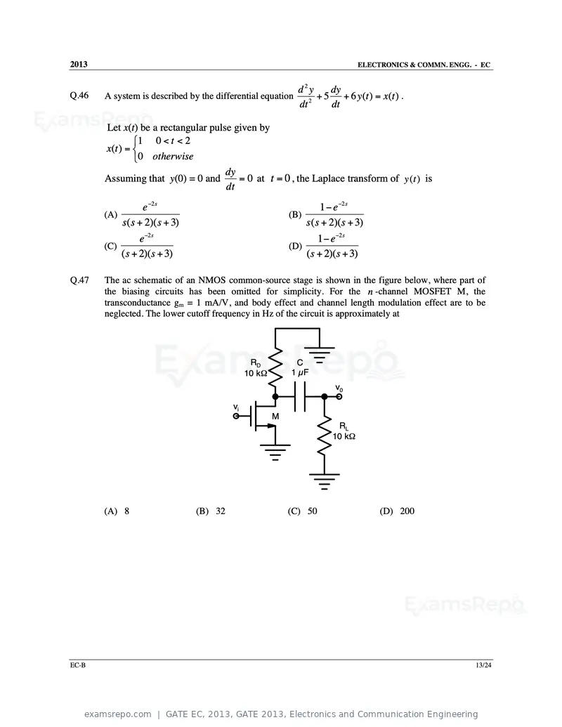
Text of page 33
2013 ELECTRONICS & COMMN. ENGG. - EC
d2y dy
Q.46 A system is described by the differential equation 2
+ 5 + 6 y (t ) = x(t ) .
dt dt
Let x(t) be a rectangular pulse given by
1 0 < t < 2
x (t ) =
0 otherwise
dy
Assuming that y(0) = 0 and = 0 at t = 0 , the Laplace transform of y ( t ) is
dt
e−2 s 1 − e−2 s
(A) (B)
s ( s + 2)( s + 3) s ( s + 2)( s + 3)
e−2s 1 − e−2 s
(C) (D)
(s + 2)(s + 3) (s + 2)(s + 3)
Q.47 The ac schematic of an NMOS common-source stage is shown in the figure below, where part of
the biasing circuits has been omitted for simplicity. For the n -channel MOSFET M, the
transconductance gm = 1 mA/V, and body effect and channel length modulation effect are to be
neglected. The lower cutoff frequency in Hz of the circuit is approximately at
RD C
10 kΩ 1 µF
v0
vi
M
RL
10 kΩ
(A) 8 (B) 32 (C) 50 (D) 200
EC-B 13/24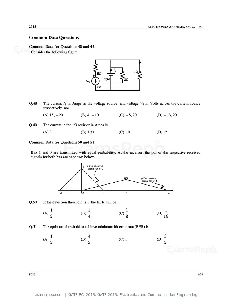
Text of page 34
2013                                                                                        ELECTRONICS & COMMN. ENGG. - EC


Common Data Questions
Common Data for Questions 48 and 49:
 Consider the following figure


                                                                IS
                                                                                 1Ω
                                           + 5Ω
                                     VS
                                                          10V              2Ω

                                            - 2A


Q.48    The current IS in Amps in the voltage source, and voltage VS in Volts across the current source
        respectively, are
        (A) 13, − 20            (B) 8, − 10                          (C) − 8, 20                      (D) − 13, 20

Q.49    The current in the 1Ω resistor in Amps is
        (A) 2                   (B) 3.33                             (C) 10                           (D) 12

Common Data for Questions 50 and 51:

 Bits 1 and 0 are transmitted with equal probability. At the receiver, the pdf of the respective received
 signals for both bits are as shown below.

                                      pdf of received
                                 1
                                       signal for bit 0


                                                                           0.5        pdf of received
                                                                                       signal for bit 1


                  -1             0                        1                2                                     4


Q.50    If the detection threshold is 1, the BER will be

              1                       1                                     1                                1
        (A)                     (B)                                  (C)                              (D)
              2                       4                                     8                               16

Q.51    The optimum threshold to achieve minimum bit error rate (BER) is

              1                       4                                                                     3
        (A)                     (B)                                  (C) 1                            (D)
              2                       5                                                                     2


EC-B                                                                                                                   14/24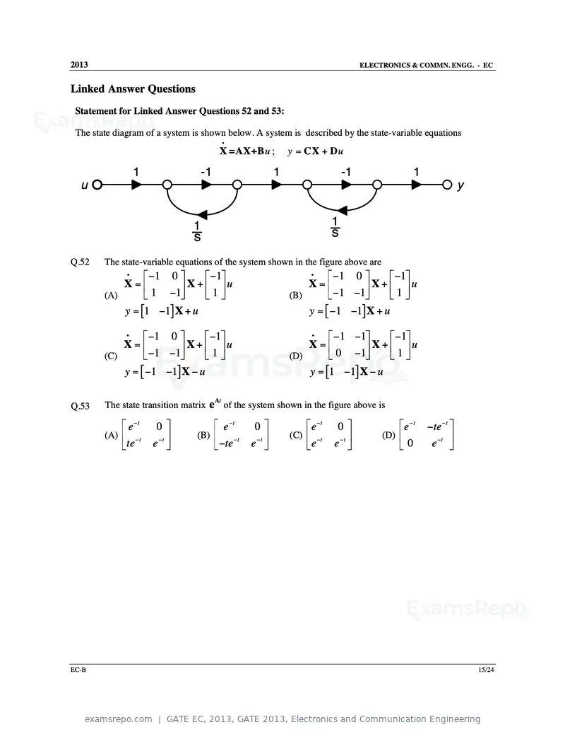
Text of page 35
2013 ELECTRONICS & COMMN. ENGG. - EC
Linked Answer Questions
Statement for Linked Answer Questions 52 and 53:
The state diagram of a system is shown below. A system is described by the state-variable equations
•
X =AX+B u ; y = CX + D u
1 -1 1 -1 1
u y
1 1
s s
Q.52 The state-variable equations of the system shown in the figure above are
• −1 0 −1 • −1 0 −1
X= X+ u X= X+ u
(A) 1 −1 1 (B) −1 −1 1
y = [1 −1] X + u y = [ −1 −1] X + u
• −1 0 −1 • −1 −1 −1
X= X + 1 u X= X + 1 u
(C) −1 −1 (D) 0 −1
y = [ −1 −1] X − u y = [1 −1] X − u
At
Q.53 The state transition matrix e of the system shown in the figure above is
e −t 0 e−t 0 e−t 0 e −t −te − t
(A) − t (B) (C) − t (D)
te e −t −te
−t
e−t e e −t 0 e−t
EC-B 15/24
Text of page 36
2013                                                                                                                ELECTRONICS & COMMN. ENGG. - EC


 Statement for Linked Answer Questions 54 and 55:
 A monochromatic plane wave of wavelength λ = 600 µ m is propagating in the direction as shown in the
                 r    r           r
 figure below. Ei , Er , and Et denote incident, reflected, and transmitted electric field vectors associated
 with the wave.
                                                                   E
                                                                    i                E
                                                                                         r                 kr
                                                          Hi
                                                                                                  Hr
                                                               ki        θi θ r
                                                                                                  ε r = 1.0
                                                                          0                       ε r = 4.5     x
                                                                                     Ht                E
                                                                                     0                     t
                                                                              19.2
                                                                                             kt

                                                                         z


                                                                                                  r
Q.54    The angle of incidence θ i and the expression for Ei are
                                                      π ×104 ( x + z )
                     E                   −j
        (A) 60 0 and 0 ( aˆ x − aˆ z ) e        3 2
                                                    V/m
                      2
                                            π ×10 z            4
                     E0                  −j
        (B) 450 and     ( aˆ x + aˆ z ) e 3 V/m
                      2
                                                     π ×104 ( x + z )
                    E                   −j
        (C) 450 and 0 ( aˆ x − aˆ z ) e        3 2
                                                      V/m
                     2
                                            π ×10 z            4
                    E                    −j
        (D) 60 0 and 0 ( aˆ x − aˆ z ) e       3
                                                    V/m
                      2
                                 r
Q.55    The expression for Er is

                                               π ×104 ( x − z )
                 E                     −j
        (A) 0.23 0 ( aˆ x + aˆ z ) e       3 2
                                               V/m
                  2
                                   π ×10 z 4
              E
        (B) − 0 ( aˆ x + aˆ z ) e 3 V/m
                                 j

               2
                                               π ×104 ( x − z )
                 E                     −j
        (C) 0.44 0 ( aˆ x + aˆ z ) e             3 2
                                                       V/m
                    2
                                   π ×10 ( x + z )
                                       4
             E                  −j
        (D) 0 ( aˆ x + aˆ z ) e         3
                                                   V/m
              2


EC-B                                                                                                                                           16/24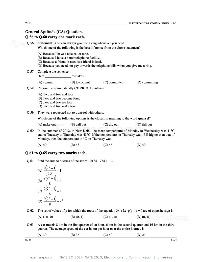
Text of page 37
2013                                                                       ELECTRONICS & COMMN. ENGG. - EC


General Aptitude (GA) Questions
Q.56 to Q.60 carry one mark each.
 Q.56   Statement: You can always give me a ring whenever you need.
        Which one of the following is the best inference from the above statement?
        (A) Because I have a nice caller tune.
        (B) Because I have a better telephone facility.
        (C) Because a friend in need is a friend indeed.
        (D) Because you need not pay towards the telephone bills when you give me a ring.
 Q.57   Complete the sentence:
        Dare _______________ mistakes.
        (A) commit              (B) to commit            (C) committed           (D) committing
 Q.58   Choose the grammatically CORRECT sentence:
        (A) Two and two add four.
        (B) Two and two become four.
        (C) Two and two are four.
        (D) Two and two make four.
 Q.59   They were requested not to quarrel with others.
        Which one of the following options is the closest in meaning to the word quarrel?
        (A) make out            (B) call out             (C) dig out             (D) fall out
 Q.60   In the summer of 2012, in New Delhi, the mean temperature of Monday to Wednesday was 41°C
        and of Tuesday to Thursday was 43°C. If the temperature on Thursday was 15% higher than that of
        Monday, then the temperature in °C on Thursday was
        (A) 40                  (B) 43                   (C) 46                  (D) 49

Q.61 to Q.65 carry two marks each.
 Q.61   Find the sum to n terms of the series 10+84+ 734 + .....

        (A)
              (
            9 9n + 1  )
                     +1
               10
        (B)
              (
            9 9n − 1  )
                     +1
               8
        (C)
              (
            9 9n −1   )
                     +n
               8
        (D)
              (
            9 9n − 1  )
                     + n2
                8
 Q.62   The set of values of p for which the roots of the equation 3x2+2x+p(p–1) = 0 are of opposite sign is
        (A) (–∞, 0)             (B) (0, 1)               (C) (1, ∞)              (D) (0, ∞)

 Q.63   A car travels 8 km in the first quarter of an hour, 6 km in the second quarter and 16 km in the third
        quarter. The average speed of the car in km per hour over the entire journey is
        (A) 30                  (B) 36                   (C) 40                  (D) 24
EC-B                                                                                                      17/24
Text of page 38
2013                                                                      ELECTRONICS & COMMN. ENGG. - EC


 Q.64   What is the chance that a leap year, selected at random, will contain 53 Saturdays?
        (A) 2/7                 (B) 3/7                 (C) 1/7                 (D) 5/7

 Q.65   Statement: There were different streams of freedom movements in colonial India carried out by the
        moderates, liberals, radicals, socialists, and so on.
        Which one of the following is the best inference from the above statement?
        (A) The emergence of nationalism in colonial India led to our Independence.
        (B) Nationalism in India emerged in the context of colonialism.
        (C) Nationalism in India is homogeneous.
        (D) Nationalism in India is heterogeneous.


                              END OF THE QUESTION PAPER


EC-B                                                                                                  18/24
Text of page 39
SESSION - 3
Text of page 40
2013                                                                      Question Booklet Code
                                                                                                         C
         EC : ELECTRONICS AND COMMUNICATION ENGINEERING
Duration: Three Hours                                                                     Maximum Marks: 100

Read the following instructions carefully.

    1. Do not open the seal of the Question Booklet until you are asked to do so by the invigilator.
    2. Take out the Optical Response Sheet (ORS) from this Question Booklet without breaking the seal
        and read the instructions printed on the ORS carefully. If you find that either:
        a. The Question Booklet Code printed at the right hand top corner of this page does not match with
             the Question Booklet Code at the right hand top corner of the ORS or
        b. The Question Paper Code preceding the Registration number on the ORS is not EC,
       then exchange the booklet immediately with a new sealed Question Booklet.
    3. On the right hand side of the ORS, using ONLY a black ink ballpoint pen, (i) darken the appropriate
       bubble under each digit of your registration number and (ii) write your registration number, your
       name and name of the examination centre and put your signature at the specified location.
    4. This Question Booklet contains 24 pages including blank pages for rough work. After you are
       permitted to open the seal, check all pages and report discrepancies, if any, to the invigilator.
    5. There are a total of 65 questions carrying 100 marks. All these questions are of objective type. Each
       question has only one correct answer. Questions must be answered on the left hand side of the ORS
       by darkening the appropriate bubble (marked A, B, C, D) using ONLY a black ink ballpoint pen
       against the question number. For each question darken the bubble of the correct answer. More
       than one answer bubbled against a question will be treated as an incorrect response.
    6. Since bubbles darkened by the black ink ballpoint pen cannot be erased, candidates should darken the
       bubbles in the ORS very carefully.
    7. Questions Q.1 – Q.25 carry 1 mark each. Questions Q.26 – Q.55 carry 2 marks each. The 2 marks
       questions include two pairs of common data questions and two pairs of linked answer questions. The
       answer to the second question of the linked answer questions depends on the answer to the first
       question of the pair. If the first question in the linked pair is wrongly answered or is not attempted,
       then the answer to the second question in the pair will not be evaluated.
    8. Questions Q.56 – Q.65 belong to General Aptitude (GA) section and carry a total of 15 marks.
       Questions Q.56 – Q.60 carry 1 mark each, and questions Q.61 – Q.65 carry 2 marks each.
    9. Questions not attempted will result in zero mark and wrong answers will result in NEGATIVE
       marks. For all 1 mark questions, ⅓ mark will be deducted for each wrong answer. For all 2 marks
       questions, ⅔ mark will be deducted for each wrong answer. However, in the case of the linked
       answer question pair, there will be negative marks only for wrong answer to the first question and no
       negative marks for wrong answer to the second question.
    10. Calculator is allowed whereas charts, graph sheets or tables are NOT allowed in the examination hall.
    11. Rough work can be done on the Question Booklet itself. Blank pages are provided at the end of the
        Question Booklet for rough work.
    12. Before the start of the examination, write your name and registration number in the space provided
        below using a black ink ballpoint pen.

           Name

           Registration Number         EC

EC-C                                                                                                      1/24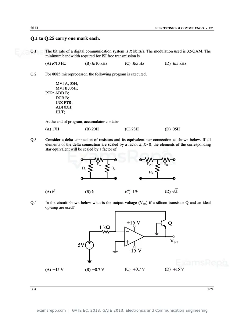
Text of page 41
2013                                                                       ELECTRONICS & COMMN. ENGG. - EC


Q.1 to Q.25 carry one mark each.

Q.1    The bit rate of a digital communication system is R kbits/s. The modulation used is 32-QAM. The
       minimum bandwidth required for ISI free transmission is
       (A) R/10 Hz             (B) R/10 kHz           (C) R/5 Hz                (D) R/5 kHz

Q.2    For 8085 microprocessor, the following program is executed.

            MVI A, 05H;
            MVI B, 05H;
       PTR: ADD B;
            DCR B;
            JNZ PTR;
            ADI 03H;
            HLT;

       At the end of program, accumulator contains
       (A) 17H                 (B) 20H                (C) 23H                   (D) 05H

Q.3    Consider a delta connection of resistors and its equivalent star connection as shown below. If all
       elements of the delta connection are scaled by a factor k, k> 0, the elements of the corresponding
       star equivalent will be scaled by a factor of


                                       Ra                            RC        RB
                            Rb                  Rc
                                                                      RA


       (A) k2                  (B) k                  (C) 1/k                   (D)     k

Q.4    In the circuit shown below what is the output voltage (Vout) if a silicon transistor Q and an ideal
       op-amp are used?


                                                       +15 V                        Q
                                         1 kΩ
                                                       –
                                                       +                            Vout
                          5V
                                                       – 15 V


       (A)      15 V           (B)     0.7 V          (C)    0.7 V              (D)     15 V


EC-C                                                                                                    2/24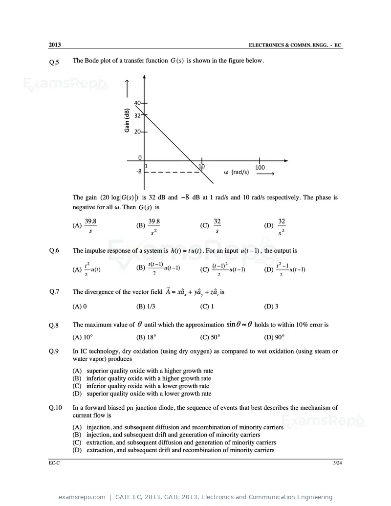
Text of page 42
2013                                                                                            ELECTRONICS & COMMN. ENGG. - EC


Q.5    The Bode plot of a transfer function G (s ) is shown in the figure below.


                            Gain (dB)


       The gain (20 log G ( s) ) is 32 dB and −8 dB at 1 rad/s and 10 rad/s respectively. The phase is
       negative for all ω. Then G (s) is

             39.8                             39.8                        32                                 32
       (A)                              (B)                         (C)                              (D)
              s                                s   2                       s                                 s2

Q.6    The impulse response of a system is h(t ) = t u (t ) . For an input u (t − 1) , the output is

             t2                               t (t −1)                    (t −1) 2                         t 2 −1
       (A)        u (t )                (B)              u (t −1)   (C)              u (t −1)        (D)            u (t −1)
             2                                  2                           2                                2

                                                          r
Q.7    The divergence of the vector field A = xaˆ x + yaˆ y + zaˆ z is

       (A) 0                            (B) 1/3                     (C) 1                            (D) 3

Q.8    The maximum value of θ until which the approximation sin θ ≈ θ holds to within 10% error is
       (A) 10°                          (B) 18°                     (C) 50°                          (D) 90°

Q.9    In IC technology, dry oxidation (using dry oxygen) as compared to wet oxidation (using steam or
       water vapor) produces
       (A)   superior quality oxide with a higher growth rate
       (B)   inferior quality oxide with a higher growth rate
       (C)   inferior quality oxide with a lower growth rate
       (D)   superior quality oxide with a lower growth rate

Q.10   In a forward biased pn junction diode, the sequence of events that best describes the mechanism of
       current flow is
       (A)   injection, and subsequent diffusion and recombination of minority carriers
       (B)   injection, and subsequent drift and generation of minority carriers
       (C)   extraction, and subsequent diffusion and generation of minority carriers
       (D)   extraction, and subsequent drift and recombination of minority carriers
EC-C                                                                                                                           3/24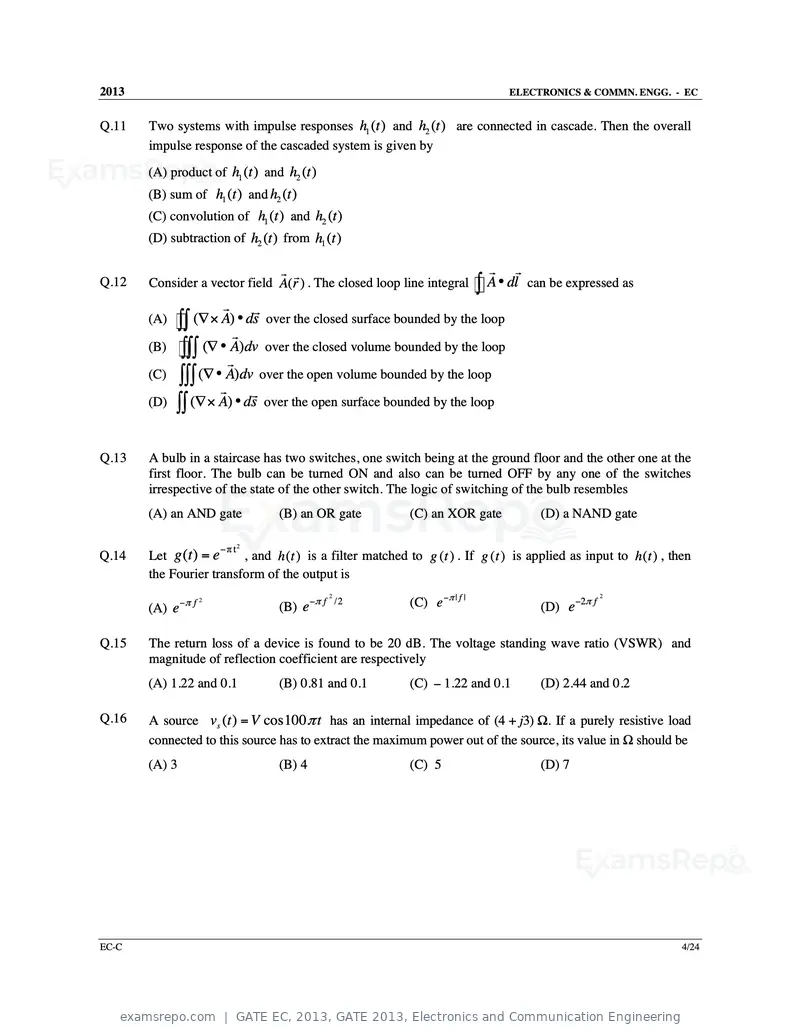
Text of page 43
2013                                                                              ELECTRONICS & COMMN. ENGG. - EC


Q.11   Two systems with impulse responses h1 (t ) and h2 (t ) are connected in cascade. Then the overall
       impulse response of the cascaded system is given by
       (A) product of h1 (t ) and h2 (t )
       (B) sum of h1 (t ) and h2 (t )
       (C) convolution of h1 (t ) and h2 (t )
       (D) subtraction of h2 (t ) from h1 (t )

                               r r                                            r   r
Q.12   Consider a vector field A( r ) . The closed loop line integral       ∫ A • dl can be expressed as
                        r        r
       (A) ∫∫ (∇× A)r• ds over the closed surface bounded by the loop
       (B) ∫∫∫ (∇ • A)dv over the closed volume bounded by the loop
                     r
       (C) ∫∫∫ (∇ • A)dv over the open volume bounded by the loop
                   r     r
       (D) ∫∫ (∇ × A) • ds over the open surface bounded by the loop


Q.13   A bulb in a staircase has two switches, one switch being at the ground floor and the other one at the
       first floor. The bulb can be turned ON and also can be turned OFF by any one of the switches
       irrespective of the state of the other switch. The logic of switching of the bulb resembles
       (A) an AND gate               (B) an OR gate        (C) an XOR gate             (D) a NAND gate

                        − π t2
Q.14   Let g (t ) = e    , and h (t ) is a filter matched to g (t ) . If g (t ) is applied as input to h (t ) , then
       the Fourier transform of the output is

                                                           (C) e −π | f |
                                              2                                                     2

       (A) e −π f                    (B) e−π f /2                                      (D) e−2π f
                    2


Q.15   The return loss of a device is found to be 20 dB. The voltage standing wave ratio (VSWR) and
       magnitude of reflection coefficient are respectively
       (A) 1.22 and 0.1              (B) 0.81 and 0.1      (C) − 1.22 and 0.1          (D) 2.44 and 0.2

Q.16   A source vs (t ) = V cos100 π t has an internal impedance of (4 + j3) Ω. If a purely resistive load
       connected to this source has to extract the maximum power out of the source, its value in Ω should be
       (A) 3                         (B) 4                 (C) 5                       (D) 7


EC-C                                                                                                              4/24
Text of page 44
2013 ELECTRONICS & COMMN. ENGG. - EC
V2 ( s )
Q.17 The transfer function of the circuit shown below is
V1 ( s )
0.5 s + 1 3s + 6
(A) (B)
s +1 s+2
s+2 s +1
(C) (D)
s +1 s+2
Q.18 Assuming zero initial condition, the response y (t ) of the system given below to a unit step input
u (t ) is
2
(A) u (t ) (B) t u (t ) (C) t u (t )
2
(D) e − t u (t )
A polynomial f ( x) = a4 x + a3 x + a2 x + a1 x − a0 with all coefficients positive has
4 3 2
Q.19
(A) no real roots (B) no negative real root
(C) odd number of real roots (D) at least one positive and one negative real root
Q.20 The minimum eigenvalue of the following matrix is
3 5 2
5 12 7
2 7 5
(A) 0 (B) 1 (C) 2 (D) 3
Q.21 Which one of the following statements is NOT TRUE for a continuous time causal and stable
LTI system?
(A) All the poles of the system must lie on the left side of the jω axis.
(B) Zeros of the system can lie anywhere in the s-plane.
(C) All the poles must lie within s = 1 .
(D) All the roots of the characteristic equation must be located on the left side of the jω axis.
EC-C 5/24
Text of page 45
2013                                                                              ELECTRONICS & COMMN. ENGG. - EC


Q.22   In a MOSFET operating in the saturation region, the channel length modulation effect causes
       (A)   an increase in the gate-source capacitance
       (B)   a decrease in the transconductance
       (C)   a decrease in the unity-gain cutoff frequency
       (D)   a decrease in the output resistance

Q.23   A band-limited signal with a maximum frequency of 5 kHz is to be sampled. According to the
       sampling theorem, the sampling frequency which is not valid is
       (A) 5 kHz                  (B) 12 kHz                 (C) 15 kHz                 (D) 20 kHz


Q.24   In a voltage-voltage feedback as shown below, which one of the following statements is TRUE if
       the gain k is increased?


       (A) The input impedance increases and output impedance decreases.
       (B) The input impedance increases and output impedance also increases.
       (C) The input impedance decreases and output impedance also decreases.
       (D) The input impedance decreases and output impedance increases.


Q.25   For a periodic signal v (t ) = 30 sin 100 t + 10 cos 300 t + 6 sin (500 t + π / 4) , the fundamental frequency in
       rad/s is
       (A) 100                    (B) 300                    (C) 500                    (D) 1500


EC-C                                                                                                                  6/24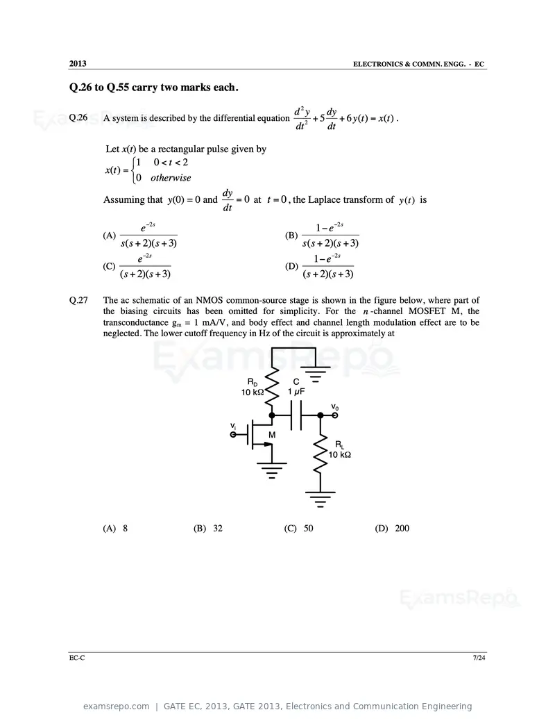
Text of page 46
2013 ELECTRONICS & COMMN. ENGG. - EC
Q.26 to Q.55 carry two marks each.
d2y dy
Q.26 A system is described by the differential equation 2
+ 5 + 6 y (t ) = x(t ) .
dt dt
Let x(t) be a rectangular pulse given by
1 0 < t < 2
x (t ) =
0 otherwise
dy
Assuming that y(0) = 0 and = 0 at t = 0 , the Laplace transform of y ( t ) is
dt
e−2 s 1 − e−2 s
(A) (B)
s ( s + 2)( s + 3) s ( s + 2)( s + 3)
e−2s 1 − e−2 s
(C) (D)
(s + 2)(s + 3) (s + 2)(s + 3)
Q.27 The ac schematic of an NMOS common-source stage is shown in the figure below, where part of
the biasing circuits has been omitted for simplicity. For the n -channel MOSFET M, the
transconductance gm = 1 mA/V, and body effect and channel length modulation effect are to be
neglected. The lower cutoff frequency in Hz of the circuit is approximately at
RD C
10 kΩ 1 µF
v0
vi
M
RL
10 kΩ
(A) 8 (B) 32 (C) 50 (D) 200
EC-C 7/24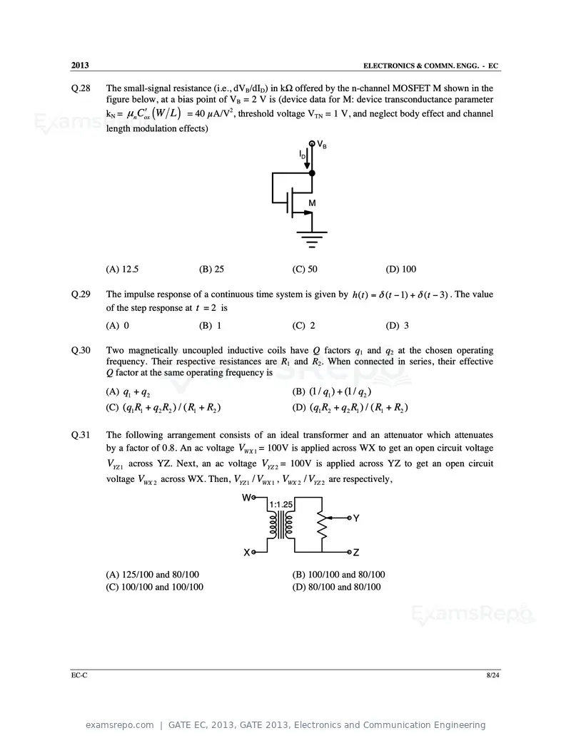
Text of page 47
2013                                                                          ELECTRONICS & COMMN. ENGG. - EC


Q.28   The small-signal resistance (i.e., dVB/dID) in kΩ offered by the n-channel MOSFET M shown in the
       figure below, at a bias point of VB = 2 V is (device data for M: device transconductance parameter
       kN = µn C ′ox (W L ) = 40 µA/V2, threshold voltage VTN = 1 V, and neglect body effect and channel
       length modulation effects)
                                                                    VB
                                                           ID


                                                                M


       (A) 12.5                    (B) 25               (C) 50                      (D) 100

Q.29   The impulse response of a continuous time system is given by h (t ) = δ (t − 1) + δ (t − 3) . The value
       of the step response at t = 2 is
       (A) 0                       (B) 1                (C) 2                       (D) 3

Q.30   Two magnetically uncoupled inductive coils have Q factors q1 and q2 at the chosen operating
       frequency. Their respective resistances are R1 and R2. When connected in series, their effective
       Q factor at the same operating frequency is
       (A) q1 + q2                                      (B) (1/ q1 ) + (1/ q2 )
       (C) ( q1 R1 + q2 R2 ) / ( R1 + R2 )              (D) ( q1 R2 + q2 R1 ) / ( R1 + R2 )

Q.31   The following arrangement consists of an ideal transformer and an attenuator which attenuates
       by a factor of 0.8. An ac voltage VWX 1 = 100V is applied across WX to get an open circuit voltage
       VYZ 1 across YZ. Next, an ac voltage VYZ 2 = 100V is applied across YZ to get an open circuit
       voltage VWX 2 across WX. Then, VYZ 1 / VWX 1 , VWX 2 / VYZ 2 are respectively,
                                             W
                                                  1:1.25
                                                                          Y


                                             X                            Z

       (A) 125/100 and 80/100                           (B) 100/100 and 80/100
       (C) 100/100 and 100/100                          (D) 80/100 and 80/100


EC-C                                                                                                        8/24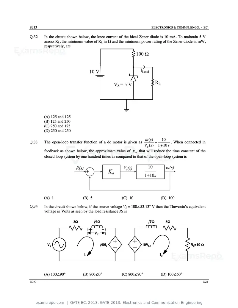
Text of page 48
2013                                                                      ELECTRONICS & COMMN. ENGG. - EC


Q.32   In the circuit shown below, the knee current of the ideal Zener diode is 10 mA. To maintain 5 V
       across RL, the minimum value of RL in Ω and the minimum power rating of the Zener diode in mW,
       respectively, are


       (A) 125 and 125
       (B) 125 and 250
       (C) 250 and 125
       (D) 250 and 250

                                                                    ω (s)       10
Q.33   The open-loop transfer function of a dc motor is given as             =        . When connected in
                                                                   V a ( s ) 1 + 10 s
       feedback as shown below, the approximate value of K a that will reduce the time constant of the
       closed loop system by one hundred times as compared to that of the open-loop system is


       (A) 1                  (B) 5                   (C) 10                     (D) 100

Q.34   In the circuit shown below, if the source voltage VS = 100∠53.13° V then the Thevenin’s equivalent
       voltage in Volts as seen by the load resistance RL is

                         3Ω           j4 Ω                            j6 Ω            5Ω


                                      VL1


        VS                                  j40I2                 10VL1                        RL=10 Ω

                               I1                                                I2


       (A) 100∠90°            (B) 800∠0°              (C) 800∠90°                (D) 100∠60°
EC-C                                                                                                   9/24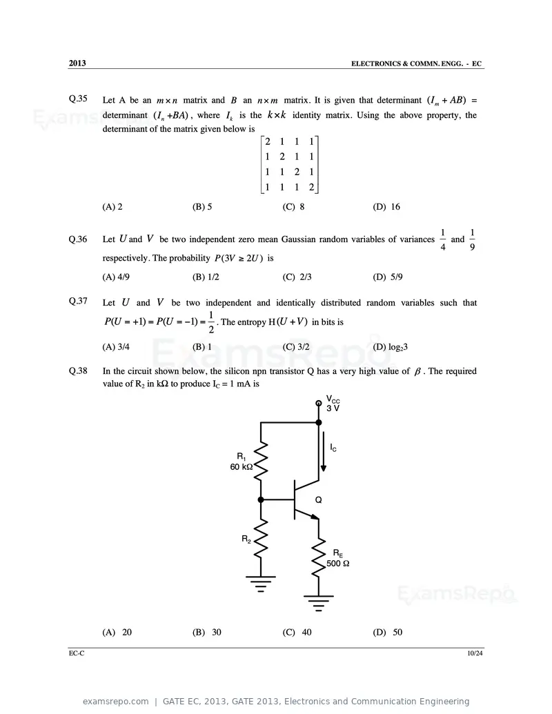
Text of page 49
2013 ELECTRONICS & COMMN. ENGG. - EC
Q.35 Let A be an m × n matrix and B an n × m matrix. It is given that determinant ( I m + AB ) =
determinant ( I n +BA) , where I k is the k × k identity matrix. Using the above property, the
determinant of the matrix given below is
2 1 1 1
1 2 1 1
1 1 2 1
1 1 1 2
(A) 2 (B) 5 (C) 8 (D) 16
1 1
Q.36 Let U and V be two independent zero mean Gaussian random variables of variances and
4 9
respectively. The probability P (3V ≥ 2U ) is
(A) 4/9 (B) 1/2 (C) 2/3 (D) 5/9
Q.37 Let U and V be two independent and identically distributed random variables such that
1
P(U = +1) = P(U = −1) = . The entropy H (U + V ) in bits is
2
(A) 3/4 (B) 1 (C) 3/2 (D) log23
Q.38 In the circuit shown below, the silicon npn transistor Q has a very high value of β . The required
value of R2 in kΩ to produce IC = 1 mA is
VCC
3V
IC
R1
60 kΩ
Q
R2
RE
500 Ω
(A) 20 (B) 30 (C) 40 (D) 50
EC-C 10/24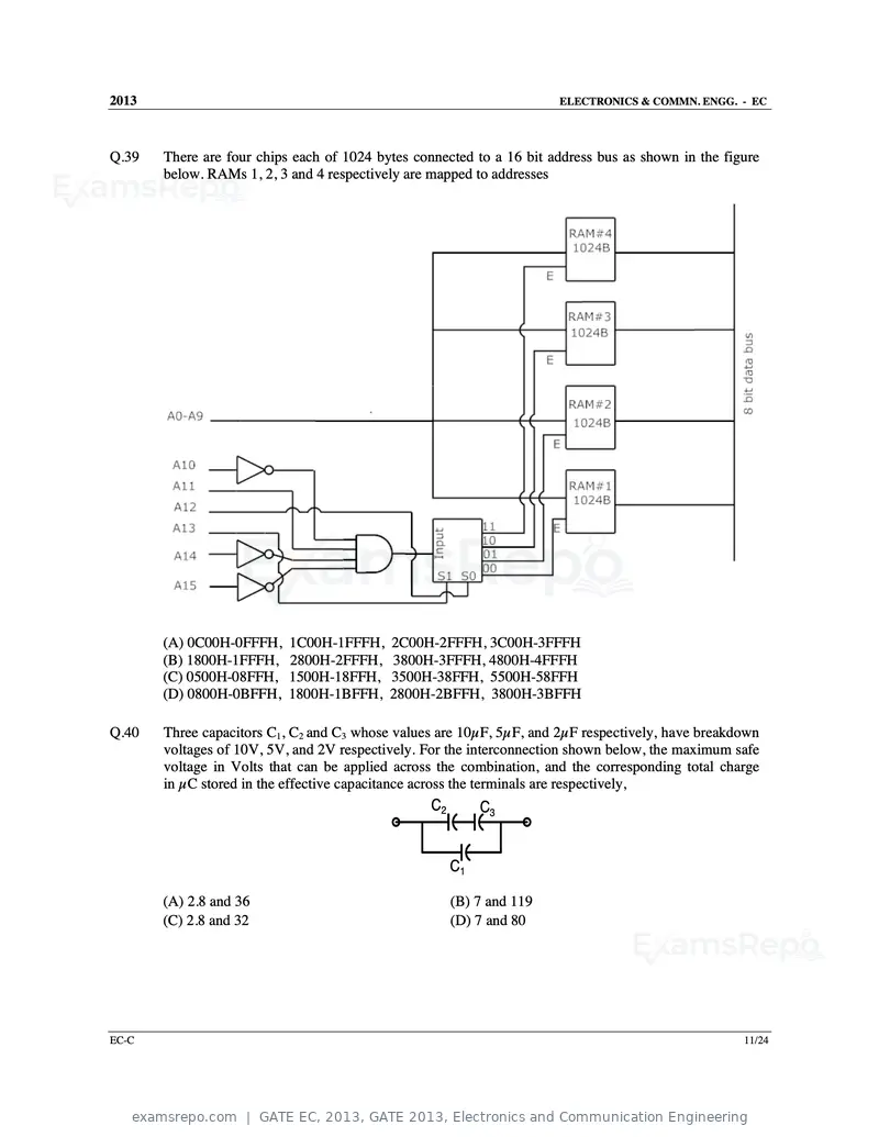
Text of page 50
2013                                                                   ELECTRONICS & COMMN. ENGG. - EC


Q.39   There are four chips each of 1024 bytes connected to a 16 bit address bus as shown in the figure
       below. RAMs 1, 2, 3 and 4 respectively are mapped to addresses


       (A) 0C00H-0FFFH, 1C00H-1FFFH, 2C00H-2FFFH, 3C00H-3FFFH
       (B) 1800H-1FFFH, 2800H-2FFFH, 3800H-3FFFH, 4800H-4FFFH
       (C) 0500H-08FFH, 1500H-18FFH, 3500H-38FFH, 5500H-58FFH
       (D) 0800H-0BFFH, 1800H-1BFFH, 2800H-2BFFH, 3800H-3BFFH

Q.40   Three capacitors C1, C2 and C3 whose values are 10µF, 5µF, and 2µF respectively, have breakdown
       voltages of 10V, 5V, and 2V respectively. For the interconnection shown below, the maximum safe
       voltage in Volts that can be applied across the combination, and the corresponding total charge
       in µC stored in the effective capacitance across the terminals are respectively,
                                                  C2        C3


                                                       C1

       (A) 2.8 and 36                                  (B) 7 and 119
       (C) 2.8 and 32                                  (D) 7 and 80


EC-C                                                                                                11/24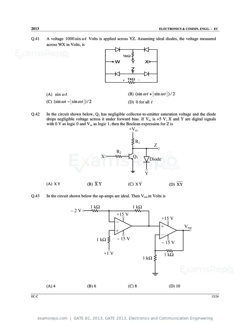
Text of page 51
2013                                                                      ELECTRONICS & COMMN. ENGG. - EC


Q.41   A voltage 1000 sin ω t Volts is applied across YZ. Assuming ideal diodes, the voltage measured
       across WX in Volts, is

                                                    1kΩ
                                               W          Y         X
                                                          Z

                                                    +   1kΩ     _


       (A) sin ω t                                      (B) (sin ω t + sin ω t ) / 2
       (C) (sin ω t − sin ω t ) / 2                     (D) 0 for all t

Q.42   In the circuit shown below, Q1 has negligible collector-to-emitter saturation voltage and the diode
       drops negligible voltage across it under forward bias. If Vcc is +5 V, X and Y are digital signals
       with 0 V as logic 0 and Vcc as logic 1, then the Boolean expression for Z is


       (A) X Y                  (B) X Y                 (C) X Y                  (D) XY

Q.43   In the circuit shown below the op-amps are ideal. Then Vout in Volts is


       (A) 4                    (B) 6                   (C) 8                    (D) 10

EC-C                                                                                                   12/24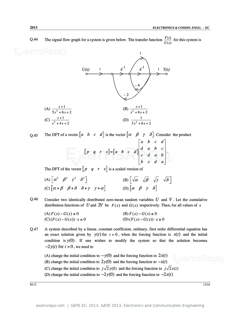
Text of page 52
2013 ELECTRONICS & COMMN. ENGG. - EC
Y (s)
Q.44 The signal flow graph for a system is given below. The transfer function for this system is
U ( s)
1
U(s) 1 s-1 s-1 1 Y(s)
–4
–2
s +1 s +1
(A) (B)
5s + 6s + 2
2
s + 6s + 2
2
s +1 1
(C) (D)
s2 + 4 s + 2 5s2 + 6s + 2
Q.45 The DFT of a vector [ a b c d ] is the vector [α β γ δ ] . Consider the product
a b c d
d a b c
[p q r s] = [a b c d ]
c
.
d a b
b c d a
The DFT of the vector [ p q r s ] is a scaled version of
(A) α 2 β 2 γ 2 δ 2 (B) α β γ δ
(C) [α + β β + δ δ + γ γ + α ] (D) [α β γ δ]
Q.46 Consider two identically distributed zero-mean random variables U and V . Let the cumulative
distribution functions of U and 2V be F ( x ) and G ( x ) respectively. Then, for all values of x
(A) F ( x ) − G ( x ) ≤ 0 (B) F ( x ) − G ( x ) ≥ 0
(C) ( F ( x ) − G ( x )) ⋅ x ≤ 0 (D) ( F ( x ) − G ( x )) ⋅ x ≥ 0
Q.47 A system described by a linear, constant coefficient, ordinary, first order differential equation has
an exact solution given by y (t ) for t > 0 , when the forcing function is x(t ) and the initial
condition is y (0) . If one wishes to modify the system so that the solution becomes
−2 y(t ) for t > 0 , we need to
(A) change the initial condition to − y(0) and the forcing function to 2 x(t )
(B) change the initial condition to 2 y (0) and the forcing function to − x(t )
(C) change the initial condition to j 2 y (0) and the forcing function to j 2 x ( t )
(D) change the initial condition to −2 y (0) and the forcing function to −2 x(t )
EC-C 13/24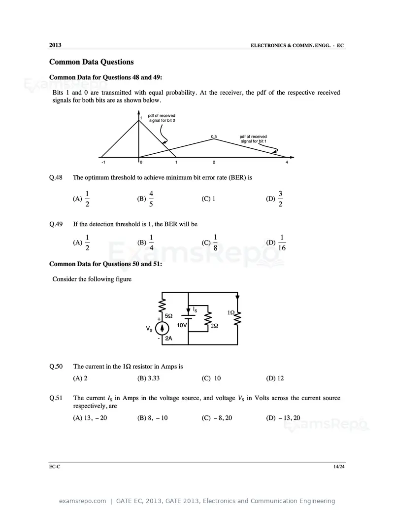
Text of page 53
2013                                                                                         ELECTRONICS & COMMN. ENGG. - EC


Common Data Questions
Common Data for Questions 48 and 49:

 Bits 1 and 0 are transmitted with equal probability. At the receiver, the pdf of the respective received
 signals for both bits are as shown below.

                                       pdf of received
                                 1
                                        signal for bit 0


                                                                            0.5        pdf of received
                                                                                        signal for bit 1


                   -1            0                         1                2                                     4


Q.48    The optimum threshold to achieve minimum bit error rate (BER) is

              1                        4                                                                     3
        (A)                      (B)                                  (C) 1                            (D)
              2                        5                                                                     2

Q.49    If the detection threshold is 1, the BER will be

              1                        1                                     1                                1
        (A)                      (B)                                  (C)                              (D)
              2                        4                                     8                               16

Common Data for Questions 50 and 51:

 Consider the following figure


                                                                 IS
                                                                                  1Ω
                                            + 5Ω
                                     VS
                                                           10V              2Ω

                                             - 2A


Q.50    The current in the 1Ω resistor in Amps is
        (A) 2                    (B) 3.33                             (C) 10                           (D) 12

Q.51    The current IS in Amps in the voltage source, and voltage VS in Volts across the current source
        respectively, are
        (A) 13, − 20             (B) 8, − 10                          (C) − 8, 20                      (D) − 13, 20


EC-C                                                                                                                    14/24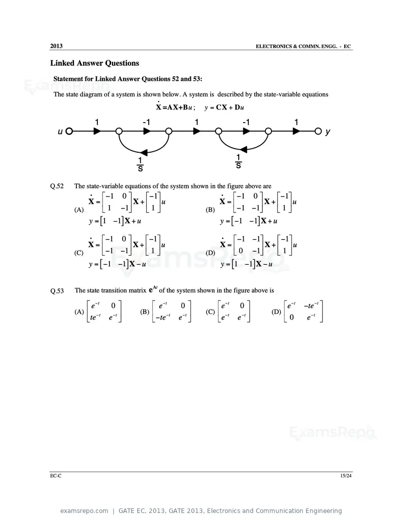
Text of page 54
2013 ELECTRONICS & COMMN. ENGG. - EC
Linked Answer Questions
Statement for Linked Answer Questions 52 and 53:
The state diagram of a system is shown below. A system is described by the state-variable equations
•
X =AX+B u ; y = CX + D u
1 -1 1 -1 1
u y
1 1
s s
Q.52 The state-variable equations of the system shown in the figure above are
• −1 0 −1 • −1 0 −1
X= X+ u X= X+ u
(A) 1 −1 1 (B) −1 −1 1
y = [1 −1] X + u y = [ −1 −1] X + u
• −1 0 −1 • −1 −1 −1
X= X + 1 u X= X + 1 u
(C) −1 −1 (D) 0 −1
y = [ −1 −1] X − u y = [1 −1] X − u
At
Q.53 The state transition matrix e of the system shown in the figure above is
e −t 0 e−t 0 e−t 0 e −t −te − t
(A) − t (B) (C) − t (D)
te e −t −te
−t
e−t e e −t 0 e−t
EC-C 15/24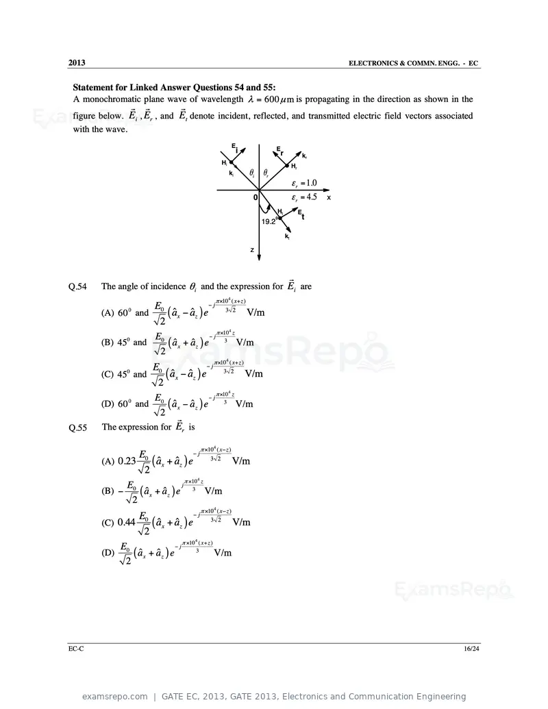
Text of page 55
2013                                                                                                                ELECTRONICS & COMMN. ENGG. - EC


 Statement for Linked Answer Questions 54 and 55:
 A monochromatic plane wave of wavelength λ = 600 µ m is propagating in the direction as shown in the
                 r r              r
 figure below. Ei , Er , and Et denote incident, reflected, and transmitted electric field vectors associated
 with the wave.
                                                                   E
                                                                    i                E
                                                                                         r                 kr
                                                          Hi
                                                                                                  Hr
                                                               ki        θi θr
                                                                                                  ε r = 1.0
                                                                          0                       ε r = 4.5     x
                                                                                     Ht                E
                                                                                     0                 t
                                                                              19.2
                                                                                             kt

                                                                         z


                                                                                                  r
Q.54    The angle of incidence θ i and the expression for Ei are
                                                      π ×104 ( x + z )
                     E                   −j
        (A) 60 0 and 0 ( aˆ x − aˆ z ) e        3 2
                                                    V/m
                      2
                                            π ×10 z            4
                     E0                  −j
        (B) 450 and     ( aˆ x + aˆ z ) e 3 V/m
                      2
                                                     π ×104 ( x + z )
                     E                  −j
        (C) 450 and 0 ( aˆ x − aˆ z ) e        3 2
                                                      V/m
                      2
                                            π ×10 z            4
                     E                   −j
        (D) 60 0 and 0 ( aˆ x − aˆ z ) e       3
                                                    V/m
                       2
                            r
Q.55    The expression for Er is

                                               π ×104 ( x − z )
                 E                     −j
        (A) 0.23 0 ( aˆ x + aˆ z ) e       3 2
                                               V/m
                  2
                                   π ×10 z 4
              E
        (B) − 0 ( aˆ x + aˆ z ) e 3 V/m
                                 j

               2
                                               π ×104 ( x − z )
                 E                     −j
        (C) 0.44 0 ( aˆ x + aˆ z ) e             3 2
                                                       V/m
                    2
                                   π ×10 ( x + z )
                                       4
             E                  −j
        (D) 0 ( aˆ x + aˆ z ) e         3
                                                   V/m
              2


EC-C                                                                                                                                           16/24
Text of page 56
2013                                                                       ELECTRONICS & COMMN. ENGG. - EC


General Aptitude (GA) Questions
Q.56 to Q.60 carry one mark each.
 Q.56   Complete the sentence:
        Dare _______________ mistakes.
        (A) commit              (B) to commit            (C) committed          (D) committing

 Q.57   They were requested not to quarrel with others.
        Which one of the following options is the closest in meaning to the word quarrel?
        (A) make out            (B) call out             (C) dig out            (D) fall out

 Q.58   Statement: You can always give me a ring whenever you need.
        Which one of the following is the best inference from the above statement?
        (A) Because I have a nice caller tune.
        (B) Because I have a better telephone facility.
        (C) Because a friend in need is a friend indeed.
        (D) Because you need not pay towards the telephone bills when you give me a ring.

 Q.59   In the summer of 2012, in New Delhi, the mean temperature of Monday to Wednesday was 41°C
        and of Tuesday to Thursday was 43°C. If the temperature on Thursday was 15% higher than that of
        Monday, then the temperature in °C on Thursday was
        (A) 40                  (B) 43                   (C) 46                 (D) 49

 Q.60   Choose the grammatically CORRECT sentence:
        (A) Two and two add four.
        (B) Two and two become four.
        (C) Two and two are four.
        (D) Two and two make four.
Q.61 to Q.65 carry two marks each.
 Q.61   The set of values of p for which the roots of the equation 3x2+2x+p(p–1) = 0 are of opposite sign is
        (A) (–∞, 0)             (B) (0, 1)               (C) (1, ∞)             (D) (0, ∞)

 Q.62   What is the chance that a leap year, selected at random, will contain 53 Saturdays?
        (A) 2/7                 (B) 3/7                  (C) 1/7                (D) 5/7

 Q.63   Find the sum to n terms of the series 10+84+ 734 + .....

        (A)
              (
            9 9n + 1  )
                     +1
               10
        (B)
              (
            9 9n − 1  )
                     +1
               8
        (C)
              (
            9 9n −1   )
                     +n
               8
        (D)
              (
            9 9n − 1  )
                     + n2
                8
EC-C                                                                                                      17/24
Text of page 57
2013                                                                       ELECTRONICS & COMMN. ENGG. - EC


 Q.64   Statement: There were different streams of freedom movements in colonial India carried out by the
        moderates, liberals, radicals, socialists, and so on.
        Which one of the following is the best inference from the above statement?
        (A) The emergence of nationalism in colonial India led to our Independence.
        (B) Nationalism in India emerged in the context of colonialism.
        (C) Nationalism in India is homogeneous.
        (D) Nationalism in India is heterogeneous.

 Q.65   A car travels 8 km in the first quarter of an hour, 6 km in the second quarter and 16 km in the third
        quarter. The average speed of the car in km per hour over the entire journey is
        (A) 30                  (B) 36                  (C) 40                   (D) 24


                              END OF THE QUESTION PAPER


EC-C                                                                                                      18/24
Text of page 58
SESSION - 4
Text of page 59
2013                                                                      Question Booklet Code
                                                                                                         D
         EC : ELECTRONICS AND COMMUNICATION ENGINEERING
Duration: Three Hours                                                                     Maximum Marks: 100

Read the following instructions carefully.

    1. Do not open the seal of the Question Booklet until you are asked to do so by the invigilator.
    2. Take out the Optical Response Sheet (ORS) from this Question Booklet without breaking the seal
        and read the instructions printed on the ORS carefully. If you find that either:
        a. The Question Booklet Code printed at the right hand top corner of this page does not match with
             the Question Booklet Code at the right hand top corner of the ORS or
        b. The Question Paper Code preceding the Registration number on the ORS is not EC,
       then exchange the booklet immediately with a new sealed Question Booklet.
    3. On the right hand side of the ORS, using ONLY a black ink ballpoint pen, (i) darken the appropriate
       bubble under each digit of your registration number and (ii) write your registration number, your
       name and name of the examination centre and put your signature at the specified location.
    4. This Question Booklet contains 24 pages including blank pages for rough work. After you are
       permitted to open the seal, check all pages and report discrepancies, if any, to the invigilator.
    5. There are a total of 65 questions carrying 100 marks. All these questions are of objective type. Each
       question has only one correct answer. Questions must be answered on the left hand side of the ORS
       by darkening the appropriate bubble (marked A, B, C, D) using ONLY a black ink ballpoint pen
       against the question number. For each question darken the bubble of the correct answer. More
       than one answer bubbled against a question will be treated as an incorrect response.
    6. Since bubbles darkened by the black ink ballpoint pen cannot be erased, candidates should darken the
       bubbles in the ORS very carefully.
    7. Questions Q.1 – Q.25 carry 1 mark each. Questions Q.26 – Q.55 carry 2 marks each. The 2 marks
       questions include two pairs of common data questions and two pairs of linked answer questions. The
       answer to the second question of the linked answer questions depends on the answer to the first
       question of the pair. If the first question in the linked pair is wrongly answered or is not attempted,
       then the answer to the second question in the pair will not be evaluated.
    8. Questions Q.56 – Q.65 belong to General Aptitude (GA) section and carry a total of 15 marks.
       Questions Q.56 – Q.60 carry 1 mark each, and questions Q.61 – Q.65 carry 2 marks each.
    9. Questions not attempted will result in zero mark and wrong answers will result in NEGATIVE
       marks. For all 1 mark questions, ⅓ mark will be deducted for each wrong answer. For all 2 marks
       questions, ⅔ mark will be deducted for each wrong answer. However, in the case of the linked
       answer question pair, there will be negative marks only for wrong answer to the first question and no
       negative marks for wrong answer to the second question.
    10. Calculator is allowed whereas charts, graph sheets or tables are NOT allowed in the examination hall.
    11. Rough work can be done on the Question Booklet itself. Blank pages are provided at the end of the
        Question Booklet for rough work.
    12. Before the start of the examination, write your name and registration number in the space provided
        below using a black ink ballpoint pen.

           Name

           Registration Number         EC

EC-D                                                                                                      1/24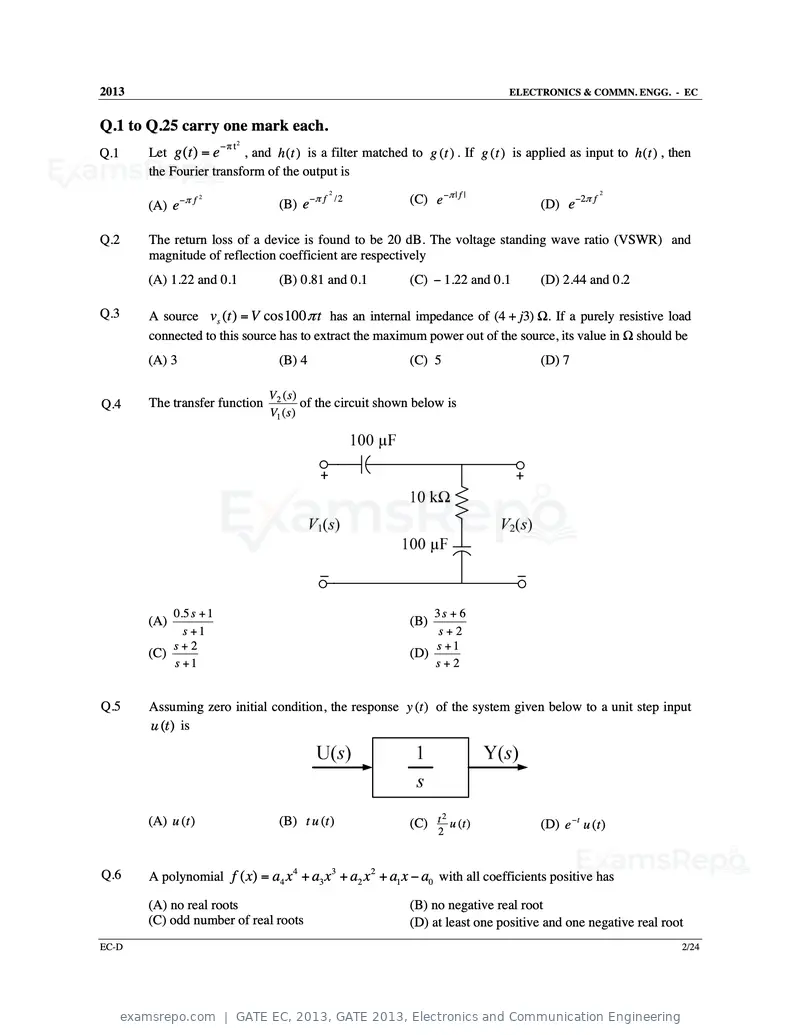
Text of page 60
2013                                                                           ELECTRONICS & COMMN. ENGG. - EC


Q.1 to Q.25 carry one mark each.
                        − π t2
Q.1    Let g (t ) = e    , and h (t ) is a filter matched to g (t ) . If g (t ) is applied as input to h (t ) , then
       the Fourier transform of the output is

                                                             (C) e −π | f |
                                             2                                                     2

       (A) e −π f                  (B) e−π f /2                                      (D) e−2π f
                    2


Q.2    The return loss of a device is found to be 20 dB. The voltage standing wave ratio (VSWR) and
       magnitude of reflection coefficient are respectively
       (A) 1.22 and 0.1            (B) 0.81 and 0.1          (C) − 1.22 and 0.1      (D) 2.44 and 0.2

Q.3    A source vs (t ) = V cos100 π t has an internal impedance of (4 + j3) Ω. If a purely resistive load
       connected to this source has to extract the maximum power out of the source, its value in Ω should be
       (A) 3                       (B) 4                     (C) 5                   (D) 7

                                 V2 ( s )
Q.4    The transfer function              of the circuit shown below is
                                 V1 ( s )


           0.5 s + 1                                             3s + 6
       (A)                                                   (B)
             s +1                                                 s+2
           s+2                                                   s +1
       (C)                                                   (D)
           s +1                                                  s+2


Q.5    Assuming zero initial condition, the response y (t ) of the system given below to a unit step input
       u (t ) is


                                                                  2
       (A) u (t )                  (B) t u (t )              (C) t u (t )
                                                                    2
                                                                                     (D) e − t u (t )


       A polynomial f ( x) = a4 x + a3 x + a2 x + a1 x − a0 with all coefficients positive has
                                      4       3       2
Q.6

       (A) no real roots                                     (B) no negative real root
       (C) odd number of real roots                          (D) at least one positive and one negative real root
EC-D                                                                                                              2/24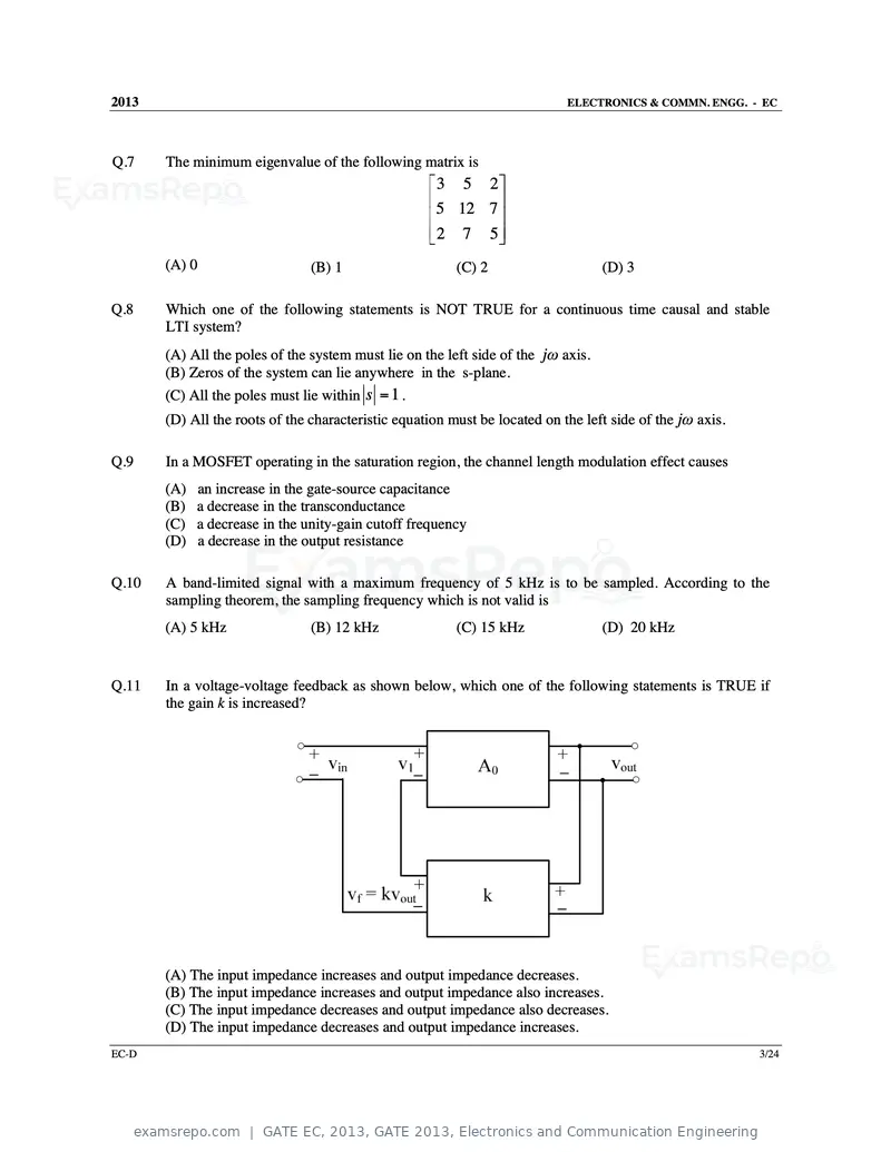
Text of page 61
2013 ELECTRONICS & COMMN. ENGG. - EC
Q.7 The minimum eigenvalue of the following matrix is
3 5 2
5 12 7
2 7 5
(A) 0 (B) 1 (C) 2 (D) 3
Q.8 Which one of the following statements is NOT TRUE for a continuous time causal and stable
LTI system?
(A) All the poles of the system must lie on the left side of the jω axis.
(B) Zeros of the system can lie anywhere in the s-plane.
(C) All the poles must lie within s = 1 .
(D) All the roots of the characteristic equation must be located on the left side of the jω axis.
Q.9 In a MOSFET operating in the saturation region, the channel length modulation effect causes
(A) an increase in the gate-source capacitance
(B) a decrease in the transconductance
(C) a decrease in the unity-gain cutoff frequency
(D) a decrease in the output resistance
Q.10 A band-limited signal with a maximum frequency of 5 kHz is to be sampled. According to the
sampling theorem, the sampling frequency which is not valid is
(A) 5 kHz (B) 12 kHz (C) 15 kHz (D) 20 kHz
Q.11 In a voltage-voltage feedback as shown below, which one of the following statements is TRUE if
the gain k is increased?
(A) The input impedance increases and output impedance decreases.
(B) The input impedance increases and output impedance also increases.
(C) The input impedance decreases and output impedance also decreases.
(D) The input impedance decreases and output impedance increases.
EC-D 3/24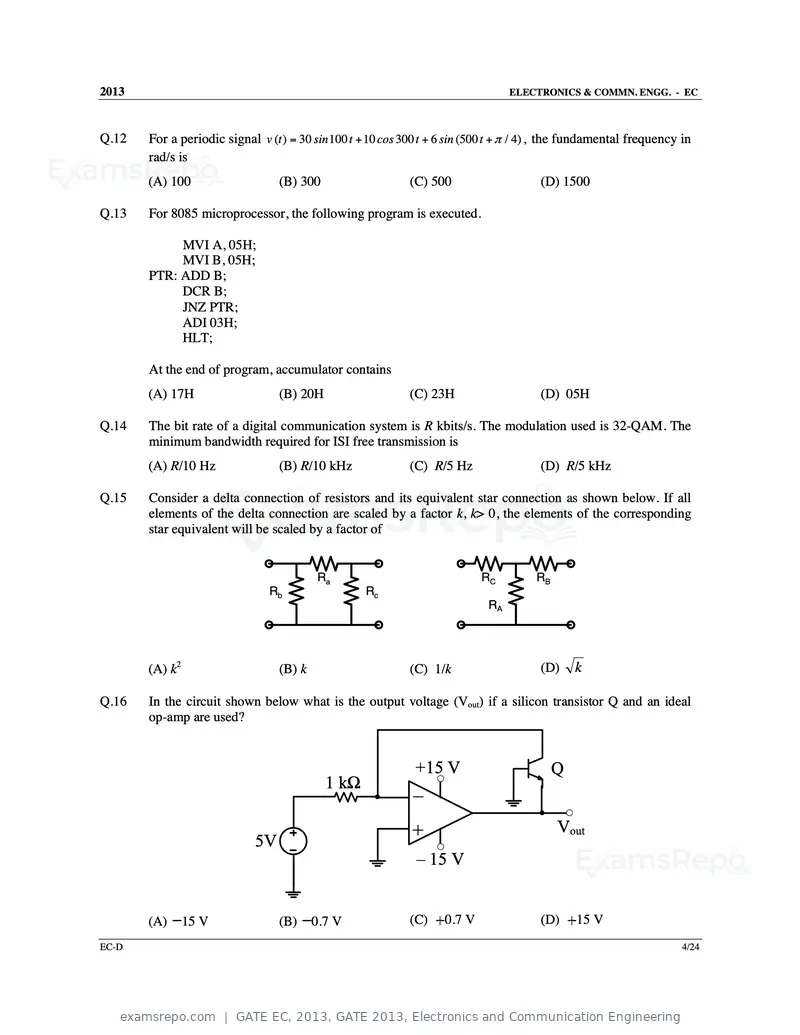
Text of page 62
2013                                                                              ELECTRONICS & COMMN. ENGG. - EC


Q.12   For a periodic signal v (t ) = 30 sin 100 t + 10 cos 300 t + 6 sin (500 t + π / 4) , the fundamental frequency in
       rad/s is
       (A) 100                    (B) 300                    (C) 500                    (D) 1500

Q.13   For 8085 microprocessor, the following program is executed.

            MVI A, 05H;
            MVI B, 05H;
       PTR: ADD B;
            DCR B;
            JNZ PTR;
            ADI 03H;
            HLT;

       At the end of program, accumulator contains
       (A) 17H                    (B) 20H                    (C) 23H                    (D) 05H

Q.14   The bit rate of a digital communication system is R kbits/s. The modulation used is 32-QAM. The
       minimum bandwidth required for ISI free transmission is
       (A) R/10 Hz                (B) R/10 kHz               (C) R/5 Hz                 (D) R/5 kHz

Q.15   Consider a delta connection of resistors and its equivalent star connection as shown below. If all
       elements of the delta connection are scaled by a factor k, k> 0, the elements of the corresponding
       star equivalent will be scaled by a factor of


                                          Ra                                RC         RB
                                Rb                  Rc
                                                                             RA


       (A) k2                     (B) k                      (C) 1/k                    (D)     k

Q.16   In the circuit shown below what is the output voltage (Vout) if a silicon transistor Q and an ideal
       op-amp are used?


                                                              +15 V                         Q
                                            1 kΩ
                                                              –
                                                             +                              Vout
                             5V
                                                              – 15 V


       (A)      15 V              (B)     0.7 V              (C)    0.7 V               (D)     15 V
EC-D                                                                                                                  4/24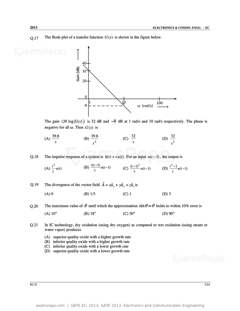
Text of page 63
2013                                                                                            ELECTRONICS & COMMN. ENGG. - EC


Q.17   The Bode plot of a transfer function G (s ) is shown in the figure below.


                            Gain (dB)


       The gain (20 log G ( s) ) is 32 dB and −8 dB at 1 rad/s and 10 rad/s respectively. The phase is
       negative for all ω. Then G (s) is

             39.8                             39.8                        32                                 32
       (A)                              (B)                         (C)                              (D)
              s                                s   2                       s                                 s2


Q.18   The impulse response of a system is h(t ) = t u (t ) . For an input u (t − 1) , the output is

             t2                               t (t −1)                    (t −1) 2                         t 2 −1
       (A)        u (t )                (B)              u (t −1)   (C)              u (t −1)        (D)            u (t −1)
             2                                  2                           2                                2


                                                          r
Q.19   The divergence of the vector field A = xaˆ x + yaˆ y + zaˆ z is

       (A) 0                            (B) 1/3                     (C) 1                            (D) 3


Q.20   The maximum value of θ until which the approximation sin θ ≈ θ holds to within 10% error is
       (A) 10°                          (B) 18°                     (C) 50°                          (D) 90°

Q.21   In IC technology, dry oxidation (using dry oxygen) as compared to wet oxidation (using steam or
       water vapor) produces
       (A)   superior quality oxide with a higher growth rate
       (B)   inferior quality oxide with a higher growth rate
       (C)   inferior quality oxide with a lower growth rate
       (D)   superior quality oxide with a lower growth rate


EC-D                                                                                                                           5/24
Text of page 64
2013                                                                         ELECTRONICS & COMMN. ENGG. - EC


Q.22   In a forward biased pn junction diode, the sequence of events that best describes the mechanism of
       current flow is
       (A)   injection, and subsequent diffusion and recombination of minority carriers
       (B)   injection, and subsequent drift and generation of minority carriers
       (C)   extraction, and subsequent diffusion and generation of minority carriers
       (D)   extraction, and subsequent drift and recombination of minority carriers

Q.23   Two systems with impulse responses h1 (t ) and h2 (t ) are connected in cascade. Then the overall
       impulse response of the cascaded system is given by
       (A) product of h1 (t ) and h2 (t )
       (B) sum of h1 (t ) and h2 (t )
       (C) convolution of h1 (t ) and h2 (t )
       (D) subtraction of h2 (t ) from h1 (t )


Q.24   A bulb in a staircase has two switches, one switch being at the ground floor and the other one at the
       first floor. The bulb can be turned ON and also can be turned OFF by any one of the switches
       irrespective of the state of the other switch. The logic of switching of the bulb resembles
       (A) an AND gate           (B) an OR gate          (C) an XOR gate          (D) a NAND gate

                               r r                                       r r
Q.25   Consider a vector field A( r ) . The closed loop line integral   ∫ • dl can be expressed as
                                                                         A
                   r      r
       (A) ∫∫  (∇× A ) • ds over the closed surface bounded by the loop
                      r
       (B) ∫∫∫ (∇ • A)dv over the closed volume bounded by the loop
                     r
       (C) ∫∫∫ (∇ • A)dv over the open volume bounded by the loop
                   r      r
       (D) ∫∫ (∇× A) • ds over the open surface bounded by the loop


EC-D                                                                                                      6/24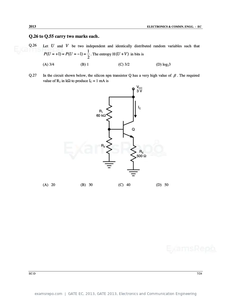
Text of page 65
2013                                                                        ELECTRONICS & COMMN. ENGG. - EC


Q.26 to Q.55 carry two marks each.
Q.26   Let U and V be two independent and identically distributed random variables such that
                              1
       P(U = +1) = P(U = −1) = . The entropy H (U + V ) in bits is
                              2
       (A) 3/4                (B) 1                   (C) 3/2                    (D) log23

Q.27   In the circuit shown below, the silicon npn transistor Q has a very high value of β . The required
       value of R2 in kΩ to produce IC = 1 mA is
                                                                    VCC
                                                                    3V


                                                                    IC
                                         R1
                                        60 kΩ


                                                                Q


                                           R2
                                                                     RE
                                                                    500 Ω


       (A) 20                 (B) 30                  (C) 40                     (D) 50


EC-D                                                                                                    7/24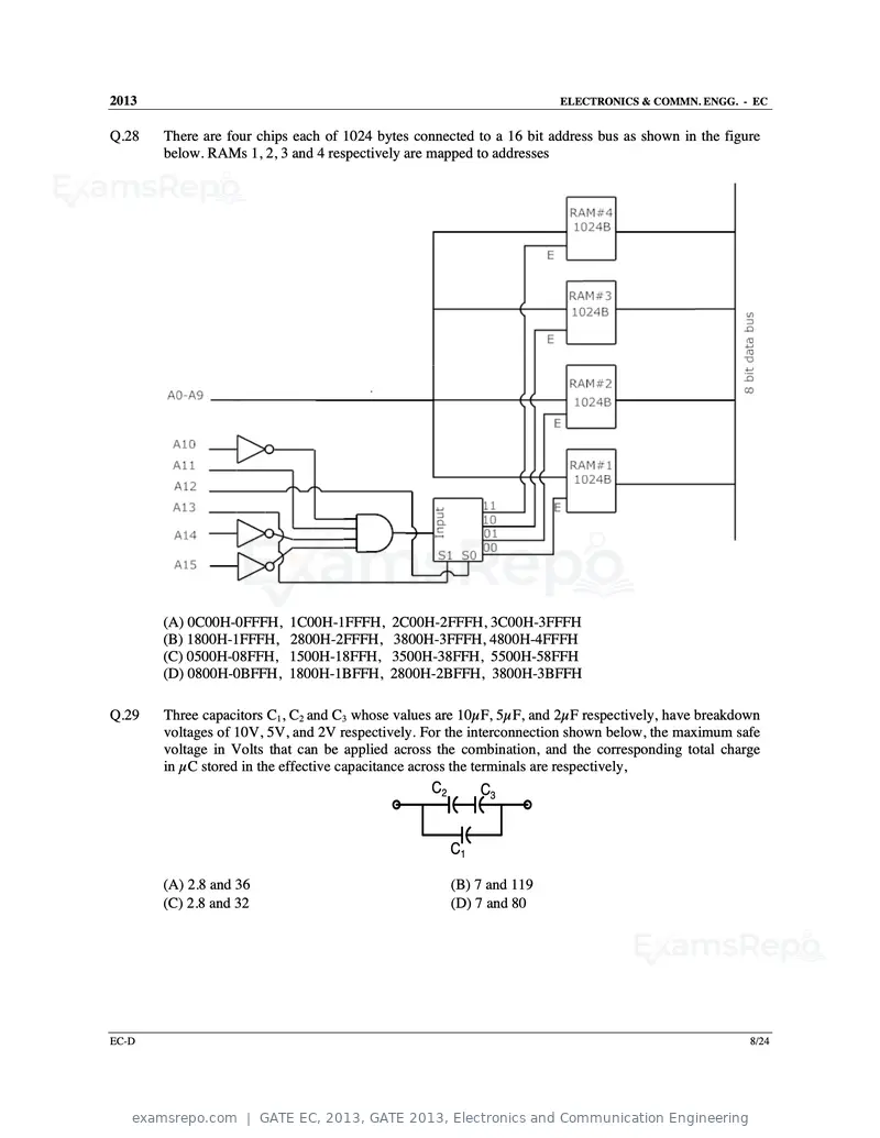
Text of page 66
2013                                                                   ELECTRONICS & COMMN. ENGG. - EC


Q.28   There are four chips each of 1024 bytes connected to a 16 bit address bus as shown in the figure
       below. RAMs 1, 2, 3 and 4 respectively are mapped to addresses


       (A) 0C00H-0FFFH, 1C00H-1FFFH, 2C00H-2FFFH, 3C00H-3FFFH
       (B) 1800H-1FFFH, 2800H-2FFFH, 3800H-3FFFH, 4800H-4FFFH
       (C) 0500H-08FFH, 1500H-18FFH, 3500H-38FFH, 5500H-58FFH
       (D) 0800H-0BFFH, 1800H-1BFFH, 2800H-2BFFH, 3800H-3BFFH

Q.29   Three capacitors C1, C2 and C3 whose values are 10µF, 5µF, and 2µF respectively, have breakdown
       voltages of 10V, 5V, and 2V respectively. For the interconnection shown below, the maximum safe
       voltage in Volts that can be applied across the combination, and the corresponding total charge
       in µC stored in the effective capacitance across the terminals are respectively,
                                                  C2        C3


                                                       C1

       (A) 2.8 and 36                                  (B) 7 and 119
       (C) 2.8 and 32                                  (D) 7 and 80


EC-D                                                                                                 8/24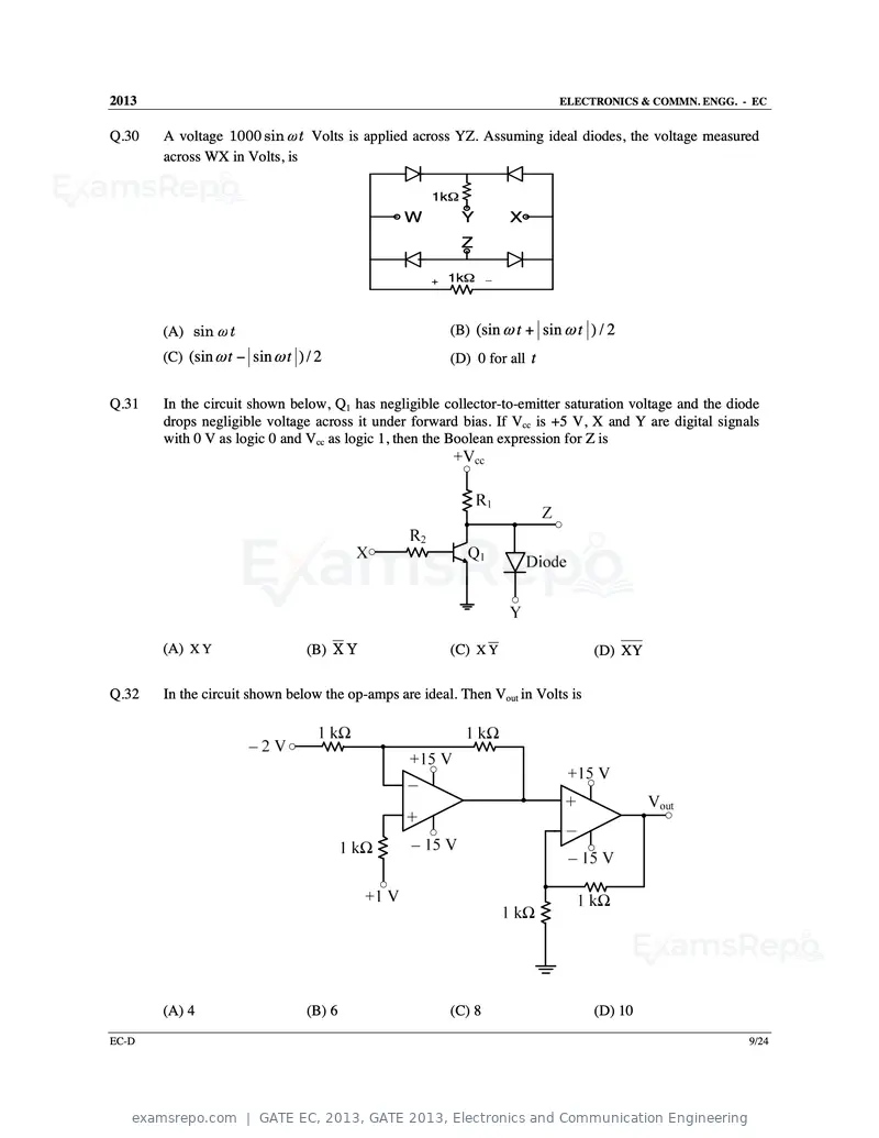
Text of page 67
2013                                                                      ELECTRONICS & COMMN. ENGG. - EC


Q.30   A voltage 1000 sin ω t Volts is applied across YZ. Assuming ideal diodes, the voltage measured
       across WX in Volts, is

                                                    1kΩ
                                               W          Y         X
                                                          Z

                                                    +   1kΩ     _


       (A) sin ω t                                      (B) (sin ω t + sin ω t ) / 2
       (C) (sin ω t − sin ω t ) / 2                     (D) 0 for all t


Q.31   In the circuit shown below, Q1 has negligible collector-to-emitter saturation voltage and the diode
       drops negligible voltage across it under forward bias. If Vcc is +5 V, X and Y are digital signals
       with 0 V as logic 0 and Vcc as logic 1, then the Boolean expression for Z is


       (A) X Y                  (B) X Y                 (C) X Y                  (D) XY

Q.32   In the circuit shown below the op-amps are ideal. Then Vout in Volts is


       (A) 4                    (B) 6                   (C) 8                    (D) 10
EC-D                                                                                                    9/24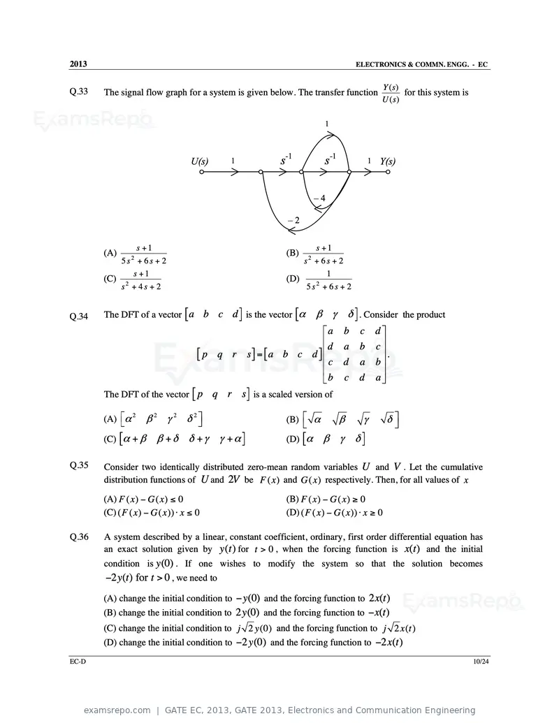
Text of page 68
2013 ELECTRONICS & COMMN. ENGG. - EC
Y (s)
Q.33 The signal flow graph for a system is given below. The transfer function for this system is
U ( s)
1
U(s) 1 s-1 s-1 1 Y(s)
–4
–2
s +1 s +1
(A) (B)
5s + 6s + 2
2
s + 6s + 2
2
s +1 1
(C) (D)
s2 + 4 s + 2 5s2 + 6s + 2
Q.34 The DFT of a vector [ a b c d ] is the vector [α β γ δ ] . Consider the product
a b c d
d a b c
[p q r s] = [a b c d ]
c
.
d a b
b c d a
The DFT of the vector [ p q r s ] is a scaled version of
(A) α β 2 γ 2 δ 2 (B) α β γ δ
2
(C) [α + β β + δ δ + γ γ + α ] (D) [α β γ δ]
Q.35 Consider two identically distributed zero-mean random variables U and V . Let the cumulative
distribution functions of U and 2V be F ( x ) and G ( x ) respectively. Then, for all values of x
(A) F ( x ) − G ( x ) ≤ 0 (B) F ( x ) − G ( x ) ≥ 0
(C) ( F ( x ) − G ( x )) ⋅ x ≤ 0 (D) ( F ( x ) − G ( x )) ⋅ x ≥ 0
Q.36 A system described by a linear, constant coefficient, ordinary, first order differential equation has
an exact solution given by y (t ) for t > 0 , when the forcing function is x(t ) and the initial
condition is y (0) . If one wishes to modify the system so that the solution becomes
−2 y(t ) for t > 0 , we need to
(A) change the initial condition to − y(0) and the forcing function to 2 x(t )
(B) change the initial condition to 2 y (0) and the forcing function to − x(t )
(C) change the initial condition to j 2 y (0) and the forcing function to j 2 x ( t )
(D) change the initial condition to −2 y (0) and the forcing function to −2 x(t )
EC-D 10/24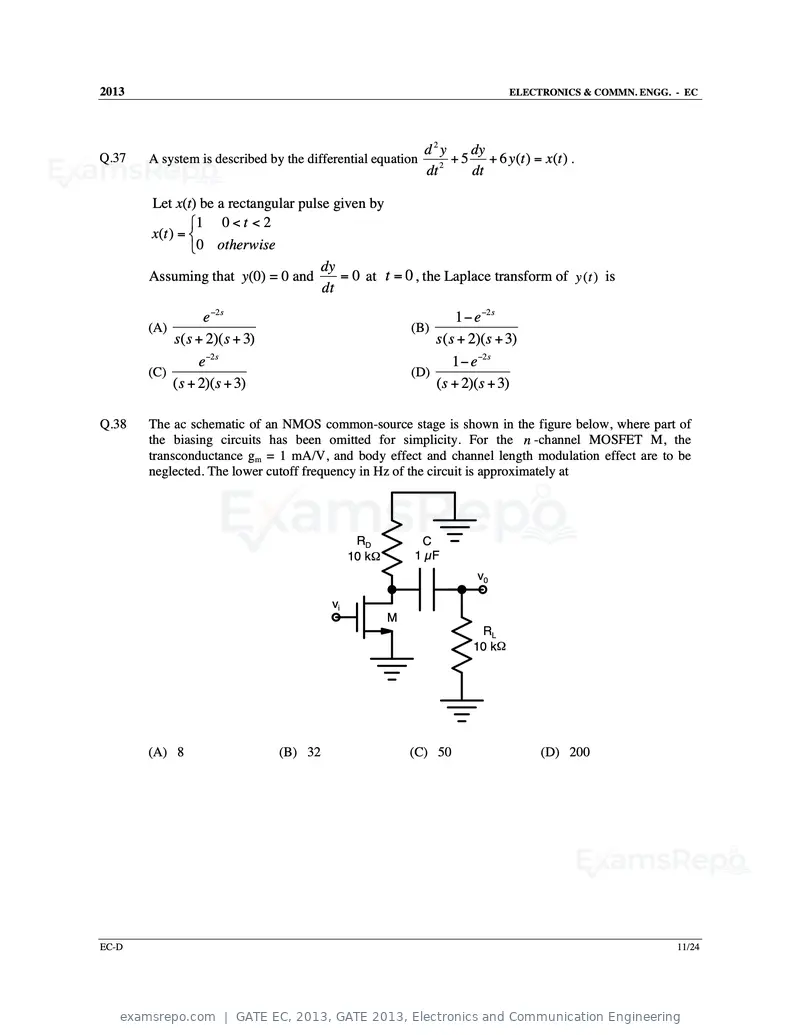
Text of page 69
2013 ELECTRONICS & COMMN. ENGG. - EC
d2y dy
Q.37 A system is described by the differential equation 2
+ 5 + 6 y (t ) = x(t ) .
dt dt
Let x(t) be a rectangular pulse given by
1 0 < t < 2
x (t ) =
0 otherwise
dy
Assuming that y(0) = 0 and = 0 at t = 0 , the Laplace transform of y ( t ) is
dt
e−2 s 1 − e−2 s
(A) (B)
s ( s + 2)( s + 3) s ( s + 2)( s + 3)
e−2s 1 − e−2 s
(C) (D)
(s + 2)(s + 3) (s + 2)(s + 3)
Q.38 The ac schematic of an NMOS common-source stage is shown in the figure below, where part of
the biasing circuits has been omitted for simplicity. For the n -channel MOSFET M, the
transconductance gm = 1 mA/V, and body effect and channel length modulation effect are to be
neglected. The lower cutoff frequency in Hz of the circuit is approximately at
RD C
10 kΩ 1 µF
v0
vi
M
RL
10 kΩ
(A) 8 (B) 32 (C) 50 (D) 200
EC-D 11/24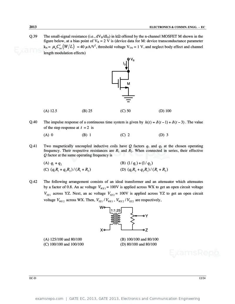
Text of page 70
2013                                                                          ELECTRONICS & COMMN. ENGG. - EC


Q.39   The small-signal resistance (i.e., dVB/dID) in kΩ offered by the n-channel MOSFET M shown in the
       figure below, at a bias point of VB = 2 V is (device data for M: device transconductance parameter
       kN = µn C ′ox (W L ) = 40 µA/V2, threshold voltage VTN = 1 V, and neglect body effect and channel
       length modulation effects)
                                                                    VB
                                                           ID


                                                                M


       (A) 12.5                    (B) 25               (C) 50                      (D) 100

Q.40   The impulse response of a continuous time system is given by h (t ) = δ (t − 1) + δ (t − 3) . The value
       of the step response at t = 2 is
       (A) 0                       (B) 1                (C) 2                       (D) 3

Q.41   Two magnetically uncoupled inductive coils have Q factors q1 and q2 at the chosen operating
       frequency. Their respective resistances are R1 and R2. When connected in series, their effective
       Q factor at the same operating frequency is
       (A) q1 + q2                                      (B) (1/ q1 ) + (1/ q2 )
       (C) ( q1 R1 + q2 R2 ) / ( R1 + R2 )              (D) ( q1 R2 + q2 R1 ) / ( R1 + R2 )


Q.42   The following arrangement consists of an ideal transformer and an attenuator which attenuates
       by a factor of 0.8. An ac voltage VWX 1 = 100V is applied across WX to get an open circuit voltage
       VYZ 1 across YZ. Next, an ac voltage VYZ 2 = 100V is applied across YZ to get an open circuit
       voltage VWX 2 across WX. Then, VYZ 1 / VWX 1 , VWX 2 / VYZ 2 are respectively,
                                             W
                                                  1:1.25
                                                                          Y


                                             X                            Z

       (A) 125/100 and 80/100                           (B) 100/100 and 80/100
       (C) 100/100 and 100/100                          (D) 80/100 and 80/100


EC-D                                                                                                       12/24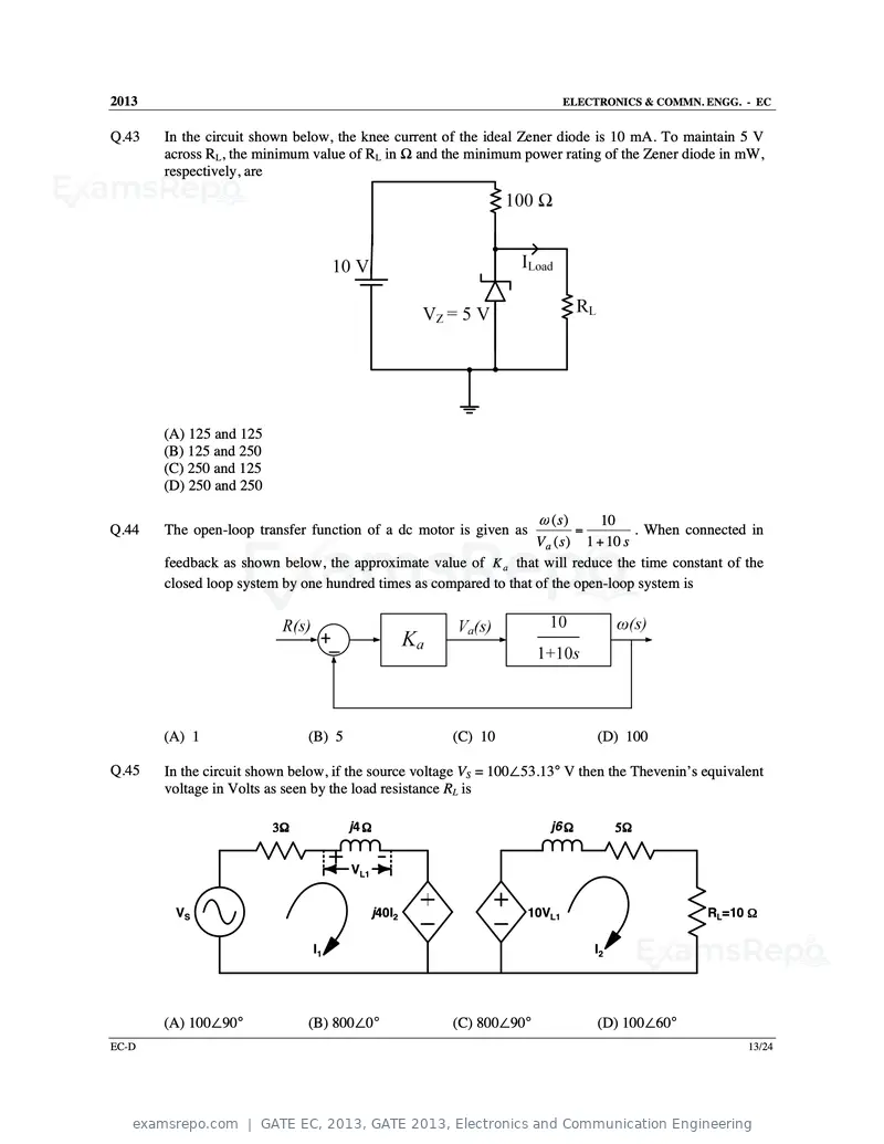
Text of page 71
2013                                                                      ELECTRONICS & COMMN. ENGG. - EC


Q.43   In the circuit shown below, the knee current of the ideal Zener diode is 10 mA. To maintain 5 V
       across RL, the minimum value of RL in Ω and the minimum power rating of the Zener diode in mW,
       respectively, are


       (A) 125 and 125
       (B) 125 and 250
       (C) 250 and 125
       (D) 250 and 250

                                                                    ω (s)     10
Q.44   The open-loop transfer function of a dc motor is given as             =      . When connected in
                                                                   Va ( s) 1 + 10 s
       feedback as shown below, the approximate value of K a that will reduce the time constant of the
       closed loop system by one hundred times as compared to that of the open-loop system is


       (A) 1                  (B) 5                   (C) 10                     (D) 100

Q.45   In the circuit shown below, if the source voltage VS = 100∠53.13° V then the Thevenin’s equivalent
       voltage in Volts as seen by the load resistance RL is

                         3Ω           j4 Ω                            j6 Ω            5Ω


                                      VL1


        VS                                  j40I2                 10VL1                        RL=10 Ω

                               I1                                                I2


       (A) 100∠90°            (B) 800∠0°              (C) 800∠90°                (D) 100∠60°
EC-D                                                                                                  13/24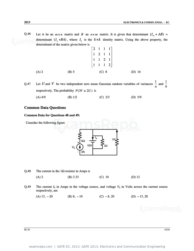
Text of page 72
2013 ELECTRONICS & COMMN. ENGG. - EC
Q.46 Let A be an m × n matrix and B an n × m matrix. It is given that determinant ( I m + AB ) =
determinant ( I n +BA) , where I k is the k × k identity matrix. Using the above property, the
determinant of the matrix given below is
2 1 1 1
1 2 1 1
1 1 2 1
1 1 1 2
(A) 2 (B) 5 (C) 8 (D) 16
1 1
Q.47 Let U and V be two independent zero mean Gaussian random variables of variances and
4 9
respectively. The probability P (3V ≥ 2U ) is
(A) 4/9 (B) 1/2 (C) 2/3 (D) 5/9
Common Data Questions
Common Data for Questions 48 and 49:
Consider the following figure
IS
1Ω
+ 5Ω
VS
10V 2Ω
- 2A
Q.48 The current in the 1Ω resistor in Amps is
(A) 2 (B) 3.33 (C) 10 (D) 12
Q.49 The current IS in Amps in the voltage source, and voltage VS in Volts across the current source
respectively, are
(A) 13, − 20 (B) 8, − 10 (C) − 8, 20 (D) − 13, 20
EC-D 14/24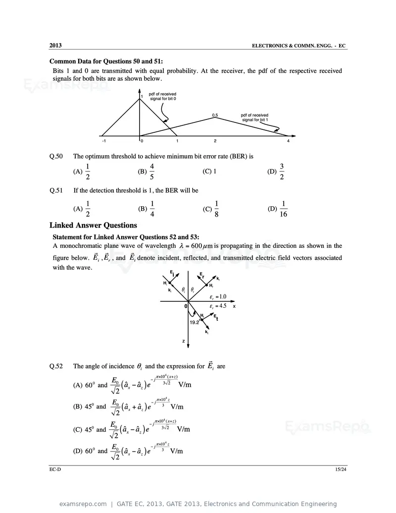
Text of page 73
2013                                                                                                                                   ELECTRONICS & COMMN. ENGG. - EC


Common Data for Questions 50 and 51:
 Bits 1 and 0 are transmitted with equal probability. At the receiver, the pdf of the respective received
 signals for both bits are as shown below.

                                                    pdf of received
                                                1
                                                     signal for bit 0


                                                                                                                0.5              pdf of received
                                                                                                                                  signal for bit 1


                          -1                    0                                 1                                 2                                      4


Q.50    The optimum threshold to achieve minimum bit error rate (BER) is
              1                                         4                                                                                              3
        (A)                                   (B)                                                     (C) 1                                      (D)
              2                                         5                                                                                              2
Q.51    If the detection threshold is 1, the BER will be

              1                                         1                                                           1                                   1
        (A)                                   (B)                                                     (C)                                        (D)
              2                                         4                                                           8                                  16
Linked Answer Questions
 Statement for Linked Answer Questions 52 and 53:
 A monochromatic plane wave of wavelength λ = 600 µ m is propagating in the direction as shown in the
                      r    r              r
 figure below. Ei , Er , and Et denote incident, reflected, and transmitted electric field vectors associated
 with the wave.
                                                                          E                       E
                                                                              i                       r                 kr
                                                                   Hi
                                                                                                               Hr
                                                                         ki           θi θ r
                                                                                                               ε r = 1.0
                                                                                       0                       ε r = 4.5     x
                                                                                                  Ht                E
                                                                                                  0                 t
                                                                                           19.2
                                                                                                          kt

                                                                                      z


                                                                                                               r
Q.52    The angle of incidence θ i and the expression for Ei are
                                                              π ×104 ( x + z )
                    E                   −j
        (A) 60 and 0 ( aˆ x − aˆ z ) e
                  0                            3 2
                                                   V/m
                     2
                                           π ×10 z                   4
                    E0                  −j
        (B) 450 and    ( aˆ x + aˆ z ) e 3 V/m
                     2
                                                             π ×104 ( x + z )
                               E0                       −j
        (C) 45 and0
                                    ( aˆ x − aˆ z ) e V/m         3 2

                     2
                                            π ×10 z                 4
                    E                    −j
        (D) 60 0 and 0 ( aˆ x − aˆ z ) e       3
                                                    V/m
                     2
EC-D                                                                                                                                                              15/24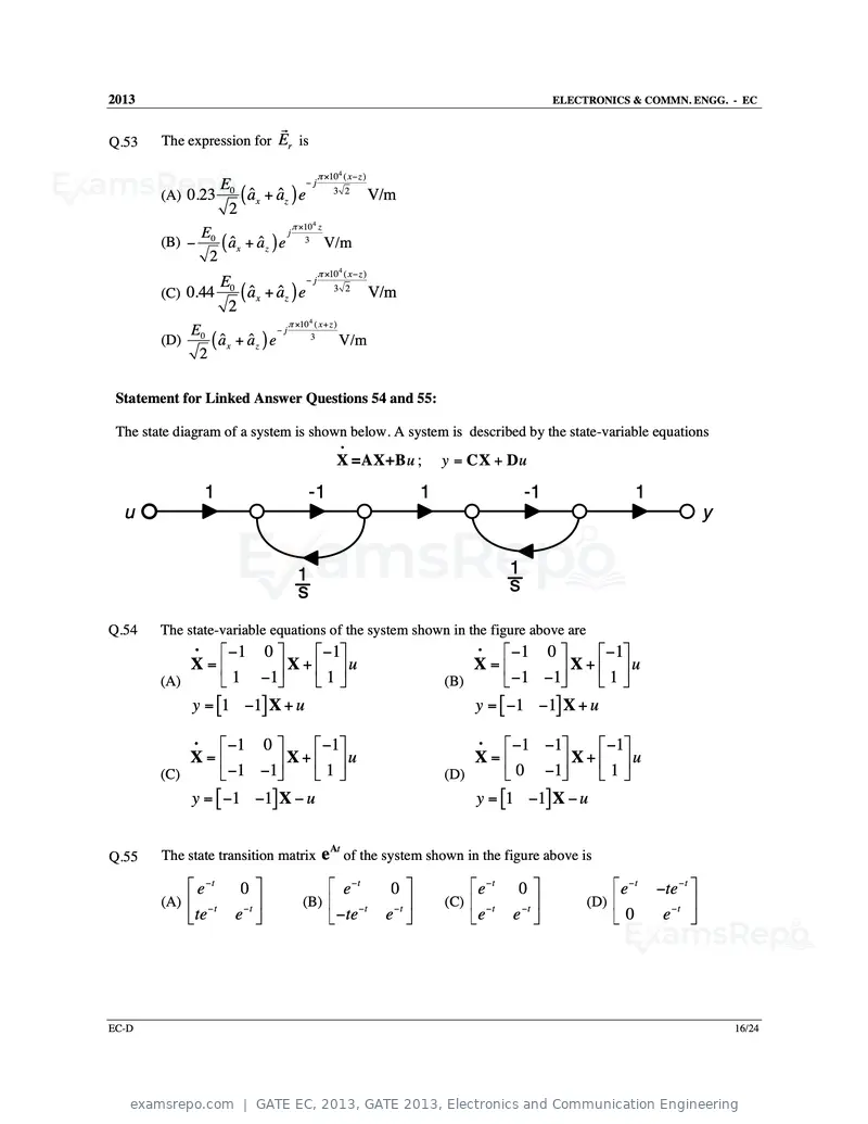
Text of page 74
2013 ELECTRONICS & COMMN. ENGG. - EC
r
Q.53 The expression for Er is
π ×104 ( x − z )
E0 −j
(A) 0.23 ( aˆx + aˆz ) e 3 2
V/m
2
π ×10 z 4
E
(B) − 0 ( aˆ x + aˆ z ) e 3 V/m
j
2
π ×104 ( x − z )
E0 −j
(C) 0.44 ( aˆ x + aˆz ) e 3 2
V/m
2
π ×10 ( x + z )4
E −j
(D) 0 ( aˆ x + aˆ z ) e 3
V/m
2
Statement for Linked Answer Questions 54 and 55:
The state diagram of a system is shown below. A system is described by the state-variable equations
•
X =AX+B u ; y = CX + D u
1 -1 1 -1 1
u y
1 1
s s
Q.54 The state-variable equations of the system shown in the figure above are
• −1 0 −1 • −1 0 −1
X= X+ u X= X+ u
(A) 1 −1 1 (B) −1 −1 1
y = [1 −1] X + u y = [ −1 −1] X + u
• −1 0 −1 • −1 −1 −1
X= X+ u X= X+ u
(C) −1 −1 1 (D) 0 −1 1
y = [ −1 −1] X − u y = [1 −1] X − u
At
Q.55 The state transition matrix e of the system shown in the figure above is
e −t 0 e−t 0 e−t 0 e −t −te − t
(A) −t (B) (C) − t (D)
te e −t −te
−t
e−t e e −t 0 e−t
EC-D 16/24
Text of page 75
2013                                                                      ELECTRONICS & COMMN. ENGG. - EC


General Aptitude (GA) Questions

Q.56 to Q.60 carry one mark each.

 Q.56   They were requested not to quarrel with others.
        Which one of the following options is the closest in meaning to the word quarrel?
        (A) make out             (B) call out           (C) dig out             (D) fall out

 Q.57   In the summer of 2012, in New Delhi, the mean temperature of Monday to Wednesday was 41°C
        and of Tuesday to Thursday was 43°C. If the temperature on Thursday was 15% higher than that of
        Monday, then the temperature in °C on Thursday was
        (A) 40                   (B) 43                 (C) 46                  (D) 49

 Q.58   Complete the sentence:
        Dare _______________ mistakes.
        (A) commit               (B) to commit          (C) committed           (D) committing

 Q.59   Choose the grammatically CORRECT sentence:
        (A) Two and two add four.
        (B) Two and two become four.
        (C) Two and two are four.
        (D) Two and two make four.

 Q.60   Statement: You can always give me a ring whenever you need.
        Which one of the following is the best inference from the above statement?
        (A) Because I have a nice caller tune.
        (B) Because I have a better telephone facility.
        (C) Because a friend in need is a friend indeed.
        (D) Because you need not pay towards the telephone bills when you give me a ring.


Q.61 to Q.65 carry two marks each.
 Q.61   What is the chance that a leap year, selected at random, will contain 53 Saturdays?
        (A) 2/7                  (B) 3/7                (C) 1/7                 (D) 5/7

 Q.62   Statement: There were different streams of freedom movements in colonial India carried out by the
        moderates, liberals, radicals, socialists, and so on.
        Which one of the following is the best inference from the above statement?
        (A) The emergence of nationalism in colonial India led to our Independence.
        (B) Nationalism in India emerged in the context of colonialism.
        (C) Nationalism in India is homogeneous.
        (D) Nationalism in India is heterogeneous.


EC-D                                                                                                  17/24
Text of page 76
2013                                                                       ELECTRONICS & COMMN. ENGG. - EC


 Q.63   The set of values of p for which the roots of the equation 3x2+2x+p(p–1) = 0 are of opposite sign is
        (A) (–∞, 0)             (B) (0, 1)               (C) (1, ∞)              (D) (0, ∞)

 Q.64   A car travels 8 km in the first quarter of an hour, 6 km in the second quarter and 16 km in the third
        quarter. The average speed of the car in km per hour over the entire journey is
        (A) 30                  (B) 36                   (C) 40                  (D) 24

 Q.65   Find the sum to n terms of the series 10+84+ 734 + .....

        (A)
              (
            9 9n + 1  )
                     +1
               10
        (B)
              (
            9 9n − 1  )
                     +1
               8
        (C)
              (
            9 9n −1   )
                     +n
               8
        (D)
              (
            9 9n − 1  )
                     + n2
                8

                              END OF THE QUESTION PAPER


EC-D                                                                                                      18/24
Official key not published for this paper.
Page 1 of 76
Source: GATE. Question paper published by GATE.