
GATE EC 2016: Electronics and Communication Engineering Session 1

Text of page 1
GATE 2016                                                                     General Aptitude - GA Set-1


Q. 1 – Q. 5 carry one mark each.
Q.1    Which of the following is CORRECT with respect to grammar and usage?

       Mount Everest is ____________.
      (A) the highest peak in the world

      (B) highest peak in the world

      (C) one of highest peak in the world

      (D) one of the highest peak in the world


Q.2    The policeman asked the victim of a theft, “What did you        ?”
      (A) loose                (B) lose                (C) loss                (D) louse


Q.3    Despite the new medicine’s ______________ in treating diabetes, it is not ______________widely.
      (A) effectiveness --- prescribed                 (B) availability --- used
      (C) prescription --- available                   (D) acceptance --- proscribed


Q.4    In a huge pile of apples and oranges, both ripe and unripe mixed together, 15% are unripe fruits. Of
       the unripe fruits, 45% are apples. Of the ripe ones, 66% are oranges. If the pile contains a total of
       5692000 fruits, how many of them are apples?

      (A) 2029198              (B) 2467482             (C) 2789080             (D) 3577422


Q.5    Michael lives 10 km away from where I live. Ahmed lives 5 km away and Susan lives 7 km away
       from where I live. Arun is farther away than Ahmed but closer than Susan from where I live. From
       the information provided here, what is one possible distance (in km) at which I live from Arun’s
       place?

      (A) 3.00                 (B) 4.99                (C) 6.02                (D) 7.01


Q. 6 – Q. 10 carry two marks each.

Q.6    A person moving through a tuberculosis prone zone has a 50% probability of becoming infected.
       However, only 30% of infected people develop the disease. What percentage of people moving
       through a tuberculosis prone zone remains infected but does not show symptoms of disease?

      (A) 15                   (B) 33                  (C) 35                  (D) 37


                                                                                                               1/2
Text of page 2
GATE 2016                                                                                  General Aptitude - GA Set-1

Q.7    In a world filled with uncertainty, he was glad to have many good friends. He had always assisted
       them in times of need and was confident that they would reciprocate. However, the events of the
       last week proved him wrong.

       Which of the following inference(s) is/are logically valid and can be inferred from the above
       passage?

         (i) His friends were always asking him to help them.

         (ii) He felt that when in need of help, his friends would let him down.

         (iii) He was sure that his friends would help him when in need.

         (iv) His friends did not help him last week.

       (A) (i) and (ii)             (B) (iii) and (iv)                (C) (iii) only          (D) (iv) only


Q.8    Leela is older than her cousin Pavithra. Pavithra’s brother Shiva is older than Leela. When Pavithra
       and Shiva are visiting Leela, all three like to play chess. Pavithra wins more often than Leela does.

       Which one of the following statements must be TRUE based on the above?
       (A) When Shiva plays chess with Leela and Pavithra, he often loses.

       (B) Leela is the oldest of the three.

       (C) Shiva is a better chess player than Pavithra.

       (D) Pavithra is the youngest of the three.


                     1                   1                   1
       If qq −aa =        and rr −bb =        and ss −cc =
Q.9
                                                                  , the value of abc is   .
                     rr                  ss                  qq


       (A) (rrrrrr)−1               (B) 0                             (C) 1                   (D) r+q+s


Q.10   P, Q, R and S are working on a project. Q can finish the task in 25 days, working alone for 12
       hours a day. R can finish the task in 50 days, working alone for 12 hours per day. Q worked 12
       hours a day but took sick leave in the beginning for two days. R worked 18 hours a day on all days.
       What is the ratio of work done by Q and R after 7 days from the start of the project?

       (A) 10:11                     (B) 11:10                           (C) 20:21                (D) 21:20


                                  END OF THE QUESTION PAPER


                                                                                                                             2/2
Text of page 3
GATE 2016 Electronics and Communication Engineering (Set 1)


Q. 1 – Q. 25 carry one mark each.
 Q.1     Let M4 = I, (where I denotes the identity matrix) and M ≠ I, M2 ≠ I and M3 ≠ I. Then, for any
         natural number k, M−1 equals:
         (A) M4k + 1               (B) M4k + 2               (C) M4k + 3               (D) M4k


 Q.2     The second moment of a Poisson-distributed random variable is 2. The mean of the random
         variable is _______


 Q.3     Given the following statements about a function f: ℝ → ℝ, select the right option:

         P: If f(x) is continuous at x = x0 , then it is also differentiable at x = x0 .
         Q: If f(x) is continuous at x = x0 , then it may not be differentiable at x = x0 .
         R: If f(x) is differentiable at x = x0 , then it is also continuous at x = x0 .

         (A) P is true, Q is false, R is false               (B) P is false, Q is true, R is true
         (C) P is false, Q is true, R is false               (D) P is true, Q is false, R is true


 Q.4     Which one of the following is a property of the solutions to the Laplace equation: ∇2 f = 0?
         (A) The solutions have neither maxima nor minima anywhere except at the boundaries.
         (B) The solutions are not separable in the coordinates.
         (C) The solutions are not continuous.
         (D) The solutions are not dependent on the boundary conditions.


EC (1)                                                                                                  1/17
Text of page 4
GATE 2016 Electronics and Communication Engineering (Set 1)


 Q.5     Consider the plot of f(x) versus x as shown below.


                            x
         Suppose F(x) = ∫−5 f(y)dy. Which one of the following is a graph of F(x)?


         (A)                                              (B)


         (C)                                              (D)


 Q.6     Which one of the following is an eigen function of the class of all continuous-time, linear, time-
         invariant systems (u(t) denotes the unit-step function)?
         (A) e jω0 t u(t)                                 (B) cos (ω0 t)

         (C) e jω0 t                                      (D) sin (ω0 t)


 Q.7     A continuous-time function x(t) is periodic with period T. The function is sampled uniformly with
         a sampling period Ts . In which one of the following cases is the sampled signal periodic?
         (A) T = √2 Ts                                    (B) T = 1.2 Ts
         (C) Always                                       (D) Never


 Q.8     Consider the sequence x[n] = an u[n] + b n u[n], where u[n] denotes the unit-step sequence and
         0 < |a| < |b| < 1. The region of convergence (ROC) of the z-transform of x[n] is
         (A) |z| > |a|           (B) |z| > |b|            (C) |z| < |a|           (D) |a| < |z| < |b|


EC (1)                                                                                                        2/17
Text of page 5
GATE 2016 Electronics and Communication Engineering (Set 1)


 Q.9                                                                    A      B
         Consider a two-port network with the transmission matrix: T = �         �. If the network is
                                                                        C      D
         reciprocal, then
         (A) T −1 = T                                    (B) T 2 = T
         (C) Determinant (T) = 0                         (D) Determinant (T) = 1


 Q.10    A continuous-time sinusoid of frequency 33 Hz is multiplied with a periodic Dirac impulse train of
         frequency 46 Hz. The resulting signal is passed through an ideal analog low-pass filter with a cutoff
         frequency of 23 Hz. The fundamental frequency (in Hz) of the output is _________


 Q.11    A small percentage of impurity is added to an intrinsic semiconductor at 300 K. Which one of the
         following statements is true for the energy band diagram shown in the following figure?


         (A) Intrinsic semiconductor doped with pentavalent atoms to form n-type semiconductor
         (B) Intrinsic semiconductor doped with trivalent atoms to form n-type semiconductor
         (C) Intrinsic semiconductor doped with pentavalent atoms to form p-type semiconductor
         (D) Intrinsic semiconductor doped with trivalent atoms to form p-type semiconductor


 Q.12    Consider the following statements for a metal oxide semiconductor field effect transistor
         (MOSFET):

         P: As channel length reduces, OFF-state current increases.
         Q: As channel length reduces, output resistance increases.
         R: As channel length reduces, threshold voltage remains constant.
         S: As channel length reduces, ON current increases.

         Which of the above statements are INCORRECT?
         (A) P and Q             (B) P and S             (C) Q and R              (D) R and S


EC (1)                                                                                                      3/17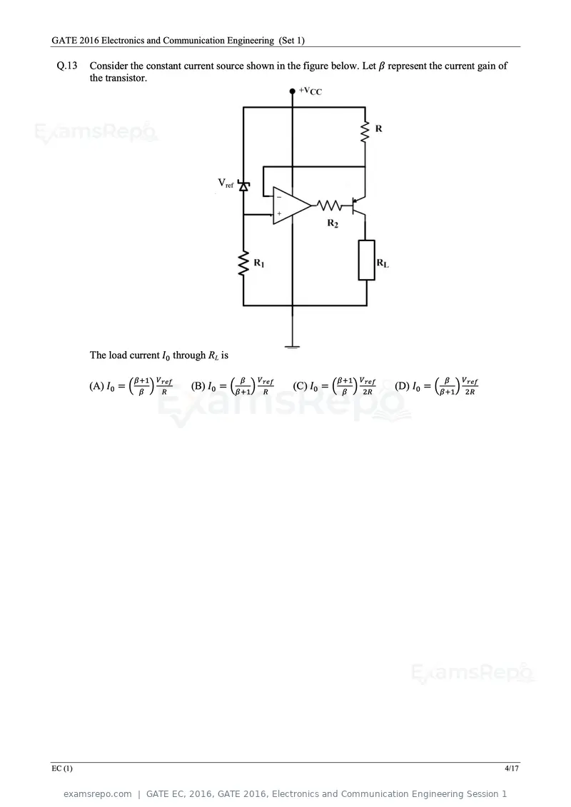
Text of page 6
GATE 2016 Electronics and Communication Engineering (Set 1)

 Q.13    Consider the constant current source shown in the figure below. Let β represent the current gain of
         the transistor.


                                                       ∙
                                       Vref


                                                       ∙
         The load current I0 through RL is

                   β+1 V                      β   V                β+1 V                     β   V
         (A) I0 = � β � ref
                        R
                                 (B) I0 = �β+1� ref
                                                R
                                                                        ref
                                                         (C) I0 = � β � 2R                      ref
                                                                                 (D) I0 = �β+1� 2R


EC (1)                                                                                                     4/17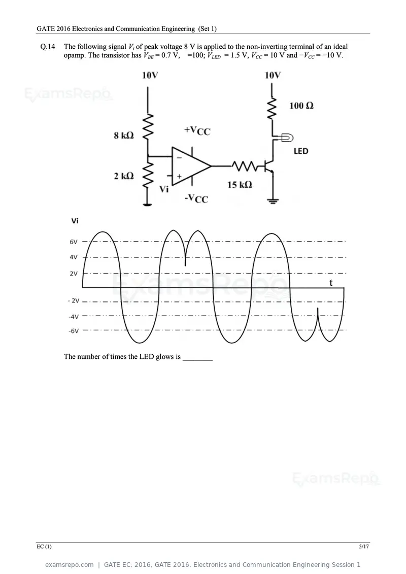
Text of page 7
GATE 2016 Electronics and Communication Engineering (Set 1)

 Q.14    The following signal Vi of peak voltage 8 V is applied to the non-inverting terminal of an ideal
         opamp. The transistor has VBE = 0.7 V, β =100; VLED = 1.5 V, VCC = 10 V and −VCC = −10 V.


                                                                                                  t


         The number of times the LED glows is ________


EC (1)                                                                                                      5/17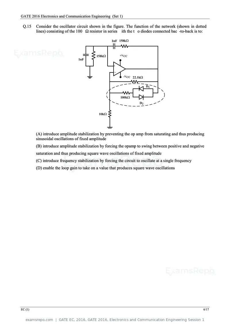
Text of page 8
GATE 2016 Electronics and Communication Engineering (Set 1)

 Q.15    Consider the oscillator circuit shown in the figure. The function of the network (shown in dotted
         lines) consisting of the 100 kΩ resistor in series with the two diodes connected back-to-back is to:


         (A) introduce amplitude stabilization by preventing the op amp from saturating and thus producing
         sinusoidal oscillations of fixed amplitude
         (B) introduce amplitude stabilization by forcing the opamp to swing between positive and negative
         saturation and thus producing square wave oscillations of fixed amplitude
         (C) introduce frequency stabilization by forcing the circuit to oscillate at a single frequency
         (D) enable the loop gain to take on a value that produces square wave oscillations


EC (1)                                                                                                     6/17
Text of page 10
GATE 2016 Electronics and Communication Engineering (Set 1)

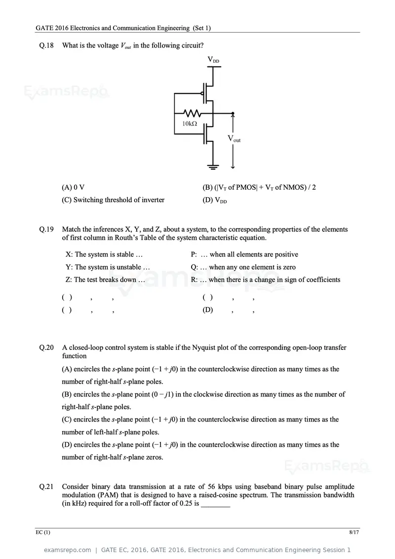
 Q.18    What is the voltage Vout in the following circuit?
                                                              VDD


                                                              ∙

         (A) 0 V                                          (B) (|VT of PMOS| + VT of NMOS) / 2
         (C) Switching threshold of inverter              (D) VDD


 Q.19    Match the inferences X, Y, and Z, about a system, to the corresponding properties of the elements
         of first column in Routh’s Table of the system characteristic equation.

          X: The system is stable …                   P: … when all elements are positive
          Y: The system is unstable …                 Q: … when any one element is zero
          Z: The test breaks down …                   R: … when there is a change in sign of coefficients

         (A) X→P, Y→Q, Z→R                                (B) X→Q, Y→P, Z→R
         (C) X→R, Y→Q, Z→P                                (D) X→P, Y→R, Z→Q


 Q.20    A closed-loop control system is stable if the Nyquist plot of the corresponding open-loop transfer
         function
         (A) encircles the s-plane point (−1 + j0) in the counterclockwise direction as many times as the
         number of right-half s-plane poles.
         (B) encircles the s-plane point (0 − j1) in the clockwise direction as many times as the number of
         right-half s-plane poles.
         (C) encircles the s-plane point (−1 + j0) in the counterclockwise direction as many times as the
         number of left-half s-plane poles.
         (D) encircles the s-plane point (−1 + j0) in the counterclockwise direction as many times as the
         number of right-half s-plane zeros.


 Q.21    Consider binary data transmission at a rate of 56 kbps using baseband binary pulse amplitude
         modulation (PAM) that is designed to have a raised-cosine spectrum. The transmission bandwidth
         (in kHz) required for a roll-off factor of 0.25 is ________


EC (1)                                                                                                        8/17
Text of page 11
GATE 2016 Electronics and Communication Engineering (Set 1)

 Q.22    A superheterodyne receiver operates in the frequency range of 58 MHz − 68 MHz. The
         intermediate frequency fIF and local oscillator frequency fLO are chosen such that fIF ≤ fLO . It is
         required that the image frequencies fall outside the 58 MHz − 68 MHz band. The minimum
         required fIF (in MHz) is ________


 Q.23    The amplitude of a sinusoidal carrier is modulated by a single sinusoid to obtain the amplitude
         modulated signal s(t) = 5 cos 1600πt + 20 cos 1800πt + 5 cos 2000πt. The value of the
         modulation index is __________


 Q.24    Concentric spherical shells of radii 2 m, 4 m, and 8 m carry uniform surface charge densities of
         20 nC/m2, −4 nC/m2 and ρs, respectively. The value of ρs (nC/m2) required to ensure that the
         electric flux density �D⃗ = �0⃗ at radius 10 m is _________


 Q.25    The propagation constant of a lossy transmission line is (2 + j5) m−1 and its characteristic
         impedance is (50 + j0) Ω at ω = 106 rad s−1. The values of the line constants L, C, R, G are,
         respectively,
         (A) L = 200 µH/m, C = 0.1 µF/m, R = 50 Ω/m, G = 0.02 S/m
         (B) L = 250 µH/m, C = 0.1 µF/m, R = 100 Ω/m, G = 0.04 S/m
         (C) L = 200 µH/m, C = 0.2 µF/m, R = 100 Ω/m, G = 0.02 S/m
         (D) L = 250 µH/m, C = 0.2 µF/m, R = 50 Ω/m, G = 0.04 S/m


Q. 26 – Q. 55 carry two marks each.
                       1
 Q.26    The integral 2π ∬D(x + y + 10)dx dy, where D denotes the disc: x 2 + y 2 ≤ 4, evaluates to_____


 Q.27    A sequence x[n] is specified as

               x[n]      1   1n 1
         �           �= �     � � �, for n ≥ 2.
             x[n − 1]    1   0 0

         The initial conditions are x[0] = 1, x[1] = 1, and x[n] = 0 for n < 0. The value of x[12] is ______


 Q.28    In the following integral, the contour C encloses the points 2πj and −2πj
                                                   1         sin z
                                                − �                   dz
                                                  2π C (z − 2πj)3
         The value of the integral is ________


                                                          π        π
 Q.29    The region specified by {( ρ, φ, z): 3 ≤ ρ ≤ 5, 8 ≤ φ ≤ 4 , 3 ≤ z ≤ 4.5} in cylindrical coordinates
         has volume of _______

EC (1)                                                                                                         9/17
Text of page 12
GATE 2016 Electronics and Communication Engineering (Set 1)


 Q.30    The Laplace transform of the causal periodic square wave of period T shown in the figure below is


                            1                                                   1
         (A) F(s) =                                     (B) F(s) =                  sT
                         1+e −sT/2                                             −
                                                                          s�1+e 2 �
                             1                                              1
         (C) F(s) =                                     (D) F(s) =
                       s(1−e −sT )                                        1−e −sT


 Q.31    A network consisting of a finite number of linear resistor (R), inductor (L), and capacitor (C)
         elements, connected all in series or all in parallel, is excited with a source of the form
                                      3

                                     � ak cos(kω0 t) , where ak ≠ 0, ω0 ≠ 0.
                                     k=1

         The source has nonzero impedance. Which one of the following is a possible form of the output
         measured across a resistor in the network?
         (A)                                             (B)
          3                                                     4

         � bk cos(kω0 t + φk ) , where bk ≠ ak , ∀ k           � bk cos(kω0 t + φk ) , where bk ≠ 0, ∀ k
         k=1                                                   k=1
         (C)                                             (D)
                       3                                                    2

                    � ak cos(kω0 t + φk )                                  � ak cos(kω0 t + φk )
                    k=1                                                    k=1


 Q.32    A first-order low-pass filter of time constant T is excited with different input signals (with zero
         initial conditions up to t = 0). Match the excitation signals X, Y, Z with the corresponding time
         responses for t ≥ 0:

          X: Impulse                                          P: 1 − e −t/T
          Y: Unit step                                        Q: t − T(1 − e −t/T )
          Z: Ramp                                             R: e −t/T

         (A) X→R, Y→Q, Z→P                              (B) X→Q, Y→P, Z→R
         (C) X→R, Y→P, Z→Q                              (D) X→P, Y→R, Z→Q


EC (1)                                                                                                     10/17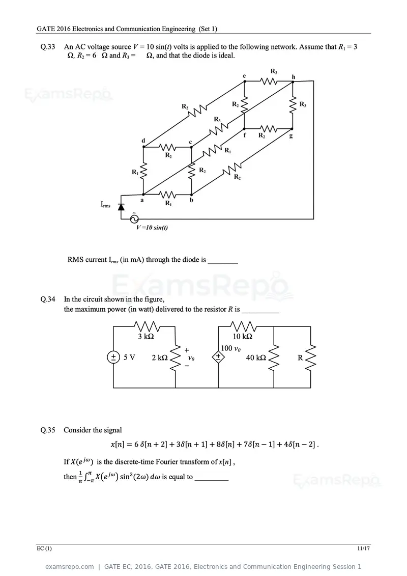
Text of page 13
GATE 2016 Electronics and Communication Engineering (Set 1)

 Q.33    An AC voltage source V = 10 sin(t) volts is applied to the following network. Assume that R1 = 3
         kΩ, R2 = 6 kΩ and R3 = 9 kΩ, and that the diode is ideal.


                      Irms ↑


          RMS current Irms (in mA) through the diode is ________


 Q.34    In the circuit shown in the figure,
         the maximum power (in watt) delivered to the resistor R is __________


                                    3 kΩ                            10 kΩ
                                                               100 v0
                               5V      2 kΩ         v0                  40 kΩ        R


 Q.35    Consider the signal
                          x[n] = 6 δ[n + 2] + 3δ[n + 1] + 8δ[n] + 7δ[n − 1] + 4δ[n − 2] .

         If X(e jω ) is the discrete-time Fourier transform of x[n] ,
              1   π
         then π ∫−π X�e jω � sin2(2ω) dω is equal to _________


EC (1)                                                                                                  11/17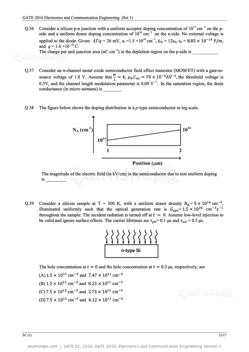
Text of page 14
GATE 2016 Electronics and Communication Engineering (Set 1)

 Q.36    Consider a silicon p-n junction with a uniform acceptor doping concentration of 1017 cm−3 on the p-
         side and a uniform donor doping concentration of 1016 cm−3 on the n-side. No external voltage is
         applied to the diode. Given: kT/q = 26 mV, ni =1.5 ×1010 cm−3, εSi = 12ε0, ε0 = 8.85 × 10⁻¹⁴ F/m,
         and q = 1.6 ×10⁻¹⁹ C.
         The charge per unit junction area (nC cm−2) in the depletion region on the p-side is ___________


 Q.37    Consider an n-channel metal oxide semiconductor field effect transistor (MOSFET) with a gate-to-
                                               W
         source voltage of 1.8 V. Assume that L = 4, μN Cox = 70 × 10−6 AV −2 , the threshold voltage is
         0.3V, and the channel length modulation parameter is 0.09 V−1. In the saturation region, the drain
         conductance (in micro seimens) is ________


 Q.38    The figure below shows the doping distribution in a p-type semiconductor in log scale.


          The magnitude of the electric field (in kV/cm) in the semiconductor due to non uniform doping
          is _________


 Q.39    Consider a silicon sample at T = 300 K, with a uniform donor density Nd = 5 × 1016 cm−3,
         illuminated uniformly such that the optical generation rate is Gopt = 1.5 × 1020 cm−3 s −1
         throughout the sample. The incident radiation is turned off at t = 0. Assume low-level injection to
         be valid and ignore surface effects. The carrier lifetimes are τp0 = 0.1 µs and τn0 = 0.5 µs.


         The hole concentration at t = 0 and the hole concentration at t = 0.3 µs, respectively, are
         (A) 1.5 × 1013 cm−3 and 7.47 × 1011 cm−3
         (B) 1.5 × 1013 cm−3 and 8.23 × 1011 cm−3
         (C) 7.5 × 1013 cm−3 and 3.73 × 1011 cm−3
         (D) 7.5 × 1013 cm−3 and 4.12 × 1011 cm−3


EC (1)                                                                                                    12/17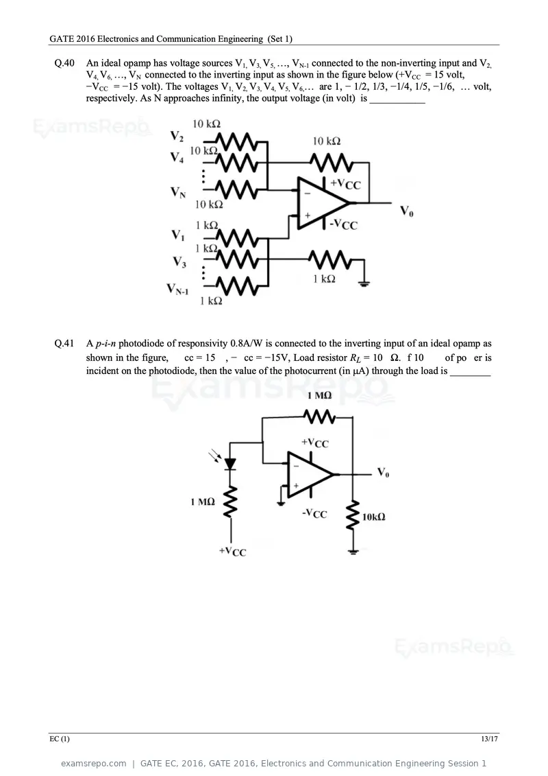
Text of page 15
GATE 2016 Electronics and Communication Engineering (Set 1)

 Q.40    An ideal opamp has voltage sources V1, V3, V5, …, VN-1 connected to the non-inverting input and V2,
         V4, V6, …, VN connected to the inverting input as shown in the figure below (+VCC = 15 volt,
         −VCC = −15 volt). The voltages V1, V2, V3, V4, V5, V6,… are 1, − 1/2, 1/3, −1/4, 1/5, −1/6, … volt,
         respectively. As N approaches infinity, the output voltage (in volt) is ___________


 Q.41    A p-i-n photodiode of responsivity 0.8A/W is connected to the inverting input of an ideal opamp as
         shown in the figure, +Vcc = 15 V, −Vcc = −15V, Load resistor RL = 10 kΩ. If 10 µW of power is
         incident on the photodiode, then the value of the photocurrent (in µA) through the load is ________


EC (1)                                                                                                   13/17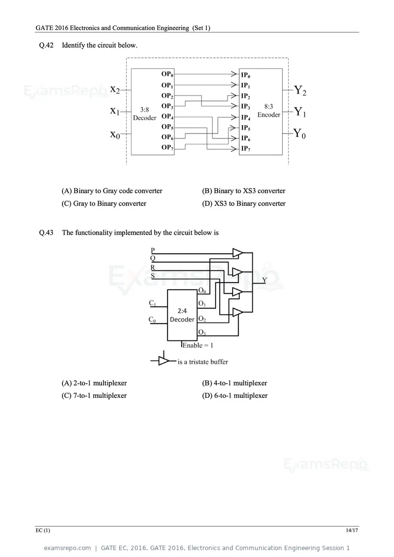
Text of page 16
GATE 2016 Electronics and Communication Engineering (Set 1)

 Q.42    Identify the circuit below.


         (A) Binary to Gray code converter              (B) Binary to XS3 converter
         (C) Gray to Binary converter                   (D) XS3 to Binary converter


 Q.43    The functionality implemented by the circuit below is


         (A) 2-to-1 multiplexer                         (B) 4-to-1 multiplexer
         (C) 7-to-1 multiplexer                         (D) 6-to-1 multiplexer


EC (1)                                                                                14/17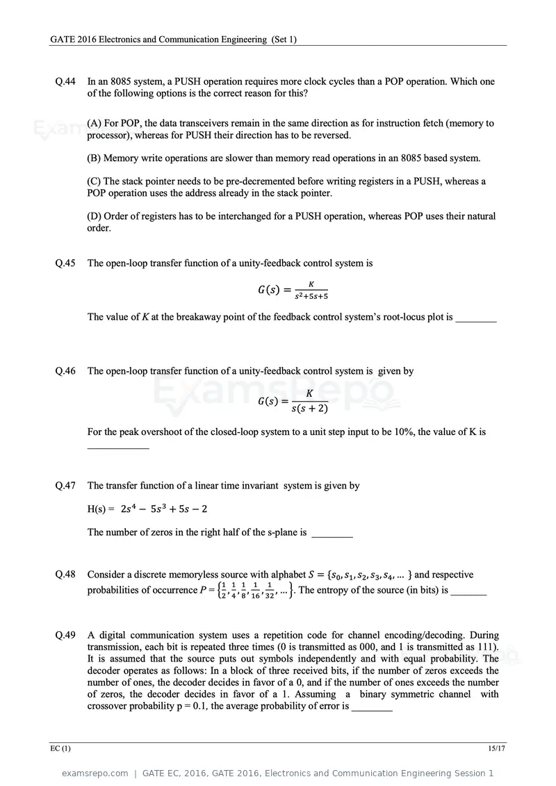
Text of page 17
GATE 2016 Electronics and Communication Engineering (Set 1)


 Q.44    In an 8085 system, a PUSH operation requires more clock cycles than a POP operation. Which one
         of the following options is the correct reason for this?

         (A) For POP, the data transceivers remain in the same direction as for instruction fetch (memory to
         processor), whereas for PUSH their direction has to be reversed.

         (B) Memory write operations are slower than memory read operations in an 8085 based system.

         (C) The stack pointer needs to be pre-decremented before writing registers in a PUSH, whereas a
         POP operation uses the address already in the stack pointer.

         (D) Order of registers has to be interchanged for a PUSH operation, whereas POP uses their natural
         order.


 Q.45    The open-loop transfer function of a unity-feedback control system is
                                                                   K
                                                      G(s) = s2 +5s+5

         The value of K at the breakaway point of the feedback control system’s root-locus plot is ________


 Q.46    The open-loop transfer function of a unity-feedback control system is given by

                                                                  K
                                                      G(s) =
                                                               s(s + 2)

         For the peak overshoot of the closed-loop system to a unit step input to be 10%, the value of K is
         ____________


 Q.47    The transfer function of a linear time invariant system is given by

         H(s) = 2s 4 − 5s 3 + 5s − 2

         The number of zeros in the right half of the s-plane is ________


 Q.48    Consider a discrete memoryless source with alphabet S = {s0 , s1 , s2 , s3 , s4 , … } and respective
                                          1 1 1 1 1
         probabilities of occurrence P = �2 , 4 , 8 , 16 , 32 , … �. The entropy of the source (in bits) is _______


 Q.49    A digital communication system uses a repetition code for channel encoding/decoding. During
         transmission, each bit is repeated three times (0 is transmitted as 000, and 1 is transmitted as 111).
         It is assumed that the source puts out symbols independently and with equal probability. The
         decoder operates as follows: In a block of three received bits, if the number of zeros exceeds the
         number of ones, the decoder decides in favor of a 0, and if the number of ones exceeds the number
         of zeros, the decoder decides in favor of a 1. Assuming a binary symmetric channel with
         crossover probability p = 0.1, the average probability of error is ________


EC (1)                                                                                                                15/17
Text of page 18
GATE 2016 Electronics and Communication Engineering (Set 1)


 Q.50    An analog pulse s(t) is transmitted over an additive white Gaussian noise (AWGN) channel. The
         received signal is r(t) = s(t) + n(t), where n(t) is additive white Gaussian noise with power spectral
                 N
         density 0 . The received signal is passed through a filter with impulse response h(t). Let Es and Eℎ
                 2
         denote the energies of the pulse s(t) and the filter h(t), respectively. When the signal-to-noise ratio
         (SNR) is maximized at the output of the filter (SNRmax), which of the following holds?
                                   2E                                                E
         (A) Es = Eℎ ; SNR max = N s                       (B) Es = Eℎ ; SNR max = 2Ns
                                     0                                                   0
                                 2E                                                2E
         (C) Es > Eℎ ; SNR max > N s                       (D) Es < Eℎ ; SNR max = N ℎ
                                  0                                                  0


 Q.51    The current density in a medium is given by
                                                       400 sinθ
                                              �J⃗ =               a� Am−2
                                                      2π(r 2 + 4) r
         The total current and the average current density flowing through the portion of a spherical surface
                     π         π
         r = 0.8 m,
                    12
                        ≤ θ ≤ , 0 ≤ φ ≤ 2π are given, respectively, by
                               4

         (A) 15.09 A, 12.86 Am-2                           (B) 18.73 A, 13.65 Am-2
         (C) 12.86 A, 9.23 Am-2                            (D) 10.28 A, 7.56 Am-2


 Q.52    An antenna pointing in a certain direction has a noise temperature of 50 K. The ambient
         temperature is 290 K. The antenna is connected to a pre-amplifier that has a noise figure of 2 dB
         and an available gain of 40 dB over an effective bandwidth of 12 MHz. The effective input noise
         temperature Te for the amplifier and the noise power Pao at the output of the preamplifier,
         respectively, are
         (A) Te = 169.36 K and Pao = 3.73×10⁻¹⁰ W          (B) Te = 170.8 K and Pao = 4.56×10⁻¹⁰ W
         (C) Te = 182.5 K and Pao = 3.85×10⁻¹⁰ W           (D) Te = 160.62 K and Pao = 4.6×10⁻¹⁰ W


 Q.53    Two lossless X-band horn antennas are separated by a distance of 200λ. The amplitude reflection
         coefficients at the terminals of the transmitting and receiving antennas are 0.15 and 0.18,
         respectively. The maximum directivities of the transmitting and receiving antennas (over the
         isotropic antenna) are 18 dB and 22 dB, respectively. Assuming that the input power in the lossless
         transmission line connected to the antenna is 2 W, and that the antennas are perfectly aligned and
         polarization matched, the power ( in mW) delivered to the load at the receiver is ________


EC (1)                                                                                                       16/17
Text of page 19
GATE 2016 Electronics and Communication Engineering (Set 1)


 Q.54    The electric field of a uniform plane wave travelling along the negative z direction is given by the
         following equation:
                                               E�⃗wi = �a�x + ja�y �E0 e jkz

         This wave is incident upon a receiving antenna placed at the origin and whose radiated electric field
         towards the incident wave is given by the following equation:

                                                                   1
                                             E�⃗a = �a�x + 2a�y �EI e −jkr
                                                                   r

         The polarization of the incident wave, the polarization of the antenna and losses due to the
         polarization mismatch are, respectively,
         (A) Linear, Circular (clockwise), −5dB           (B) Circular (clockwise), Linear, −5dB
         (C) Circular (clockwise), Linear, −3dB           (D) Circular (anti clockwise), Linear, −3dB


 Q.55    The far-zone power density radiated by a helical antenna is approximated as:
                                                                    1
                                       W���⃗rad = W
                                                  ���⃗average ≈ ar
                                                                �C0 2 cos 4 θ
                                                                    r
         The radiated power density is symmetrical with respect to φ and exists only in the upper
                              π
         hemisphere: 0 ≤ θ ≤ ; 0 ≤ φ ≤ 2π; C0 is a constant. The power radiated by the antenna (in
                              2
         watts) and the maximum directivity of the antenna, respectively, are
         (A) 1.5C0 , 10dB        (B) 1.256C0 , 10dB       (C) 1.256C0 , 12dB       (D) 1.5C0 , 12dB


                               END OF THE QUESTION PAPER


EC (1)                                                                                                      17/17
Text of page 20
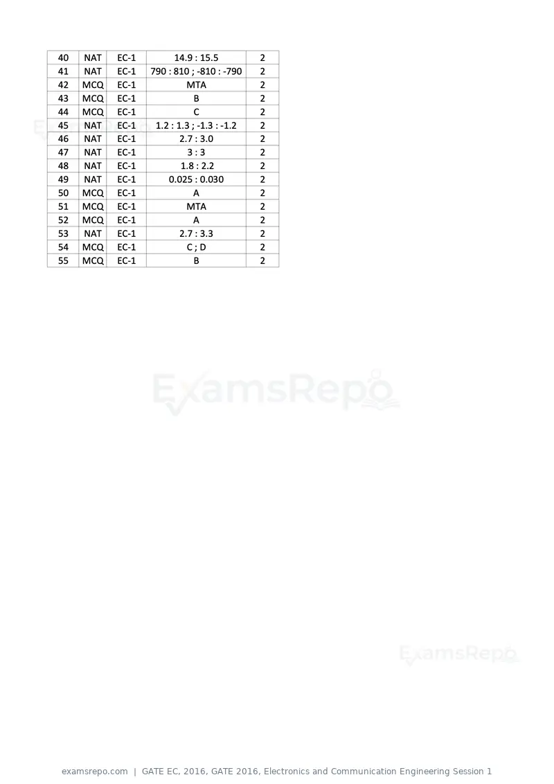
Q. No Type Section        Key        Marks
  1   MCQ    GA            A          1
  2   MCQ    GA            B          1
  3   MCQ    GA            A          1
  4   MCQ    GA            A          1
  5   MCQ    GA            C          1
  6   MCQ    GA            C          2
  7   MCQ    GA            B          2
  8   MCQ    GA            D          2
  9   MCQ    GA            C          2
 10 MCQ      GA            C          2
  1   MCQ EC-1             C          1
  2   NAT   EC-1        0.9 : 1.1     1
  3   MCQ EC-1             B          1
  4   MCQ EC-1             A          1
  5   MCQ EC-1             C          1
  6   MCQ EC-1             C          1
  7   MCQ EC-1             B          1
  8   MCQ EC-1             B          1
  9   MCQ EC-1             D          1
 10   NAT   EC-1         12 : 14      1
 11 MCQ EC-1               A          1
 12 MCQ EC-1               C          1
 13 MCQ EC-1               B          1
 14   NAT   EC-1        2.9 : 3.1     1
 15 MCQ EC-1               A          1
 16 MCQ EC-1               A          1
 17 MCQ EC-1               C          1
 18 MCQ EC-1               C          1
 19 MCQ EC-1               D          1
 20 MCQ EC-1               A          1
 21   NAT   EC-1      34.5 : 35.5     1
 22   NAT   EC-1        4.9 : 5.1     1
 23   NAT   EC-1      0.49 : 0.51     1
 24   NAT   EC-1     -0.28 : -0.22    1
 25 MCQ EC-1               B          1
 26   NAT   EC-1         18 : 22      2
 27   NAT   EC-1       230 : 240      2
 28   NAT   EC-1      -136 : -132     2
 29   NAT   EC-1      4.66 : 4.76     2
 30 MCQ EC-1              MTA         2
 31 MCQ EC-1               A          2
 32 MCQ EC-1               C          2
 33   NAT   EC-1        0.9 : 1.1     2
 34   NAT   EC-1      0.78 : 0.82     2
 35   NAT   EC-1        7.9 : 8.1     2
 36   NAT   EC-1       -5.0 : -4.6    2
 37   NAT   EC-1         28 : 29      2
 38   NAT   EC-1      1.10 : 1.25     2
 39 MCQ EC-1               A          2
Text of page 21
40   NAT   EC-1         14.9 : 15.5          2
41   NAT   EC-1   790 : 810 ; -810 : -790    2
42   MCQ   EC-1             MTA              2
43   MCQ   EC-1               B              2
44   MCQ   EC-1               C              2
45   NAT   EC-1    1.2 : 1.3 ; -1.3 : -1.2   2
46   NAT   EC-1           2.7 : 3.0          2
47   NAT   EC-1             3:3              2
48   NAT   EC-1           1.8 : 2.2          2
49   NAT   EC-1       0.025 : 0.030          2
50   MCQ   EC-1               A              2
51   MCQ   EC-1             MTA              2
52   MCQ   EC-1               A              2
53   NAT   EC-1           2.7 : 3.3          2
54   MCQ   EC-1             C;D              2
55   MCQ   EC-1               B              2

Text of page 22
GATE 2016                                                                    General Aptitude - GA Set-3


Q. 1 – Q. 5 carry one mark each.
Q.1    Based on the given statements, select the appropriate option with respect to grammar and usage.

       Statements
           (i)    The height of Mr. X is 6 feet.
           (ii)   The height of Mr. Y is 5 feet.

      (A) Mr. X is longer than Mr. Y.

      (B) Mr. X is more elongated than Mr. Y.

      (C) Mr. X is taller than Mr. Y.

      (D) Mr. X is lengthier than Mr. Y.


Q.2    The students ___________ the teacher on teachers’ day for twenty years of dedicated teaching.

      (A) facilitated          (B) felicitated         (C) fantasized          (D) facillitated


Q.3    After India’s cricket world cup victory in 1985, Shrotria who was playing both tennis and cricket
       till then, decided to concentrate only on cricket. And the rest is history.

       What does the underlined phrase mean in this context?
      (A) history will rest in peace                   (B) rest is recorded in history books

      (C) rest is well known                           (D) rest is archaic


Q.4                    ½              ½
       Given (9 inches) = (0.25 yards) , which one of the following statements is TRUE?


      (A) 3 inches = 0.5 yards                         (B) 9 inches = 1.5 yards

      (C) 9 inches = 0.25 yards                        (D) 81 inches = 0.0625 yards


Q.5    S, M, E and F are working in shifts in a team to finish a project. M works with twice the efficiency
       of others but for half as many days as E worked. S and M have 6 hour shifts in a day, whereas E
       and F have 12 hours shifts. What is the ratio of contribution of M to contribution of E in the
       project?

       (A) 1:1                   (B) 1:2                  (C) 1:4                  (D) 2:1


                                                                                                              1/3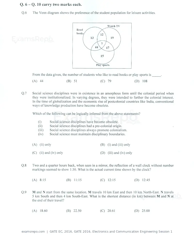
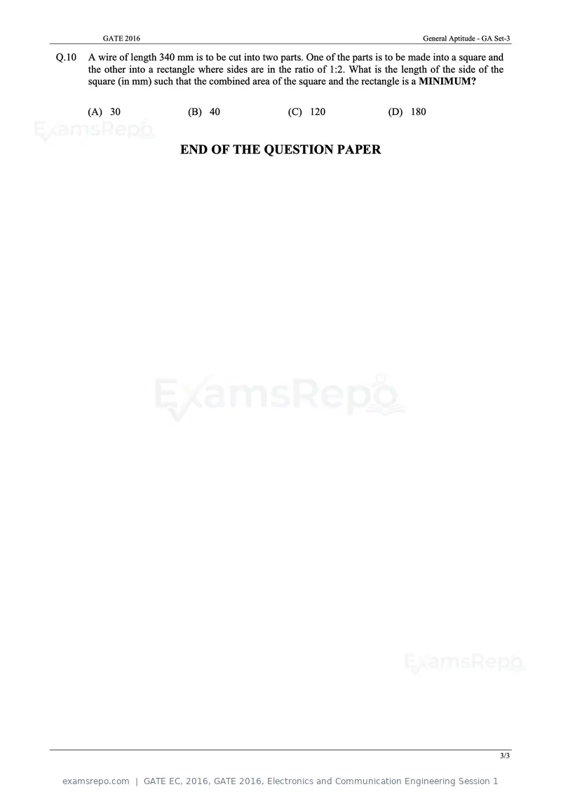
Text of page 24
GATE 2016                                                                     General Aptitude - GA Set-3

Q.10   A wire of length 340 mm is to be cut into two parts. One of the parts is to be made into a square and
       the other into a rectangle where sides are in the ratio of 1:2. What is the length of the side of the
       square (in mm) such that the combined area of the square and the rectangle is a MINIMUM?

       (A) 30                  (B) 40                  (C) 120                 (D) 180


                             END OF THE QUESTION PAPER


                                                                                                               3/3
Text of page 25
GATE 2016 Electronics and Communication Engineering (Set 2)

Q. 1 – Q. 25 carry one mark each.
 Q.1
                                                   3  2   4
         The value of x for which the matrix A = � 9  7  13 �
                                                  −6 −4 −9 + x
         has zero as an eigenvalue is ________


 Q.2     Consider the complex valued function f(z) = 2z 3 + b |z|3 where z is a complex variable.
         The value of b for which the function f(z) is analytic is ________


 Q.3     As x varies from −1 to +3, which one of the following describes the behaviour of the function
         f(x) = x 3 – 3x 2 + 1?
         (A) f(x) increases monotonically.
         (B) f(x) increases, then decreases and increases again.
         (C) f(x) decreases, then increases and decreases again.
         (D) f(x) increases and then decreases.


 Q.4     How many distinct values of x satisfy the equation sin(x) = x/2, where x is in radians?
         (A) 1                   (B) 2                    (C) 3                    (D) 4 or more


 Q.5     Consider the time-varying vector I = x� 15 cos(ωt) + y� 5 sin(ωt) in Cartesian coordinates, where
         ω > 0 is a constant. When the vector magnitude |I| is at its minimum value, the angle θ that I
         makes with the x axis (in degrees, such that 0 ≤ θ ≤ 180) is ________


 Q.6     In the circuit shown below, VS is a constant voltage source and IL is a constant current load.


         The value of IL that maximizes the power absorbed by the constant current load is
               VS                      VS                       VS                 (D) ∞
         (A)                     (B)                      (C)
               4R                      2R                       R


EC (2)                                                                                                    1/14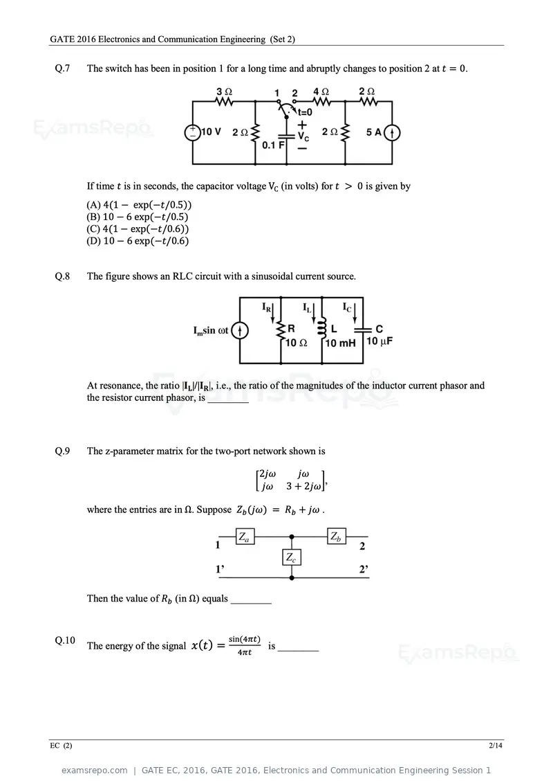
Text of page 26
GATE 2016 Electronics and Communication Engineering (Set 2)


 Q.7     The switch has been in position 1 for a long time and abruptly changes to position 2 at t = 0.


         If time t is in seconds, the capacitor voltage VC (in volts) for t > 0 is given by
         (A) 4(1 − exp(−t/0.5))
         (B) 10 − 6 exp(−t/0.5)
         (C) 4(1 − exp(−t/0.6))
         (D) 10 − 6 exp(−t/0.6)


 Q.8     The figure shows an RLC circuit with a sinusoidal current source.


         At resonance, the ratio |IL |/|IR |, i.e., the ratio of the magnitudes of the inductor current phasor and
         the resistor current phasor, is ________


 Q.9     The z-parameter matrix for the two-port network shown is

                                                          2jω     jω
                                                      �                 �,
                                                          jω    3 + 2jω

         where the entries are in Ω. Suppose Zb (jω) = Rb + jω .


         Then the value of Rb (in Ω) equals ________


 Q.10                                         sin(4πt)
         The energy of the signal x (t ) =                 is ________
                                                4πt


EC (2)                                                                                                               2/14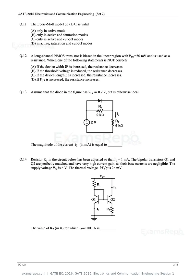
Text of page 27
GATE 2016 Electronics and Communication Engineering (Set 2)


 Q.11    The Ebers-Moll model of a BJT is valid
         (A) only in active mode
         (B) only in active and saturation modes
         (C) only in active and cut-off modes
         (D) in active, saturation and cut-off modes


 Q.12    A long-channel NMOS transistor is biased in the linear region with VDS =50 mV and is used as a
         resistance. Which one of the following statements is NOT correct?
         (A) If the device width W is increased, the resistance decreases.
         (B) If the threshold voltage is reduced, the resistance decreases.
         (C) If the device length L is increased, the resistance increases.
         (D) If VGS is increased, the resistance increases.


 Q.13    Assume that the diode in the figure has Von = 0.7 V, but is otherwise ideal.


         The magnitude of the current i2 (in mA) is equal to ________


 Q.14    Resistor R1 in the circuit below has been adjusted so that I1 = 1 mA. The bipolar transistors Q1 and
         Q2 are perfectly matched and have very high current gain, so their base currents are negligible. The
         supply voltage Vcc is 6 V. The thermal voltage kT/q is 26 mV.


         The value of R 2 (in Ω) for which I2 =100 µA is ________


EC (2)                                                                                                     3/14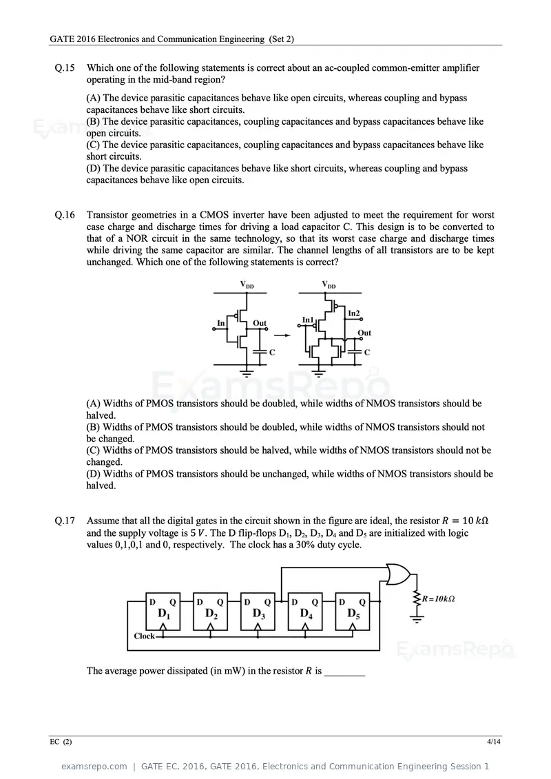
Text of page 28
GATE 2016 Electronics and Communication Engineering (Set 2)


 Q.15    Which one of the following statements is correct about an ac-coupled common-emitter amplifier
         operating in the mid-band region?
         (A) The device parasitic capacitances behave like open circuits, whereas coupling and bypass
         capacitances behave like short circuits.
         (B) The device parasitic capacitances, coupling capacitances and bypass capacitances behave like
         open circuits.
         (C) The device parasitic capacitances, coupling capacitances and bypass capacitances behave like
         short circuits.
         (D) The device parasitic capacitances behave like short circuits, whereas coupling and bypass
         capacitances behave like open circuits.


 Q.16    Transistor geometries in a CMOS inverter have been adjusted to meet the requirement for worst
         case charge and discharge times for driving a load capacitor C. This design is to be converted to
         that of a NOR circuit in the same technology, so that its worst case charge and discharge times
         while driving the same capacitor are similar. The channel lengths of all transistors are to be kept
         unchanged. Which one of the following statements is correct?


         (A) Widths of PMOS transistors should be doubled, while widths of NMOS transistors should be
         halved.
         (B) Widths of PMOS transistors should be doubled, while widths of NMOS transistors should not
         be changed.
         (C) Widths of PMOS transistors should be halved, while widths of NMOS transistors should not be
         changed.
         (D) Widths of PMOS transistors should be unchanged, while widths of NMOS transistors should be
         halved.


 Q.17    Assume that all the digital gates in the circuit shown in the figure are ideal, the resistor R = 10 kΩ
         and the supply voltage is 5 V. The D flip-flops D1, D2, D3, D4 and D5 are initialized with logic
         values 0,1,0,1 and 0, respectively. The clock has a 30% duty cycle.


         The average power dissipated (in mW) in the resistor R is ________


EC (2)                                                                                                        4/14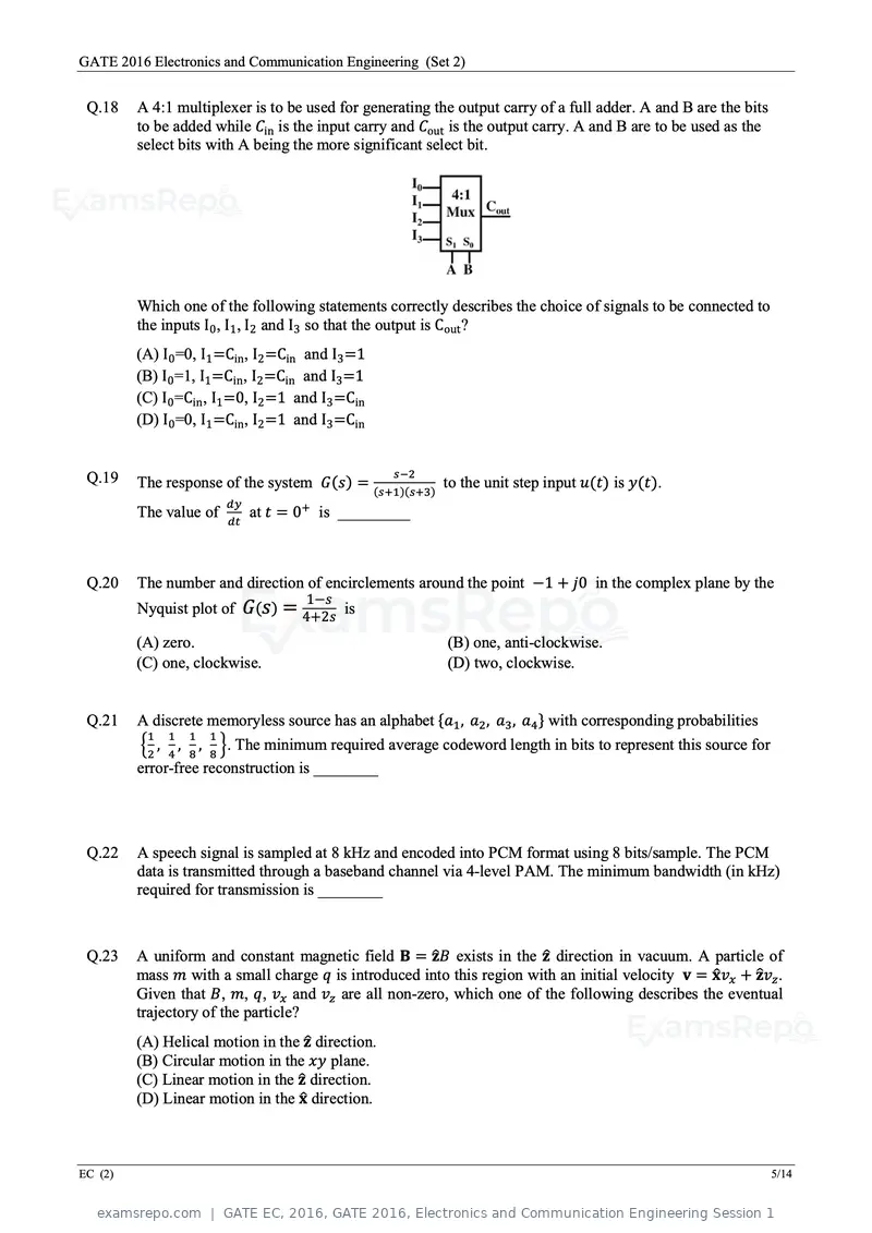
Text of page 29
GATE 2016 Electronics and Communication Engineering (Set 2)


 Q.18    A 4:1 multiplexer is to be used for generating the output carry of a full adder. A and B are the bits
         to be added while Cin is the input carry and Cout is the output carry. A and B are to be used as the
         select bits with A being the more significant select bit.


         Which one of the following statements correctly describes the choice of signals to be connected to
         the inputs I0 , I1 , I2 and I3 so that the output is Cout ?
         (A) I0 =0, I1 =Cin, I2 =Cin and I3 =1
         (B) I0 =1, I1 =Cin, I2 =Cin and I3 =1
         (C) I0 =Cin, I1 =0, I2 =1 and I3 =Cin
         (D) I0 =0, I1 =Cin, I2 =1 and I3 =Cin


 Q.19                                              s−2
         The response of the system G(s) = (s+1)(s+3) to the unit step input u(t) is y(t).
                       dy
         The value of dt at t = 0+ is _________


 Q.20    The number and direction of encirclements around the point −1 + j0 in the complex plane by the
                                    1−s
         Nyquist plot of G(s) = 4+2s is

         (A) zero.                                        (B) one, anti-clockwise.
         (C) one, clockwise.                              (D) two, clockwise.


 Q.21    A discrete memoryless source has an alphabet {a1 , a2 , a3 , a4 } with corresponding probabilities
           1 1 1 1
         �2 , 4 , 8 , 8 �. The minimum required average codeword length in bits to represent this source for
         error-free reconstruction is ________


 Q.22    A speech signal is sampled at 8 kHz and encoded into PCM format using 8 bits/sample. The PCM
         data is transmitted through a baseband channel via 4-level PAM. The minimum bandwidth (in kHz)
         required for transmission is ________


 Q.23    A uniform and constant magnetic field B = z�B exists in the z� direction in vacuum. A particle of
         mass m with a small charge q is introduced into this region with an initial velocity v = x�vx + z�vz .
         Given that B, m, q, vx and vz are all non-zero, which one of the following describes the eventual
         trajectory of the particle?
         (A) Helical motion in the z� direction.
         (B) Circular motion in the xy plane.
         (C) Linear motion in the z� direction.
         (D) Linear motion in the x� direction.


EC (2)                                                                                                           5/14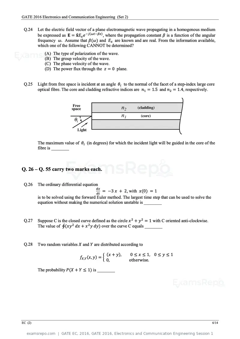
Text of page 30
GATE 2016 Electronics and Communication Engineering (Set 2)


 Q.24    Let the electric field vector of a plane electromagnetic wave propagating in a homogenous medium
         be expressed as E = x�Ex e −j(ωt−βz) , where the propagation constant β is a function of the angular
         frequency ω. Assume that β(ω) and Ex are known and are real. From the information available,
         which one of the following CANNOT be determined?
             (A) The type of polarization of the wave.
             (B) The group velocity of the wave.
             (C) The phase velocity of the wave.
             (D) The power flux through the z = 0 plane.


 Q.25    Light from free space is incident at an angle θi to the normal of the facet of a step-index large core
         optical fibre. The core and cladding refractive indices are n1 = 1.5 and n2 = 1.4, respectively.


         The maximum value of θi (in degrees) for which the incident light will be guided in the core of the
         fibre is ________


Q. 26 – Q. 55 carry two marks each.

 Q.26    The ordinary differential equation
                                          dx
                                          dt
                                             = −3 x + 2, with x(0) = 1
         is to be solved using the forward Euler method. The largest time step that can be used to solve the
         equation without making the numerical solution unstable is ________


 Q.27    Suppose C is the closed curve defined as the circle x 2 + y 2 = 1 with C oriented anti-clockwise.
         The value of ∮(xy 2 dx + x 2 y dy) over the curve C equals ________


 Q.28    Two random variables X and Y are distributed according to

                                                   (x + y),    0 ≤ x ≤ 1, 0 ≤ y ≤ 1
                                 fX,Y (x, y) = �
                                                   0,         otherwise.

         The probability P(X + Y ≤ 1) is ________


EC (2)                                                                                                         6/14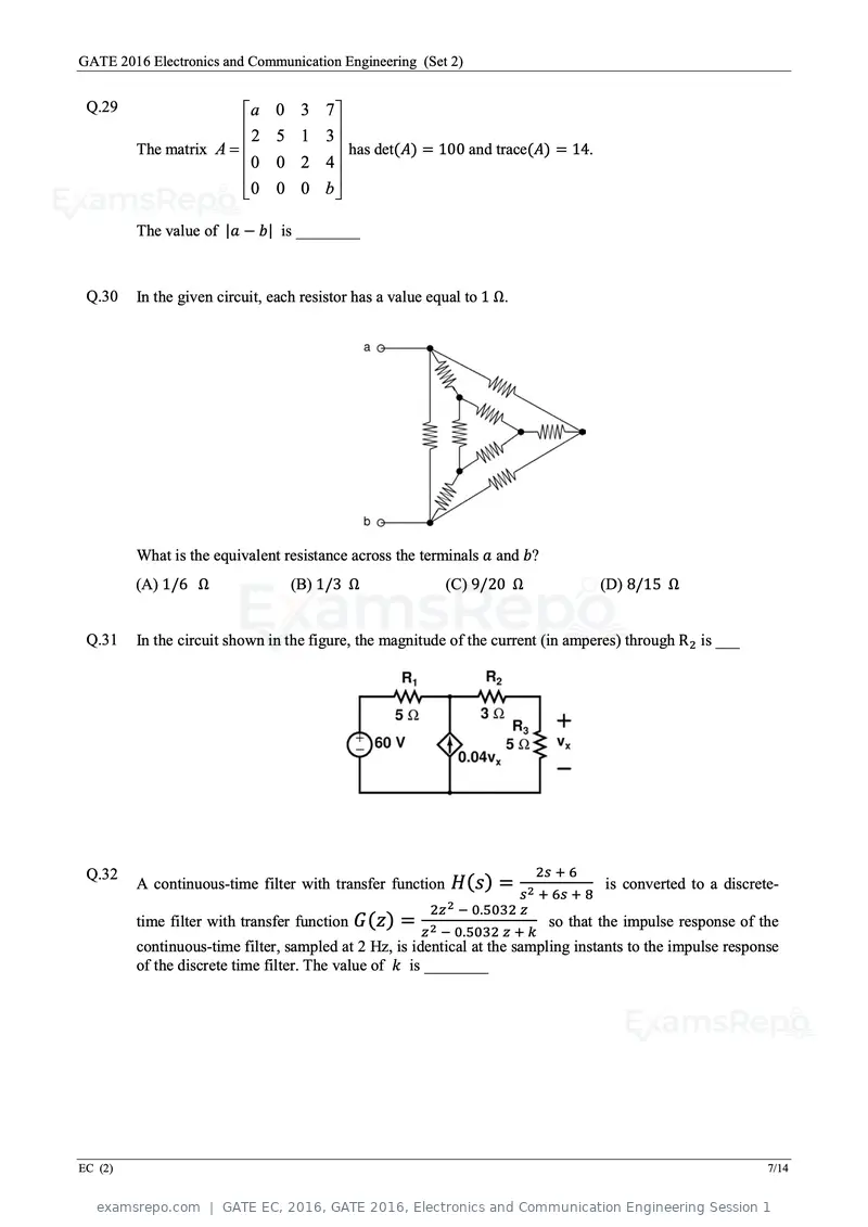
Text of page 31
GATE 2016 Electronics and Communication Engineering (Set 2)
Q.29 a 0 3 7
2 5 1 3
The matrix A = has det(A) = 100 and trace(A) = 14.
0 0 2 4
0 0 0 b
The value of |a − b| is ________
Q.30 In the given circuit, each resistor has a value equal to 1 Ω.
What is the equivalent resistance across the terminals a and b?
(A) 1/6 Ω (B) 1/3 Ω (C) 9/20 Ω (D) 8/15 Ω
Q.31 In the circuit shown in the figure, the magnitude of the current (in amperes) through R 2 is ___
Q.32 2s + 6
A continuous-time filter with transfer function H(s) = is converted to a discrete-
s 2 + 6s + 8
2z 2 − 0.5032 z
time filter with transfer function G(z) = so that the impulse response of the
z 2 − 0.5032 z + k
continuous-time filter, sampled at 2 Hz, is identical at the sampling instants to the impulse response
of the discrete time filter. The value of k is ________
EC (2) 7/14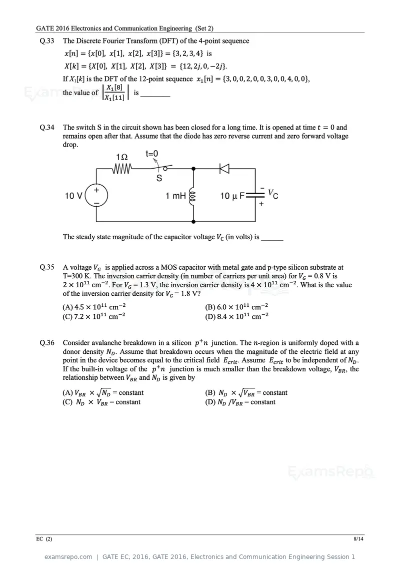
Text of page 32
GATE 2016 Electronics and Communication Engineering (Set 2)
 Q.33    The Discrete Fourier Transform (DFT) of the 4-point sequence
         x[n] = {x[0], x[1], x[2], x[3]} = {3, 2, 3, 4} is
         X[k] = {X[0], X[1], X[2], X[3]} = {12, 2j, 0, −2j}.
         If X1[k] is the DFT of the 12-point sequence x1 [n] = {3, 0, 0, 2, 0, 0, 3, 0, 0, 4, 0, 0},
                          X1 [8]
         the value of �           � is ________
                          X1 [11]


 Q.34    The switch S in the circuit shown has been closed for a long time. It is opened at time t = 0 and
         remains open after that. Assume that the diode has zero reverse current and zero forward voltage
         drop.


         The steady state magnitude of the capacitor voltage VC (in volts) is ______


 Q.35    A voltage VG is applied across a MOS capacitor with metal gate and p-type silicon substrate at
         T=300 K. The inversion carrier density (in number of carriers per unit area) for VG = 0.8 V is
         2 × 1011 cm−2. For VG = 1.3 V, the inversion carrier density is 4 × 1011 cm−2 . What is the value
         of the inversion carrier density for VG = 1.8 V?
         (A) 4.5 × 1011 cm−2                                 (B) 6.0 × 1011 cm−2
         (C) 7.2 × 1011 cm−2                                 (D) 8.4 × 1011 cm−2


 Q.36    Consider avalanche breakdown in a silicon p+ n junction. The n-region is uniformly doped with a
         donor density ND . Assume that breakdown occurs when the magnitude of the electric field at any
         point in the device becomes equal to the critical field Ecrit . Assume Ecrit to be independent of ND .
         If the built-in voltage of the p+ n junction is much smaller than the breakdown voltage, VBR , the
         relationship between VBR and ND is given by

         (A) VBR × �ND = constant                            (B) ND × �VBR = constant
         (C) ND × VBR = constant                             (D) ND /VBR = constant


EC (2)                                                                                                       8/14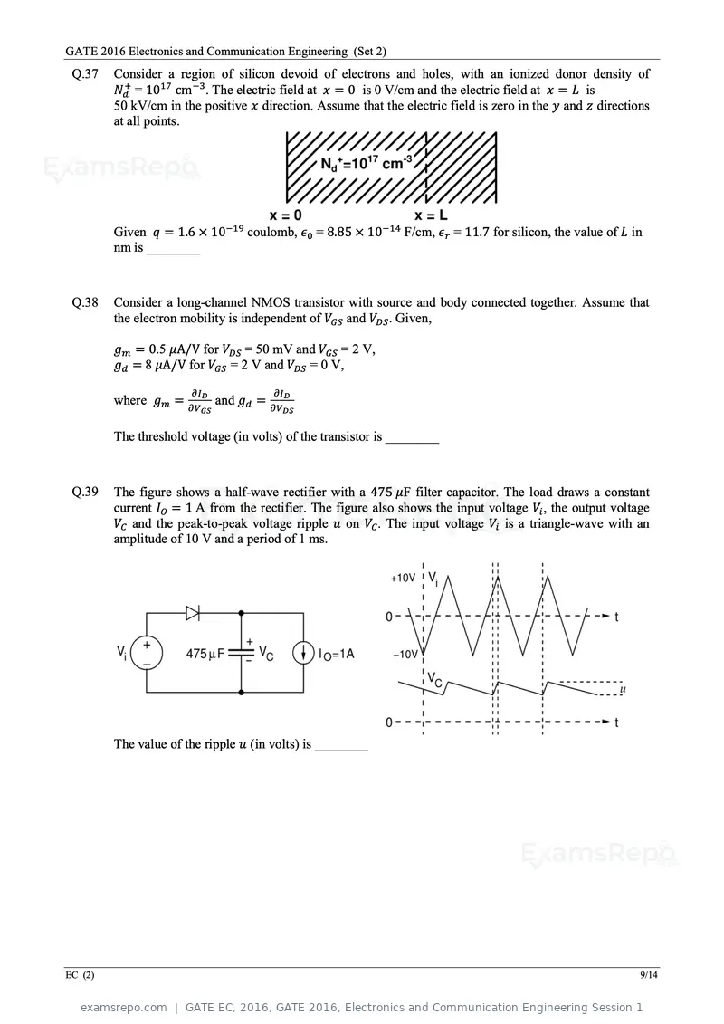
Text of page 33
GATE 2016 Electronics and Communication Engineering (Set 2)
 Q.37    Consider a region of silicon devoid of electrons and holes, with an ionized donor density of
         Nd+ = 1017 cm−3 . The electric field at x = 0 is 0 V/cm and the electric field at x = L is
         50 kV/cm in the positive x direction. Assume that the electric field is zero in the y and z directions
         at all points.


         Given q = 1.6 × 10⁻¹⁹ coulomb, ε0 = 8.85 × 10⁻¹⁴ F/cm, εr = 11.7 for silicon, the value of L in
         nm is ________


 Q.38    Consider a long-channel NMOS transistor with source and body connected together. Assume that
         the electron mobility is independent of VGS and VDS . Given,

         gm = 0.5 μA/V for VDS = 50 mV and VGS = 2 V,
         gd = 8 μA/V for VGS = 2 V and VDS = 0 V,

                       ∂I              ∂I
         where gm = ∂V D and gd = ∂V D
                         GS              DS


         The threshold voltage (in volts) of the transistor is ________


 Q.39    The figure shows a half-wave rectifier with a 475 μF filter capacitor. The load draws a constant
         current IO = 1 A from the rectifier. The figure also shows the input voltage Vi , the output voltage
         VC and the peak-to-peak voltage ripple u on VC . The input voltage Vi is a triangle-wave with an
         amplitude of 10 V and a period of 1 ms.


         The value of the ripple u (in volts) is ________


EC (2)                                                                                                       9/14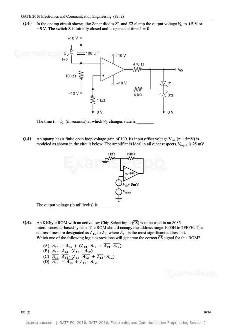
Text of page 34
GATE 2016 Electronics and Communication Engineering (Set 2)
 Q.40    In the opamp circuit shown, the Zener diodes Z1 and Z2 clamp the output voltage VO to +5 V or
         −5 V. The switch S is initially closed and is opened at time t = 0.


         The time t = t1 (in seconds) at which VO changes state is ________


 Q.41    An opamp has a finite open loop voltage gain of 100. Its input offset voltage Vios (= +5mV) is
         modeled as shown in the circuit below. The amplifier is ideal in all other respects. Vinput is 25 mV.


         The output voltage (in millivolts) is ________


 Q.42    An 8 Kbyte ROM with an active low Chip Select input (CS   ���) is to be used in an 8085
         microprocessor based system. The ROM should occupy the address range 1000H to 2FFFH. The
         address lines are designated as A15 to A0 , where A15 is the most significant address bit.
         Which one of the following logic expressions will generate the correct ���CS signal for this ROM?
             (A) A15 + A14 + (A13 ⋅ A12 + A      �����  �����
                                                   13 ⋅ A12 )
             (B) A15 ⋅ A14 ⋅ (A13 + A12 )
                 �����
             (C) A      �����        ����� �����
                   15 ⋅ A14 ⋅ (A13 ⋅ A12 + A13 ⋅ A12 )
                 �����
             (D) A          �����
                   15 + A14 + A13 ⋅ A12


EC (2)                                                                                                       10/14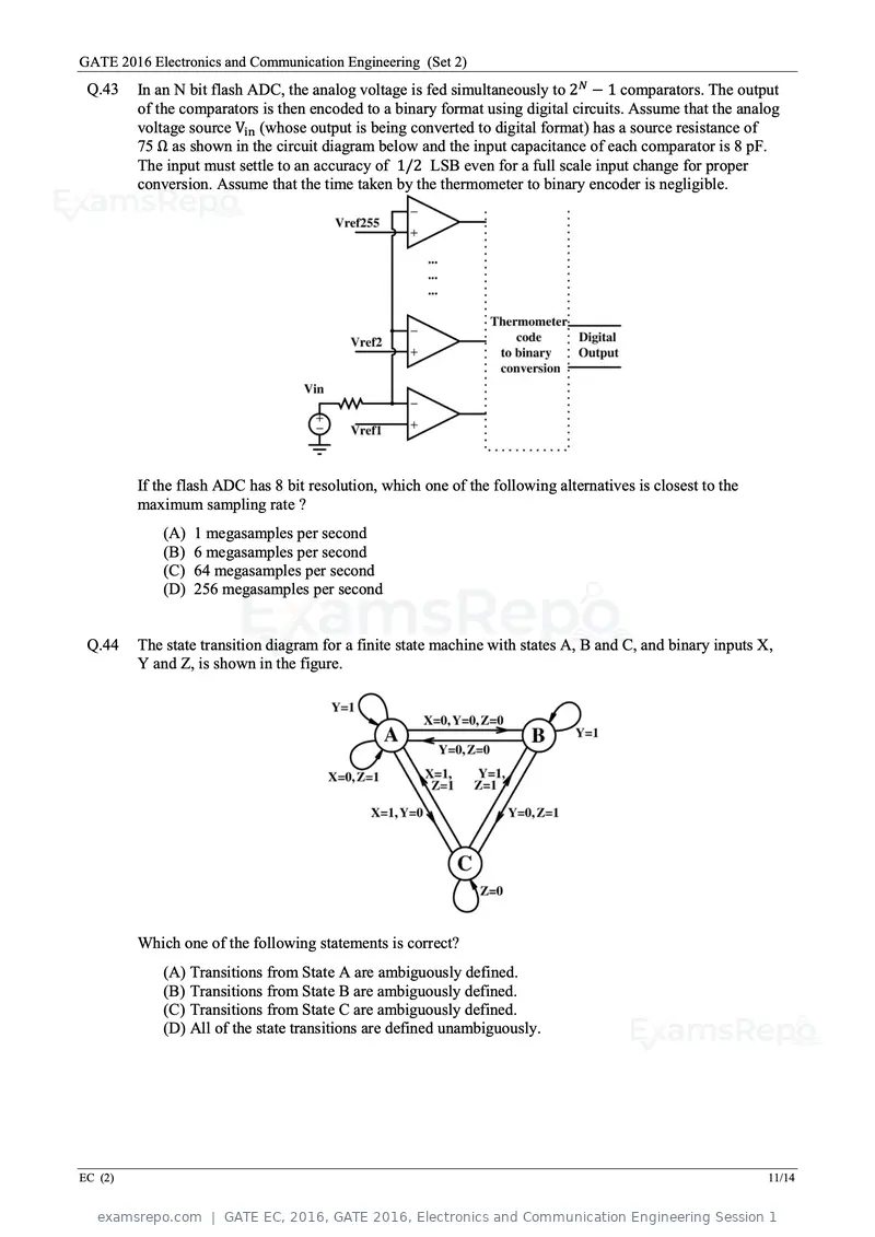
Text of page 35
GATE 2016 Electronics and Communication Engineering (Set 2)
 Q.43    In an N bit flash ADC, the analog voltage is fed simultaneously to 2N − 1 comparators. The output
         of the comparators is then encoded to a binary format using digital circuits. Assume that the analog
         voltage source Vin (whose output is being converted to digital format) has a source resistance of
         75 Ω as shown in the circuit diagram below and the input capacitance of each comparator is 8 pF.
         The input must settle to an accuracy of 1/2 LSB even for a full scale input change for proper
         conversion. Assume that the time taken by the thermometer to binary encoder is negligible.


         If the flash ADC has 8 bit resolution, which one of the following alternatives is closest to the
         maximum sampling rate ?
             (A) 1 megasamples per second
             (B) 6 megasamples per second
             (C) 64 megasamples per second
             (D) 256 megasamples per second


 Q.44    The state transition diagram for a finite state machine with states A, B and C, and binary inputs X,
         Y and Z, is shown in the figure.


         Which one of the following statements is correct?
             (A) Transitions from State A are ambiguously defined.
             (B) Transitions from State B are ambiguously defined.
             (C) Transitions from State C are ambiguously defined.
             (D) All of the state transitions are defined unambiguously.


EC (2)                                                                                                      11/14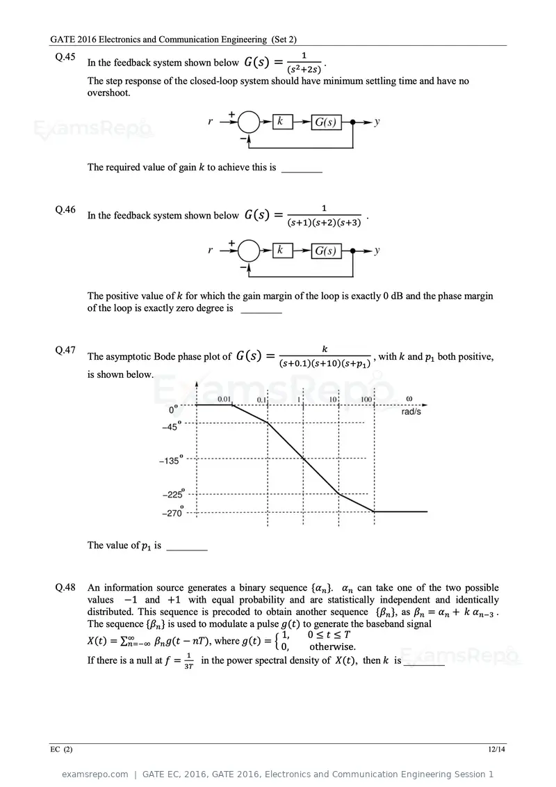
Text of page 36
GATE 2016 Electronics and Communication Engineering (Set 2)
 Q.45                                                         1
         In the feedback system shown below G(s) =                   .
                                                         (s 2 +2s)
         The step response of the closed-loop system should have minimum settling time and have no
         overshoot.


         The required value of gain k to achieve this is ________


 Q.46                                                                1
         In the feedback system shown below G(s) =                          .
                                                         (s+1)(s+2)(s+3)


         The positive value of k for which the gain margin of the loop is exactly 0 dB and the phase margin
         of the loop is exactly zero degree is ________


 Q.47                                                                k
         The asymptotic Bode phase plot of G(s) =                               , with k and p1 both positive,
                                                       (s+0.1)(s+10)(s+p1 )
         is shown below.


         The value of p1 is ________


 Q.48    An information source generates a binary sequence {αn }. αn can take one of the two possible
         values −1 and +1 with equal probability and are statistically independent and identically
         distributed. This sequence is precoded to obtain another sequence {βn }, as βn = αn + k αn−3 .
         The sequence {βn } is used to modulate a pulse g(t) to generate the baseband signal
                                                         1,     0≤t≤T
         X(t) = ∑∞  n=−∞ βn g(t − nT), where g(t) = � 0,        otherwise.
                                    1
         If there is a null at f = 3T in the power spectral density of X(t), then k is ________


EC (2)                                                                                                      12/14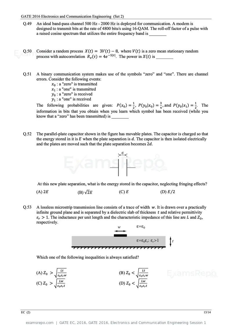
Text of page 37
GATE 2016 Electronics and Communication Engineering (Set 2)
 Q.49    An ideal band-pass channel 500 Hz - 2000 Hz is deployed for communication. A modem is
         designed to transmit bits at the rate of 4800 bits/s using 16-QAM. The roll-off factor of a pulse with
         a raised cosine spectrum that utilizes the entire frequency band is ________


 Q.50    Consider a random process X(t) = 3V(t) − 8, where V(t) is a zero mean stationary random
         process with autocorrelation Rv (τ) = 4e −5|τ| . The power in X(t) is ________


 Q.51    A binary communication system makes use of the symbols “zero” and “one”. There are channel
         errors. Consider the following events:
                  x0 : a "zero" is transmitted
                  x1 : a "one" is transmitted
                  y0 : a "zero" is received
                  y1 : a "one" is received
                                                              1            3                  1
         The following probabilities are given: P(x0 ) = , P(y0 |x0 ) = , and P(y0 |x1 ) = . The
                                                              2            4                  2
         information in bits that you obtain when you learn which symbol has been received (while you
         know that a “zero” has been transmitted) is ________


 Q.52    The parallel-plate capacitor shown in the figure has movable plates. The capacitor is charged so that
         the energy stored in it is E when the plate separation is d. The capacitor is then isolated electrically
         and the plates are moved such that the plate separation becomes 2d.


         At this new plate separation, what is the energy stored in the capacitor, neglecting fringing effects?
         (A) 2E                  (B) √2E                   (C) E                    (D) E ⁄2


 Q.53    A lossless microstrip transmission line consists of a trace of width w. It is drawn over a practically
         infinite ground plane and is separated by a dielectric slab of thickness t and relative permittivity
         εr > 1. The inductance per unit length and the characteristic impedance of this line are L and Z0 ,
         respectively.


         Which one of the following inequalities is always satisfied?


                       Lt                                               Lt
         (A) Z0 > �ε ε w                                   (B) Z0 < �ε ε w
                      0 r                                               0 r

                      Lw                                                Lw
         (C) Z0 > �ε ε t                                   (D) Z0 < �ε ε t
                      0 r                                               0 r


EC (2)                                                                                                        13/14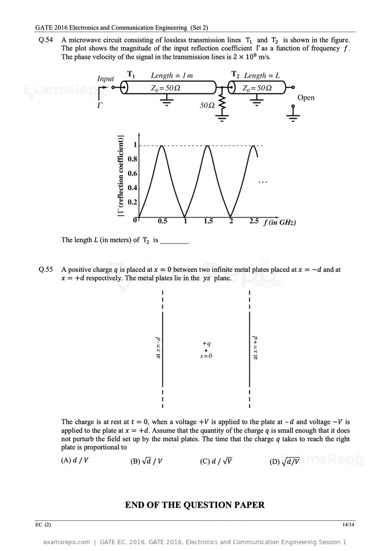
Text of page 38
GATE 2016 Electronics and Communication Engineering (Set 2)
 Q.54    A microwave circuit consisting of lossless transmission lines T1 and T2 is shown in the figure.
         The plot shows the magnitude of the input reflection coefficient Γ as a function of frequency f.
         The phase velocity of the signal in the transmission lines is 2 × 10⁸ m/s.


         The length L (in meters) of T2 is ________


 Q.55    A positive charge q is placed at x = 0 between two infinite metal plates placed at x = −d and at
         x = +d respectively. The metal plates lie in the yz plane.


         The charge is at rest at t = 0, when a voltage +V is applied to the plate at – d and voltage −V is
         applied to the plate at x = +d. Assume that the quantity of the charge q is small enough that it does
         not perturb the field set up by the metal plates. The time that the charge q takes to reach the right
         plate is proportional to
         (A) d / V               (B) √d / V              (C) d / √V              (D) �d/V


                               END OF THE QUESTION PAPER

EC (2)                                                                                                      14/14
Text of page 39
Q. No Type Section       Key      Marks
  1   MCQ    GA           C        1
  2   MCQ    GA           B        1
  3   MCQ    GA           C        1
  4   MCQ    GA           C        1
  5   MCQ    GA           B        1
  6   MCQ    GA           D        2
  7   MCQ    GA           A        2
  8   MCQ    GA           D        2
  9   MCQ    GA           C        2
 10 MCQ      GA           B        2
  1   NAT   EC-2     0.95 : 1.05   1
  2   NAT   EC-2       0.0 : 0.0   1
  3   MCQ EC-2            B        1
  4   MCQ EC-2            C        1
  5   NAT   EC-2       90 : 90     1
  6   MCQ EC-2            B        1
  7   MCQ EC-2            D        1
  8   NAT   EC-2     0.30 : 0.34   1
  9   NAT   EC-2     2.98 : 3.02   1
 10   NAT   EC-2     0.24 : 0.26   1
 11 MCQ EC-2              D        1
 12 MCQ EC-2              D        1
 13   NAT   EC-2     0.25 : 0.25   1
 14   NAT   EC-2      570 : 610    1
 15 MCQ EC-2              A        1
 16 MCQ EC-2              B        1
 17   NAT   EC-2     1.45 : 1.55   1
 18 MCQ EC-2              A        1
 19   NAT   EC-2     0.96 : 1.04   1
 20 MCQ EC-2              A        1
 21   NAT   EC-2     1.74 : 1.76   1
 22   NAT   EC-2     15.9 : 16.1   1
 23 MCQ EC-2              A        1
 24 MCQ EC-2              D        1
 25   NAT   EC-2        32:33      1
 26   NAT   EC-2       0.6 : 0.7   2
 27   NAT   EC-2     -0.03 : 0.03  2
 28   NAT   EC-2     0.32 : 0.34   2
 29   NAT   EC-2       2.9 : 3.1   2
 30 MCQ EC-2              D        2
 31   NAT   EC-2       4.9 : 5.1   2
 32   NAT   EC-2     0.04 : 0.06   2
 33   NAT   EC-2       5.9 : 6.1   2
 34   NAT   EC-2      99 : 101     2
 35 MCQ EC-2              B        2
 36 MCQ EC-2              C        2
 37   NAT   EC-2        30:34      2
 38   NAT   EC-2     1.18 : 1.22   2
 39   NAT   EC-2       1.9 : 2.2   2
Text of page 40
40   NAT   EC-2     0.7 : 0.9     2
41   NAT   EC-2    400 : 425      2
42   MCQ   EC-2        A          2
43   MCQ   EC-2        A          2
44   MCQ   EC-2         C         2
45   NAT   EC-2    0.95 : 1.05    2
46   NAT   EC-2    59.5 : 60.5    2
47   NAT   EC-2    0.95 : 1.05    2
48   NAT   EC-2   -1.01 : -0.99   2
49   NAT   EC-2    0.24 : 0.26    2
50   NAT   EC-2     99 : 101      2
51   NAT   EC-2    0.80 : 0.82    2
52   MCQ   EC-2        A          2
53   MCQ   EC-2        B          2
54   NAT   EC-2    0.09 : 0.11    2
55   MCQ   EC-2         C         2

Text of page 41
GATE 2016                                                                        General Aptitude - GA Set-4


Q. 1 – Q. 5 carry one mark each.
Q.1    An apple costs Rs. 10. An onion costs Rs. 8.

       Select the most suitable sentence with respect to grammar and usage.
      (A) The price of an apple is greater than an onion.

      (B) The price of an apple is more than onion.

      (C) The price of an apple is greater than that of an onion.

      (D) Apples are more costlier than onions.


Q.2    The Buddha said, “Holding on to anger is like grasping a hot coal with the intent of throwing it at
       someone else; you are the one who gets burnt.”

       Select the word below which is closest in meaning to the word underlined above.

      (A) burning               (B) igniting             (C) clutching            (D) flinging


Q.3    M has a son Q and a daughter R. He has no other children. E is the mother of P and daughter-in-
       law of M. How is P related to M?

      (A) P is the son-in-law of M.                      (B) P is the grandchild of M.

      (C) P is the daughter-in law of M.                 (D) P is the grandfather of M.


Q.4    The number that least fits this set: (324, 441, 97 and 64) is ________.

      (A) 324                  (B) 441                   (C) 97                   (D) 64


Q.5    It takes 10 s and 15 s, respectively, for two trains travelling at different constant speeds to
       completely pass a telegraph post. The length of the first train is 120 m and that of the second train is
       150 m. The magnitude of the difference in the speeds of the two trains (in m/s) is ____________.

      (A) 2.0                  (B) 10.0                  (C) 12.0                 (D) 22.0


                                                                                                                  1/3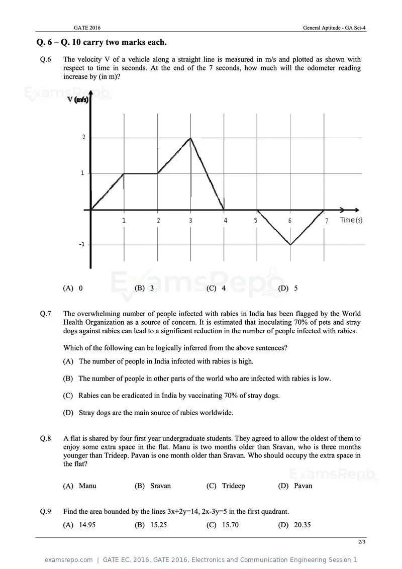
Text of page 42
GATE 2016                                                                      General Aptitude - GA Set-4

Q. 6 – Q. 10 carry two marks each.
Q.6   The velocity V of a vehicle along a straight line is measured in m/s and plotted as shown with
      respect to time in seconds. At the end of the 7 seconds, how much will the odometer reading
      increase by (in m)?


      (A) 0                   (B) 3                    (C) 4                   (D) 5


Q.7   The overwhelming number of people infected with rabies in India has been flagged by the World
      Health Organization as a source of concern. It is estimated that inoculating 70% of pets and stray
      dogs against rabies can lead to a significant reduction in the number of people infected with rabies.

      Which of the following can be logically inferred from the above sentences?
      (A) The number of people in India infected with rabies is high.

      (B) The number of people in other parts of the world who are infected with rabies is low.

      (C) Rabies can be eradicated in India by vaccinating 70% of stray dogs.

      (D) Stray dogs are the main source of rabies worldwide.


Q.8   A flat is shared by four first year undergraduate students. They agreed to allow the oldest of them to
      enjoy some extra space in the flat. Manu is two months older than Sravan, who is three months
      younger than Trideep. Pavan is one month older than Sravan. Who should occupy the extra space in
      the flat?

      (A) Manu                (B) Sravan               (C) Trideep             (D) Pavan


Q.9   Find the area bounded by the lines 3x+2y=14, 2x-3y=5 in the first quadrant.
      (A) 14.95               (B) 15.25                (C) 15.70               (D) 20.35

                                                                                                               2/3
Text of page 43
GATE 2016                                                                            General Aptitude - GA Set-4


Q.10   A straight line is fit to a data set (ln x, y). This line intercepts the abscissa at ln x = 0.1 and has a
       slope of −0.02. What is the value of y at x = 5 from the fit?

       (A) −0.030                (B) −0.014                (C) 0.014                  (D) 0.030


                               END OF THE QUESTION PAPER


                                                                                                                      3/3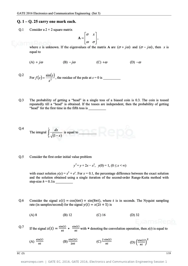
Text of page 44
GATE 2016 Electronics and Communication Engineering (Set 3)
Q. 1 – Q. 25 carry one mark each.
Q.1 Consider a 2 × 2 square matrix
σ x
A= ,
ω σ
where x is unknown. If the eigenvalues of the matrix A are (σ + jω ) and (σ − jω ) , then x is
equal to
(A) + jω (B) − jω (C) +ω (D) −ω
Q.2 sin ( z )
For f ( z ) = , the residue of the pole at z = 0 is __________
z2
Q.3 The probability of getting a “head” in a single toss of a biased coin is 0.3. The coin is tossed
repeatedly till a “head” is obtained. If the tosses are independent, then the probability of getting
“head” for the first time in the fifth toss is __________
Q.4 1
dx
The integral ∫ (1 − x) is equal to __________
0
Q.5 Consider the first order initial value problem
y' = y + 2x − x2, y(0) = 1, (0 ≤ x < ∞)
with exact solution y(x) = x2 + ex. For x = 0.1, the percentage difference between the exact solution
and the solution obtained using a single iteration of the second-order Runge-Kutta method with
step-size h = 0.1is __________
Q.6 Consider the signal x(t) = cos(6πt) + sin(8πt), where t is in seconds. The Nyquist sampling
rate (in samples/second) for the signal y(t) = x(2t + 5) is
(A) 8 (B) 12 (C) 16 (D) 32
sin(t) sin(t)
Q.7 If the signal x(t) = ∗ with ∗ denoting the convolution operation, then x(t) is equal to
πt πt
sin(t) sin(2t) 2 sin(t) sin(t) 2
(A)
πt
(B)
2πt
(C)
πt (D) � �
πt
EC (3) 1/19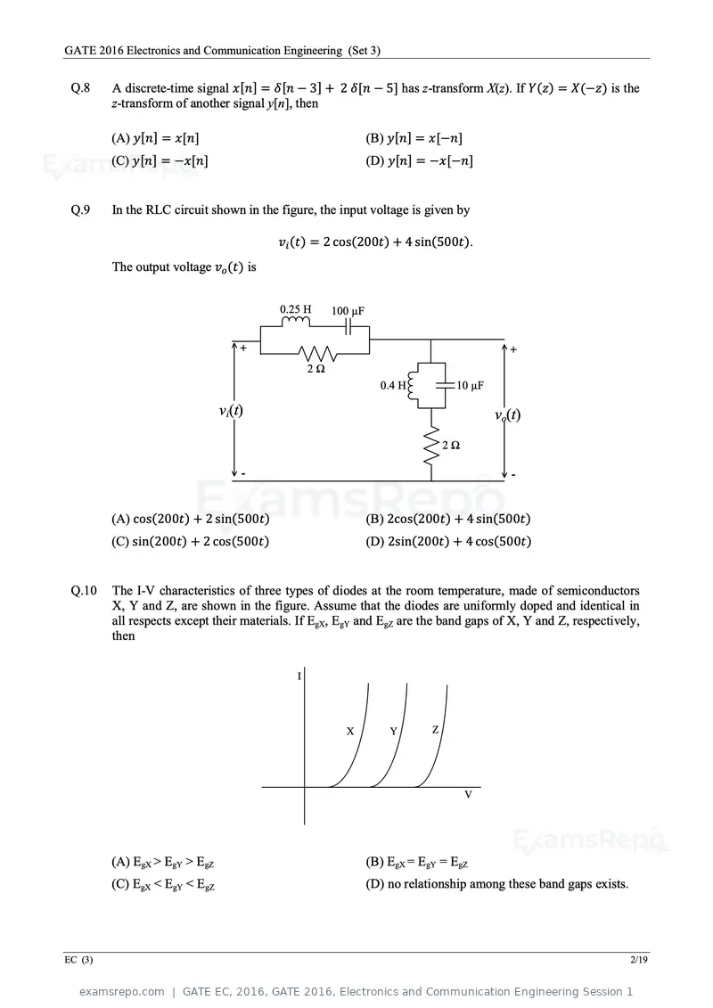
Text of page 45
GATE 2016 Electronics and Communication Engineering (Set 3)


 Q.8     A discrete-time signal x[n] = δ[n − 3] + 2 δ[n − 5] has z-transform X(z). If Y(z) = X(−z) is the
         z-transform of another signal y[n], then

         (A) y[n] = x[n]                                       (B) y[n] = x[−n]
         (C) y[n] = −x[n]                                      (D) y[n] = −x[−n]


 Q.9     In the RLC circuit shown in the figure, the input voltage is given by

                                         vi (t) = 2 cos(200t) + 4 sin(500t).
         The output voltage vo (t) is


                                         0.25 H       100 µF


                                   +                                                      +
                                                 2Ω
                                                                 0.4 H          10 µF

                               vi(t)                                                    vo(t)
                                                                               2Ω

                                   -                                                       -


         (A) cos(200t) + 2 sin(500t)                           (B) 2cos(200t) + 4 sin(500t)
         (C) sin(200t) + 2 cos(500t)                           (D) 2sin(200t) + 4 cos(500t)


 Q.10    The I-V characteristics of three types of diodes at the room temperature, made of semiconductors
         X, Y and Z, are shown in the figure. Assume that the diodes are uniformly doped and identical in
         all respects except their materials. If EgX, EgY and EgZ are the band gaps of X, Y and Z, respectively,
         then


                                             I


                                                        X          Y       Z


                                                                                    V


         (A) EgX > EgY > EgZ                                   (B) EgX = EgY = EgZ
         (C) EgX < EgY < EgZ                                   (D) no relationship among these band gaps exists.


EC (3)                                                                                                             2/19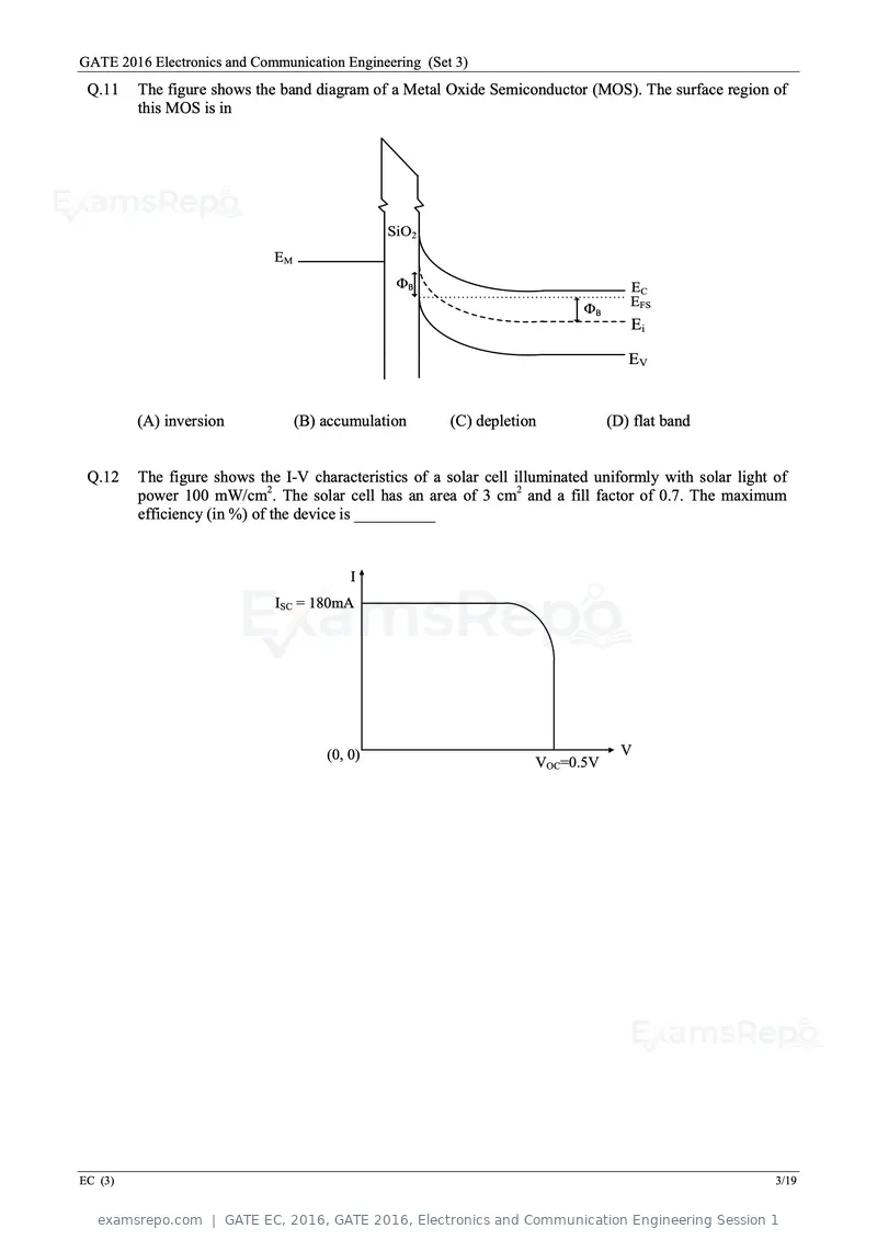
Text of page 46
GATE 2016 Electronics and Communication Engineering (Set 3)
 Q.11    The figure shows the band diagram of a Metal Oxide Semiconductor (MOS). The surface region of
         this MOS is in


                                               SiO2
                             EM
                                                ΦB                                  EC
                                                                                    EFS
                                                                            ΦB
                                                                                    Ei

                                                                                    EV


         (A) inversion            (B) accumulation      (C) depletion            (D) flat band


 Q.12    The figure shows the I-V characteristics of a solar cell illuminated uniformly with solar light of
         power 100 mW/cm2. The solar cell has an area of 3 cm2 and a fill factor of 0.7. The maximum
         efficiency (in %) of the device is __________


                                          I
                             ISC = 180mA


                                      (0, 0)                                       V
                                                                     VOC=0.5V


EC (3)                                                                                                   3/19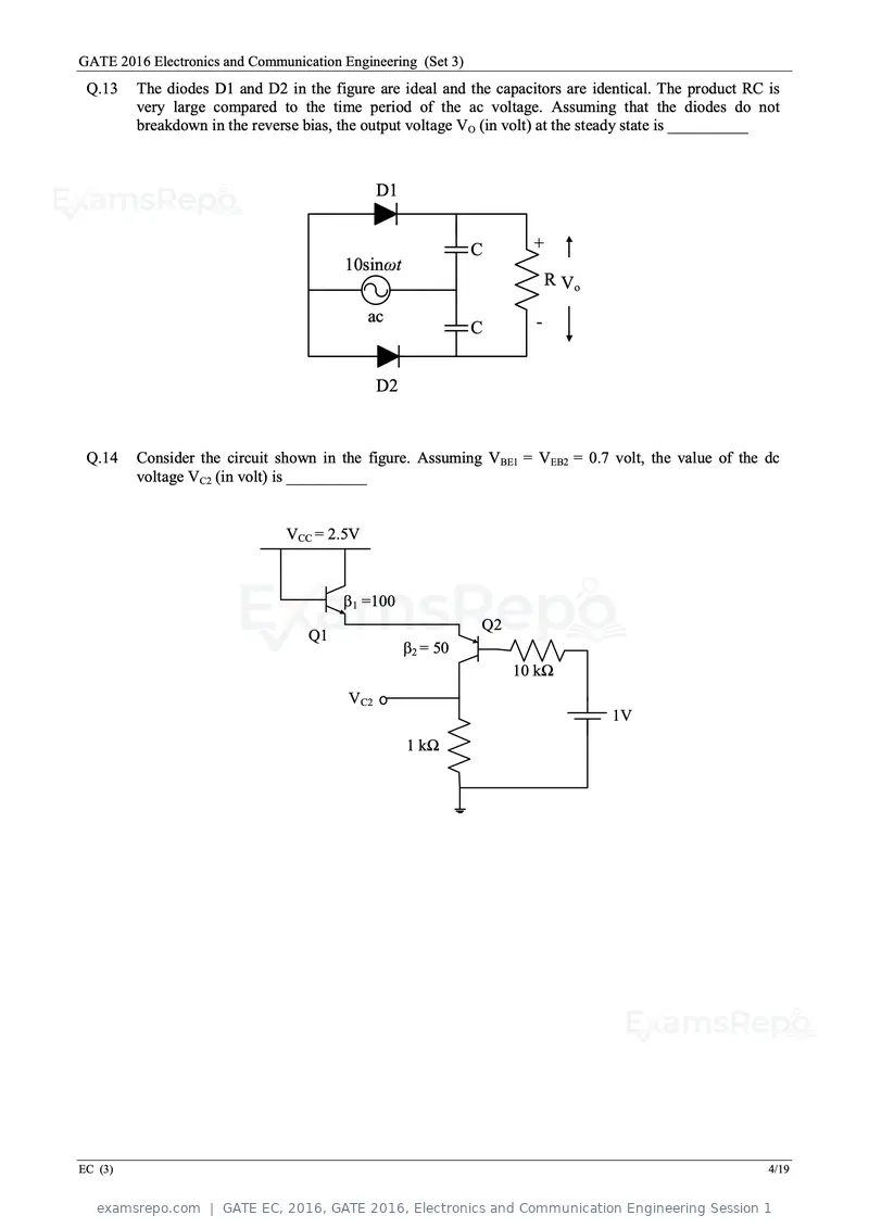
Text of page 47
GATE 2016 Electronics and Communication Engineering (Set 3)
 Q.13    The diodes D1 and D2 in the figure are ideal and the capacitors are identical. The product RC is
         very large compared to the time period of the ac voltage. Assuming that the diodes do not
         breakdown in the reverse bias, the output voltage VO (in volt) at the steady state is __________


                                               D1


                                                              C      +
                                        10sinωt
                                                                         R Vo

                                            ac                       -
                                                              C


                                               D2


 Q.14    Consider the circuit shown in the figure. Assuming VBE1 = VEB2 = 0.7 volt, the value of the dc
         voltage VC2 (in volt) is __________


                               VCC = 2.5V


                                        β1 =100
                                                              Q2
                                   Q1
                                                    β2 = 50
                                                                   10 kΩ
                                         VC2
                                                                                1V
                                                    1 kΩ


EC (3)                                                                                                 4/19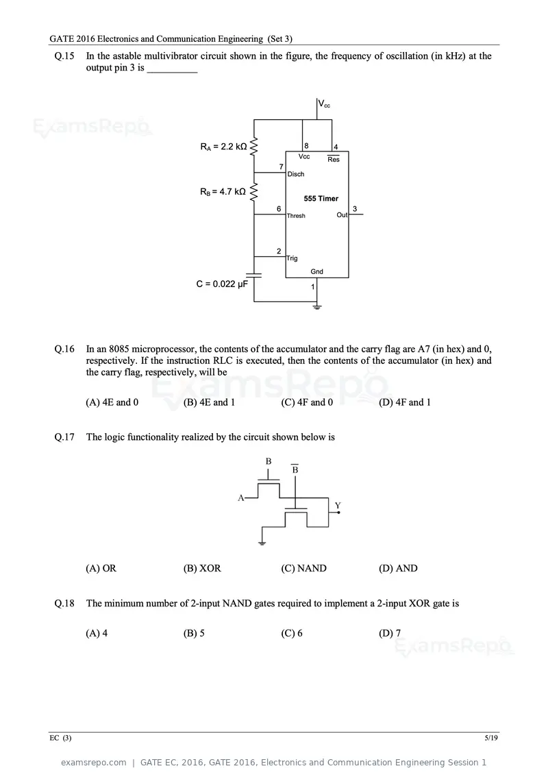
Text of page 48
GATE 2016 Electronics and Communication Engineering (Set 3)
 Q.15    In the astable multivibrator circuit shown in the figure, the frequency of oscillation (in kHz) at the
         output pin 3 is __________


                                                                              Vcc


                                     RA = 2.2 kΩ                     8              4
                                                                    Vcc         Res
                                                         7
                                                             Disch

                                     RB = 4.7 kΩ
                                                                     555 Timer
                                                        6                                 3
                                                             Thresh                 Out


                                                        2
                                                             Trig

                                                                          Gnd
                                    C = 0.022 µF                          1


 Q.16    In an 8085 microprocessor, the contents of the accumulator and the carry flag are A7 (in hex) and 0,
         respectively. If the instruction RLC is executed, then the contents of the accumulator (in hex) and
         the carry flag, respectively, will be

         (A) 4E and 0            (B) 4E and 1               (C) 4F and 0                      (D) 4F and 1


 Q.17    The logic functionality realized by the circuit shown below is


         (A) OR                  (B) XOR                    (C) NAND                          (D) AND


 Q.18    The minimum number of 2-input NAND gates required to implement a 2-input XOR gate is

         (A) 4                   (B) 5                      (C) 6                             (D) 7


EC (3)                                                                                                       5/19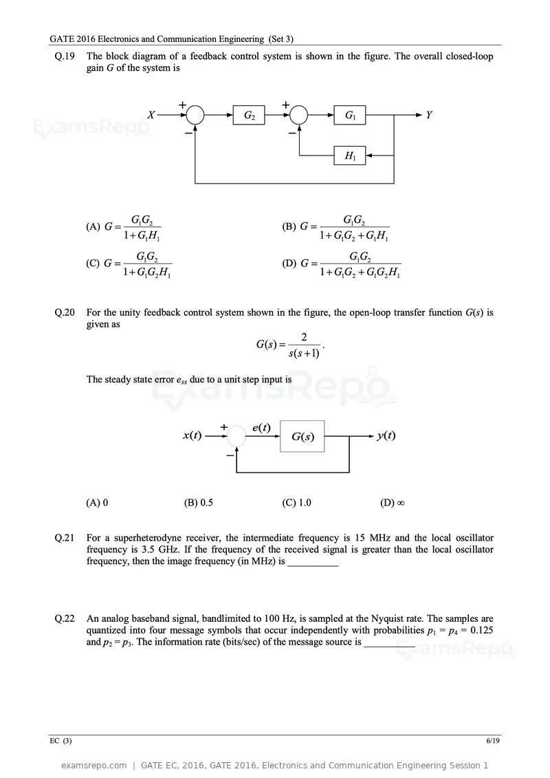
Text of page 49
GATE 2016 Electronics and Communication Engineering (Set 3)
 Q.19    The block diagram of a feedback control system is shown in the figure. The overall closed-loop
         gain G of the system is


                                 +                           +
                         X                        G2                            G1               Y
                                  −                              −
                                                                                H1


                     G1G2                                                        G1G2
         (A) G =                                             (B) G =
                   1 + G1 H1                                               1 + G1G2 + G1 H1
                       G1G2                                                       G1G2
         (C) G =                                             (D) G =
                   1 + G1G2 H1                                             1 + G1G2 + G1G2 H1


 Q.20    For the unity feedback control system shown in the figure, the open-loop transfer function G(s) is
         given as
                                                                      2
                                                       G (s) =              .
                                                                 s ( s + 1)

         The steady state error ess due to a unit step input is


                                            +       e(t)
                                  x(t)                           G(s)                   y(t)
                                             −


         (A) 0                    (B) 0.5                    (C) 1.0                     (D) ∞


 Q.21    For a superheterodyne receiver, the intermediate frequency is 15 MHz and the local oscillator
         frequency is 3.5 GHz. If the frequency of the received signal is greater than the local oscillator
         frequency, then the image frequency (in MHz) is __________


 Q.22    An analog baseband signal, bandlimited to 100 Hz, is sampled at the Nyquist rate. The samples are
         quantized into four message symbols that occur independently with probabilities p1 = p4 = 0.125
         and p2 = p3. The information rate (bits/sec) of the message source is __________


EC (3)                                                                                                   6/19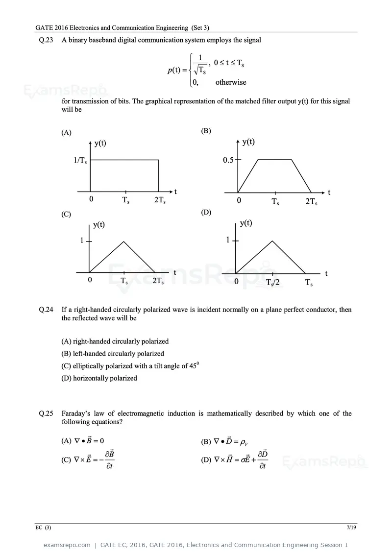
Text of page 50
GATE 2016 Electronics and Communication Engineering (Set 3)
Q.23 A binary baseband digital communication system employs the signal
1
, 0 ≤ t ≤ TS
p ( t ) = TS
0,
otherwise
for transmission of bits. The graphical representation of the matched filter output y(t) for this signal
will be
(A) (B)
y(t) y(t)
1/Ts 0.5
t t
0 Ts 2Ts 0 Ts 2Ts
(C) (D)
y(t) y(t)
1 1
t t
0 Ts 2Ts 0 Ts/2 Ts
Q.24 If a right-handed circularly polarized wave is incident normally on a plane perfect conductor, then
the reflected wave will be
(A) right-handed circularly polarized
(B) left-handed circularly polarized
(C) elliptically polarized with a tilt angle of 450
(D) horizontally polarized
Q.25 Faraday’s law of electromagnetic induction is mathematically described by which one of the
following equations?
(A) ∇ • B = 0 (B) ∇ • D = ρV
∂B ∂D
(C) ∇ × E = − (D) ∇ × H = σE +
∂t ∂t
EC (3) 7/19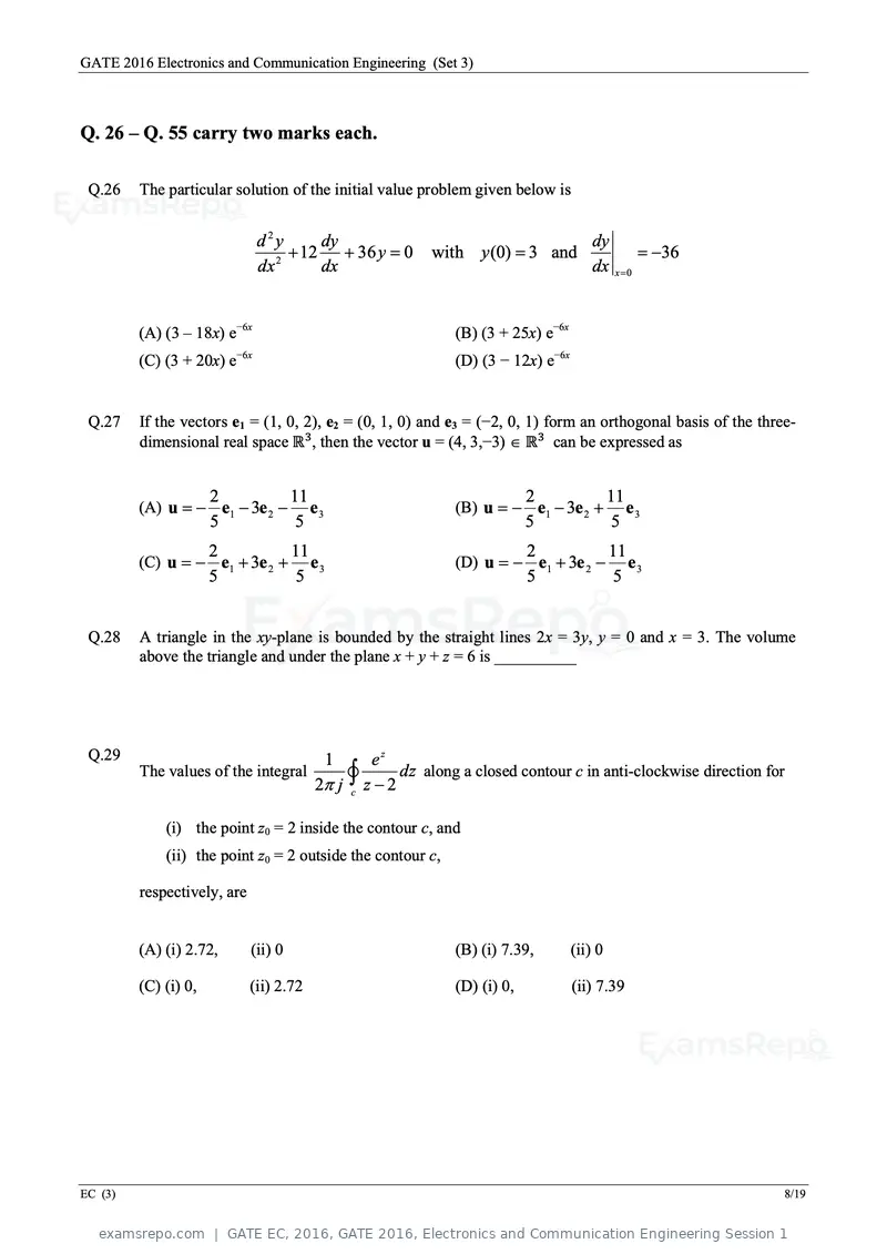
Text of page 51
GATE 2016 Electronics and Communication Engineering (Set 3)
Q. 26 – Q. 55 carry two marks each.
Q.26 The particular solution of the initial value problem given below is
d2y dy dy
2
+ 12 + 36 y 0
=with =and
y (0) 3 =
−36
dx dx dx x =0
(A) (3 – 18x) e−6x (B) (3 + 25x) e−6x
(C) (3 + 20x) e−6x (D) (3 − 12x) e−6x
Q.27 If the vectors e1 = (1, 0, 2), e2 = (0, 1, 0) and e3 = (−2, 0, 1) form an orthogonal basis of the three-
dimensional real space ℝ3 , then the vector u = (4, 3,−3) ∈ ℝ3 can be expressed as
2 11 2 11
(A) u = − e1 − 3e 2 − e3 (B) u = − e1 − 3e 2 + e3
5 5 5 5
2 11 2 11
(C) u = − e1 + 3e 2 + e3 (D) u = − e1 + 3e 2 − e3
5 5 5 5
Q.28 A triangle in the xy-plane is bounded by the straight lines 2x = 3y, y = 0 and x = 3. The volume
above the triangle and under the plane x + y + z = 6 is __________
Q.29 1 ez
2π j ∫c z − 2
The values of the integral dz along a closed contour c in anti-clockwise direction for
(i) the point z0 = 2 inside the contour c, and
(ii) the point z0 = 2 outside the contour c,
respectively, are
(A) (i) 2.72, (ii) 0 (B) (i) 7.39, (ii) 0
(C) (i) 0, (ii) 2.72 (D) (i) 0, (ii) 7.39
EC (3) 8/19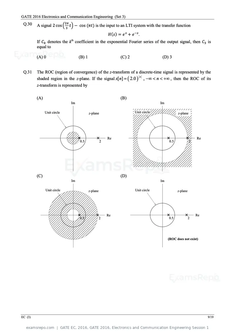
Text of page 52
GATE 2016 Electronics and Communication Engineering (Set 3)
 Q.30                        2π
         A signal 2 cos � 3 t� − cos (πt) is the input to an LTI system with the transfer function

                                                         H(s) = e s + e −s .
         If Ck denotes the kth coefficient in the exponential Fourier series of the output signal, then C3 is
         equal to

         (A) 0                         (B) 1                    (C) 2                    (D) 3


 Q.31    The ROC (region of convergence) of the z-transform of a discrete-time signal is represented by the
                                                =
         shaded region in the z-plane. If the signal x[n]             ( 2.0 ) n , −∞ < n < +∞ , then the ROC of its
         z-transform is represented by

         (A)                                                    (B)
                                  Im                                                    Im

               Unit circle                     z-plane                   Unit circle                z-plane


                                       ×0.5         ×2   Re                                  ×0.5        ×2     Re


         (C)                                                    (D)
                                  Im                                                    Im

               Unit circle                     z-plane                    Unit circle               z-plane


                                       ×0.5         ×2   Re                                  ×0.5        ×2    Re


                                                                                             (ROC does not exist)


EC (3)                                                                                                               9/19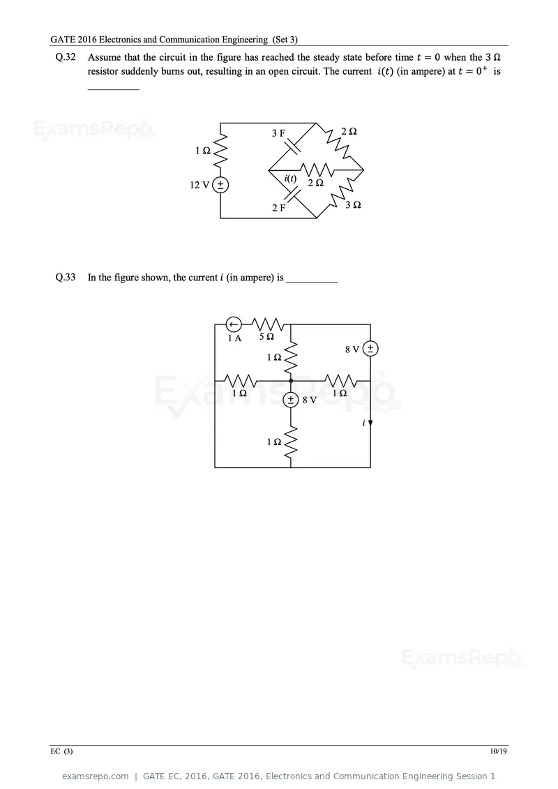
Text of page 53
GATE 2016 Electronics and Communication Engineering (Set 3)
 Q.32    Assume that the circuit in the figure has reached the steady state before time t = 0 when the 3 Ω
         resistor suddenly burns out, resulting in an open circuit. The current i(t) (in ampere) at t = 0+ is
         __________


                                                     3F                 2Ω
                                   1Ω

                                                         i(t)   2Ω
                                 12 V

                                                     2F                 3Ω


 Q.33    In the figure shown, the current i (in ampere) is __________


                                          1A      5Ω
                                                                        8V
                                                    1Ω


                                           1Ω                        1Ω
                                                                8V

                                                                             i
                                                    1Ω


EC (3)                                                                                                    10/19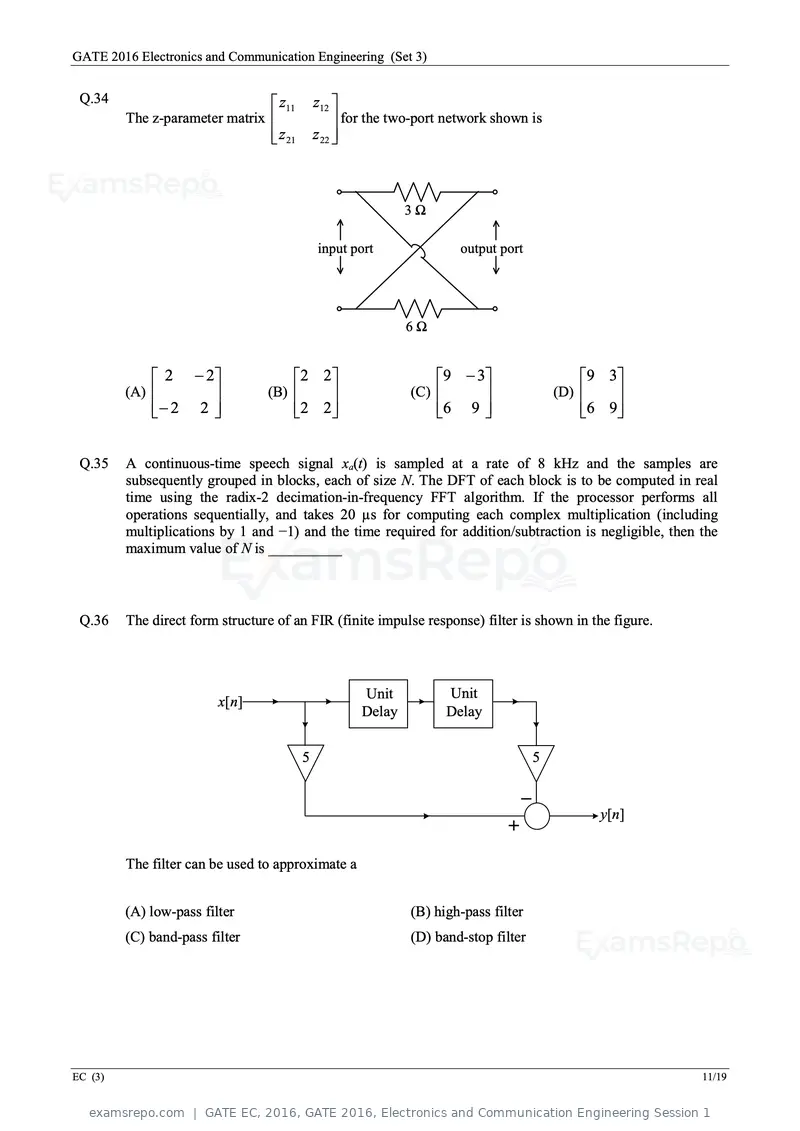
Text of page 54
GATE 2016 Electronics and Communication Engineering (Set 3)
Q.34 z11 z12
The z-parameter matrix for the two-port network shown is
z 21 z 22
3Ω
input port output port
6Ω
2 − 2 2 2 9 − 3 9 3
(A) (B) (C) (D)
− 2 2 2 2 6 9 6 9
Q.35 A continuous-time speech signal xa(t) is sampled at a rate of 8 kHz and the samples are
subsequently grouped in blocks, each of size N. The DFT of each block is to be computed in real
time using the radix-2 decimation-in-frequency FFT algorithm. If the processor performs all
operations sequentially, and takes 20 µs for computing each complex multiplication (including
multiplications by 1 and −1) and the time required for addition/subtraction is negligible, then the
maximum value of N is __________
Q.36 The direct form structure of an FIR (finite impulse response) filter is shown in the figure.
Unit Unit
x[n]
Delay Delay
5 5
−
y[n]
+
The filter can be used to approximate a
(A) low-pass filter (B) high-pass filter
(C) band-pass filter (D) band-stop filter
EC (3) 11/19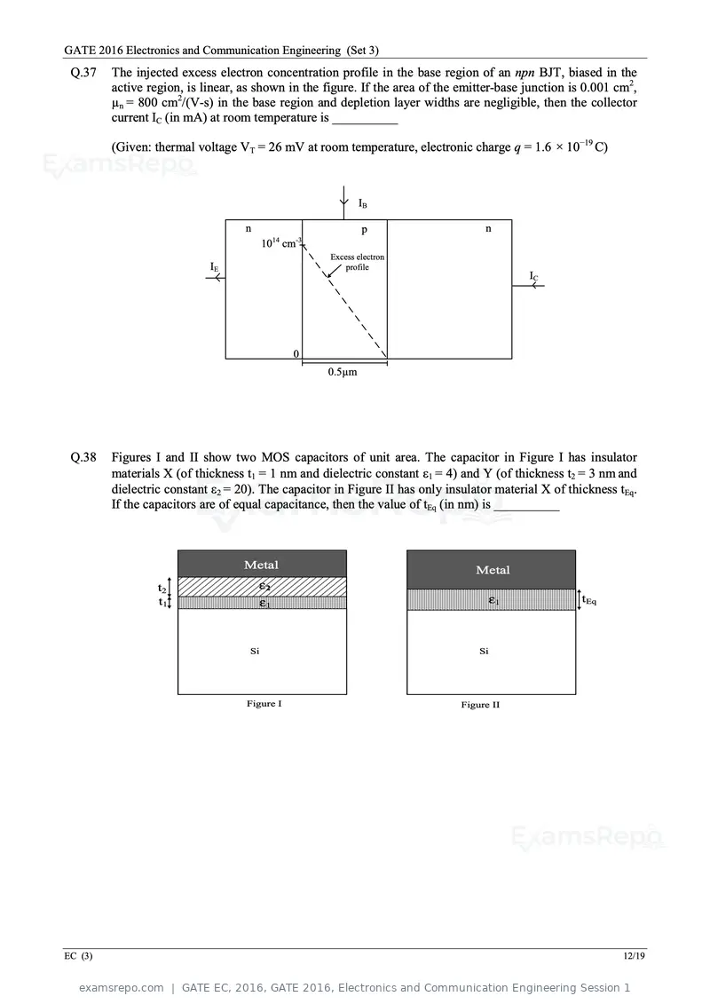
Text of page 55
GATE 2016 Electronics and Communication Engineering (Set 3)
 Q.37    The injected excess electron concentration profile in the base region of an npn BJT, biased in the
         active region, is linear, as shown in the figure. If the area of the emitter-base junction is 0.001 cm2,
         µn = 800 cm2/(V-s) in the base region and depletion layer widths are negligible, then the collector
         current IC (in mA) at room temperature is __________

         (Given: thermal voltage VT = 26 mV at room temperature, electronic charge q = 1.6 × 10⁻¹⁹ C)


                                                           IB

                                   n                        p                      n
                                       1014 cm-3
                                                    Excess electron
                            IE                          profile
                                                                                           IC


                                              0
                                                   0.5µm


 Q.38    Figures I and II show two MOS capacitors of unit area. The capacitor in Figure I has insulator
         materials X (of thickness t1 = 1 nm and dielectric constant ε1 = 4) and Y (of thickness t2 = 3 nm and
         dielectric constant ε2 = 20). The capacitor in Figure II has only insulator material X of thickness tEq.
         If the capacitors are of equal capacitance, then the value of tEq (in nm) is __________


                                   Metal                                         Metal
                  t2                   ε2
                  t1                   ε1                                           ε1                tEq


                                    SiSi                                          SiSi


                                   Figure I                                   Figure II


EC (3)                                                                                                        12/19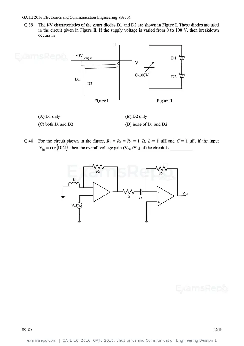
Text of page 56
GATE 2016 Electronics and Communication Engineering (Set 3)
 Q.39    The I-V characteristics of the zener diodes D1 and D2 are shown in Figure I. These diodes are used
         in the circuit given in Figure II. If the supply voltage is varied from 0 to 100 V, then breakdown
         occurs in

                                                      I

                             -80V
                                    -70V                                          D1
                                                               V

                                                               0-100V             D2
                               D1
                                     D2


                                           Figure I                      Figure II


         (A) D1 only                                      (B) D2 only
         (C) both D1and D2                                (D) none of D1 and D2


 Q.40    For the circuit shown in the figure, R1 = R2 = R3 = 1 Ω, L = 1 µH and C = 1 µF. If the input
                  ( )
         Vin = cos 106 t , then the overall voltage gain (Vout /Vin) of the circuit is __________


                                               R1
                                                                          R3
                           L

                                           -
                                                                          -            Vout
                                           +              R2
                                                                   C
                                                                          +
                          Vin


EC (3)                                                                                                  13/19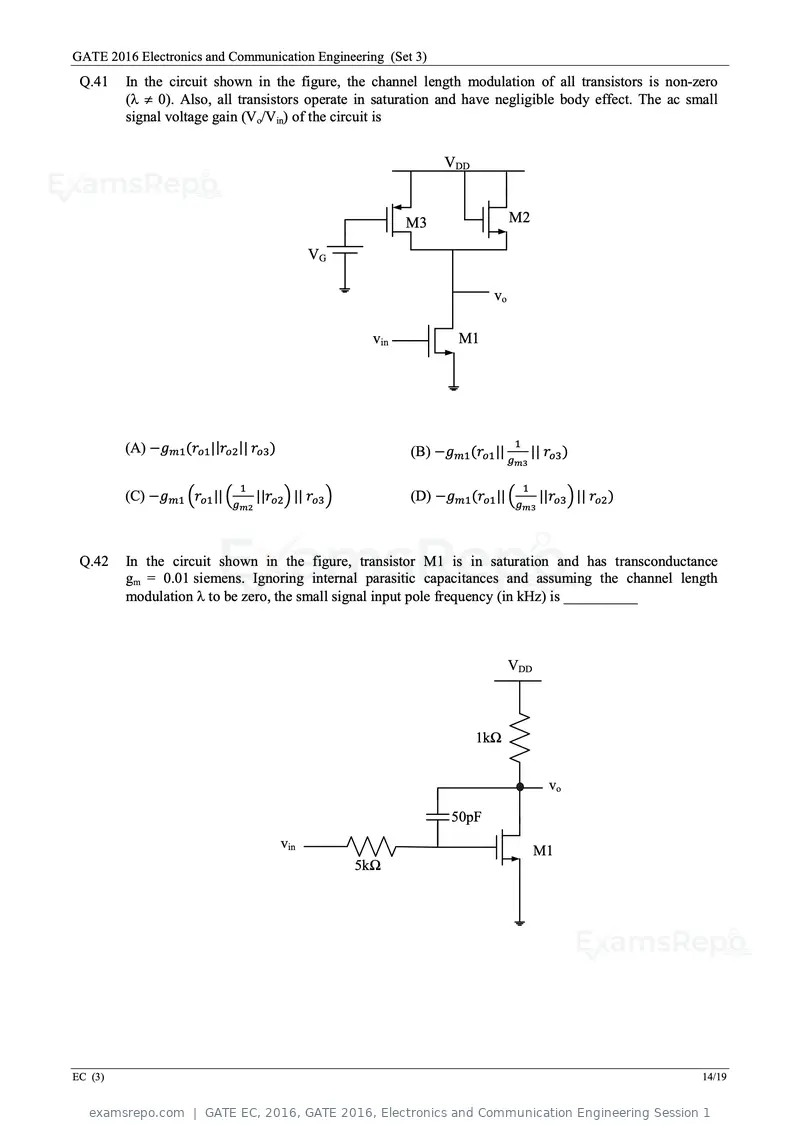
Text of page 57
GATE 2016 Electronics and Communication Engineering (Set 3)
 Q.41    In the circuit shown in the figure, the channel length modulation of all transistors is non-zero
         (λ ≠ 0). Also, all transistors operate in saturation and have negligible body effect. The ac small
         signal voltage gain (Vo/Vin) of the circuit is


                                                                   VDD


                                                              M3                 M2

                                              VG

                                                                            vo

                                                        vin           M1


         (A) −gm1 (ro1 ||ro2 || ro3 )                                             1
                                                              (B) −gm1 (ro1 ||       || ro3 )
                                                                                 gm3

                               1                                                    1
         (C) −gm1 �ro1 || �g       ||ro2 � || ro3 �           (D) −gm1 (ro1 || �g       ||ro3 � || ro2 )
                              m2                                                   m3


 Q.42    In the circuit shown in the figure, transistor M1 is in saturation and has transconductance
         gm = 0.01 siemens. Ignoring internal parasitic capacitances and assuming the channel length
         modulation λ to be zero, the small signal input pole frequency (in kHz) is __________


                                                                                 VDD


                                                                         1kΩ


                                                                                          vo

                                                                    50pF
                                        vin
                                                                                        M1
                                                      5kΩ


EC (3)                                                                                                     14/19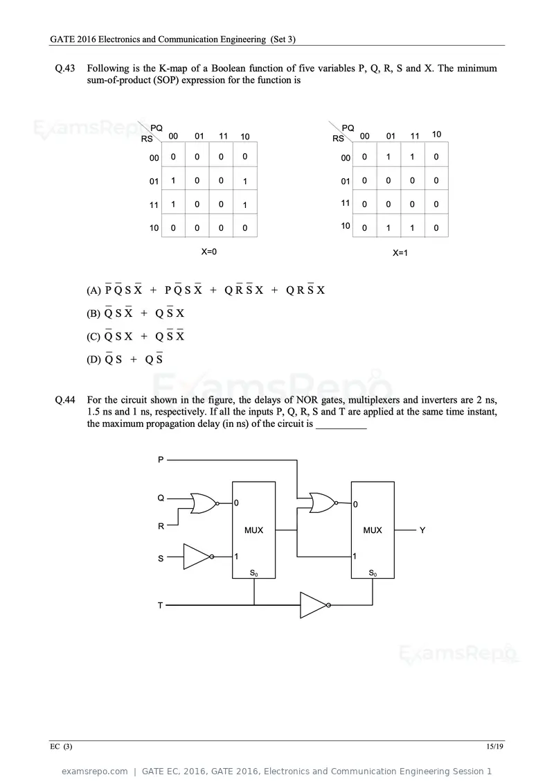
Text of page 58
GATE 2016 Electronics and Communication Engineering (Set 3)


 Q.43    Following is the K-map of a Boolean function of five variables P, Q, R, S and X. The minimum
         sum-of-product (SOP) expression for the function is


                        PQ                                              PQ
                           00       01        11       10                  00             01        11       10
                      RS                                              RS

                        00    0     0         0        0                00       0        1         1        0

                        01    1     0         0        1                01       0        0         0        0

                        11    1     0         0        1                11       0        0         0        0

                        10    0     0         0        0                10       0        1         1        0

                                        X=0                                                   X=1


         (A) P Q S X + P Q S X + Q R S X + Q R S X

         (B) Q S X + Q S X

         (C) Q S X + Q S X

         (D) Q S + Q S


 Q.44    For the circuit shown in the figure, the delays of NOR gates, multiplexers and inverters are 2 ns,
         1.5 ns and 1 ns, respectively. If all the inputs P, Q, R, S and T are applied at the same time instant,
         the maximum propagation delay (in ns) of the circuit is __________


                          P


                          Q
                                                   0                         0

                          R                            MUX                       MUX                     Y


                          S                        1                         1
                                                            S0                       S0


                          T


EC (3)                                                                                                            15/19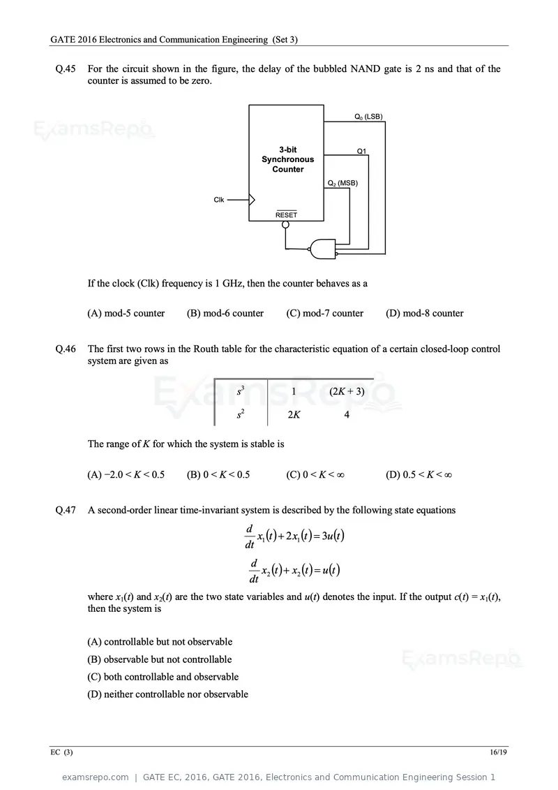
Text of page 59
GATE 2016 Electronics and Communication Engineering (Set 3)


 Q.45    For the circuit shown in the figure, the delay of the bubbled NAND gate is 2 ns and that of the
         counter is assumed to be zero.


                                                                                         Q0 (LSB)


                                                             3-bit                       Q1
                                                         Synchronous
                                                           Counter
                                                                              Q2 (MSB)

                                         Clk

                                                             RESET


         If the clock (Clk) frequency is 1 GHz, then the counter behaves as a

         (A) mod-5 counter        (B) mod-6 counter              (C) mod-7 counter                  (D) mod-8 counter


 Q.46    The first two rows in the Routh table for the characteristic equation of a certain closed-loop control
         system are given as

                                               s3                 1            (2K + 3)

                                               s2                2K                  4

         The range of K for which the system is stable is

         (A) −2.0 < K < 0.5       (B) 0 < K < 0.5                (C) 0 < K < ∞                      (D) 0.5 < K < ∞


 Q.47    A second-order linear time-invariant system is described by the following state equations

                                                       x1 (t ) + 2 x1 (t ) = 3u (t )
                                                    d
                                                    dt

                                                        x2 (t ) + x2 (t ) = u (t )
                                                     d
                                                     dt
         where x1(t) and x2(t) are the two state variables and u(t) denotes the input. If the output c(t) = x1(t),
         then the system is


         (A) controllable but not observable
         (B) observable but not controllable
         (C) both controllable and observable
         (D) neither controllable nor observable


EC (3)                                                                                                                  16/19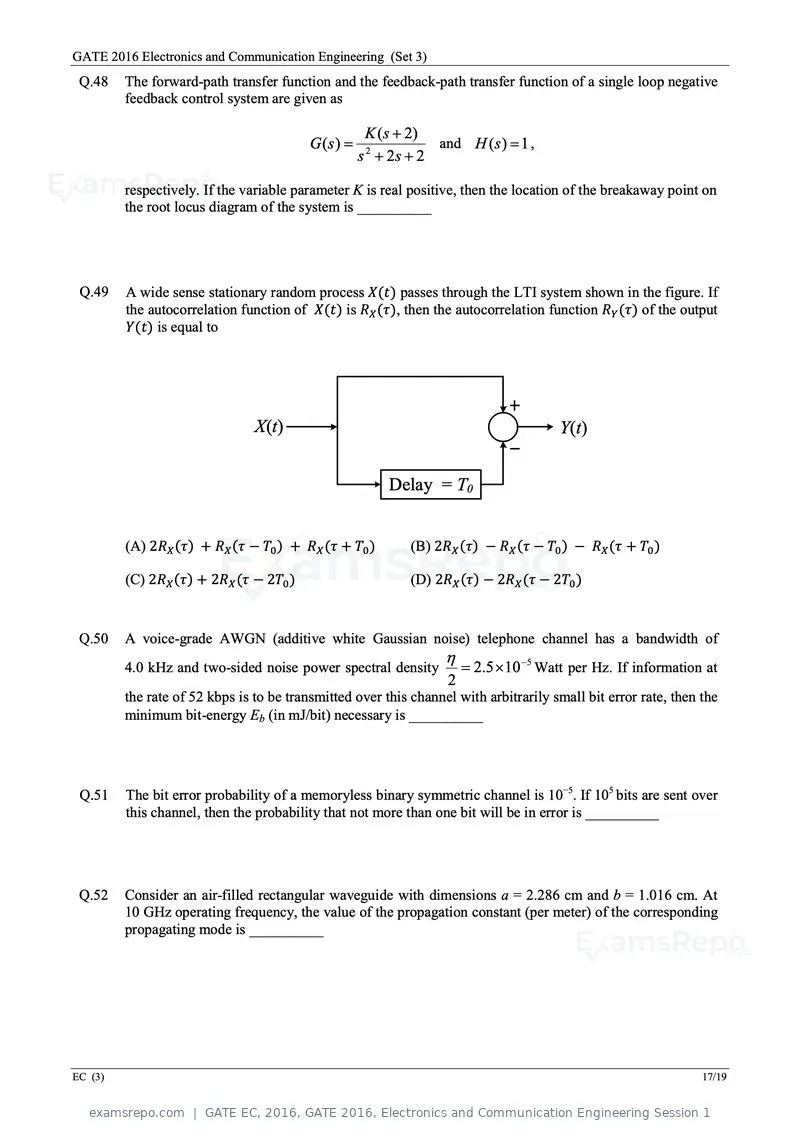
Text of page 60
GATE 2016 Electronics and Communication Engineering (Set 3)
 Q.48    The forward-path transfer function and the feedback-path transfer function of a single loop negative
         feedback control system are given as

                                                      K ( s + 2)
                                          G ( s) =                and H ( s ) = 1 ,
                                                     s 2 + 2s + 2

         respectively. If the variable parameter K is real positive, then the location of the breakaway point on
         the root locus diagram of the system is __________


 Q.49    A wide sense stationary random process X(t) passes through the LTI system shown in the figure. If
         the autocorrelation function of X(t) is RX (τ), then the autocorrelation function RY (τ) of the output
         Y(t) is equal to


                                X(t)                                                    Y(t)


                                                          Delay = T0


         (A) 2RX (τ) + RX (τ − T0 ) + RX (τ + T0 )           (B) 2RX (τ) − RX (τ − T0 ) − RX (τ + T0 )

         (C) 2RX (τ) + 2RX (τ − 2T0 )                        (D) 2RX (τ) − 2RX (τ − 2T0 )


 Q.50    A voice-grade AWGN (additive white Gaussian noise) telephone channel has a bandwidth of
                                                                   η
         4.0 kHz and two-sided noise power spectral density             = 2.5 ×10 −5 Watt per Hz. If information at
                                                                    2
         the rate of 52 kbps is to be transmitted over this channel with arbitrarily small bit error rate, then the
         minimum bit-energy Eb (in mJ/bit) necessary is __________


 Q.51    The bit error probability of a memoryless binary symmetric channel is 10−5. If 105 bits are sent over
         this channel, then the probability that not more than one bit will be in error is __________


 Q.52    Consider an air-filled rectangular waveguide with dimensions a = 2.286 cm and b = 1.016 cm. At
         10 GHz operating frequency, the value of the propagation constant (per meter) of the corresponding
         propagating mode is __________


EC (3)                                                                                                          17/19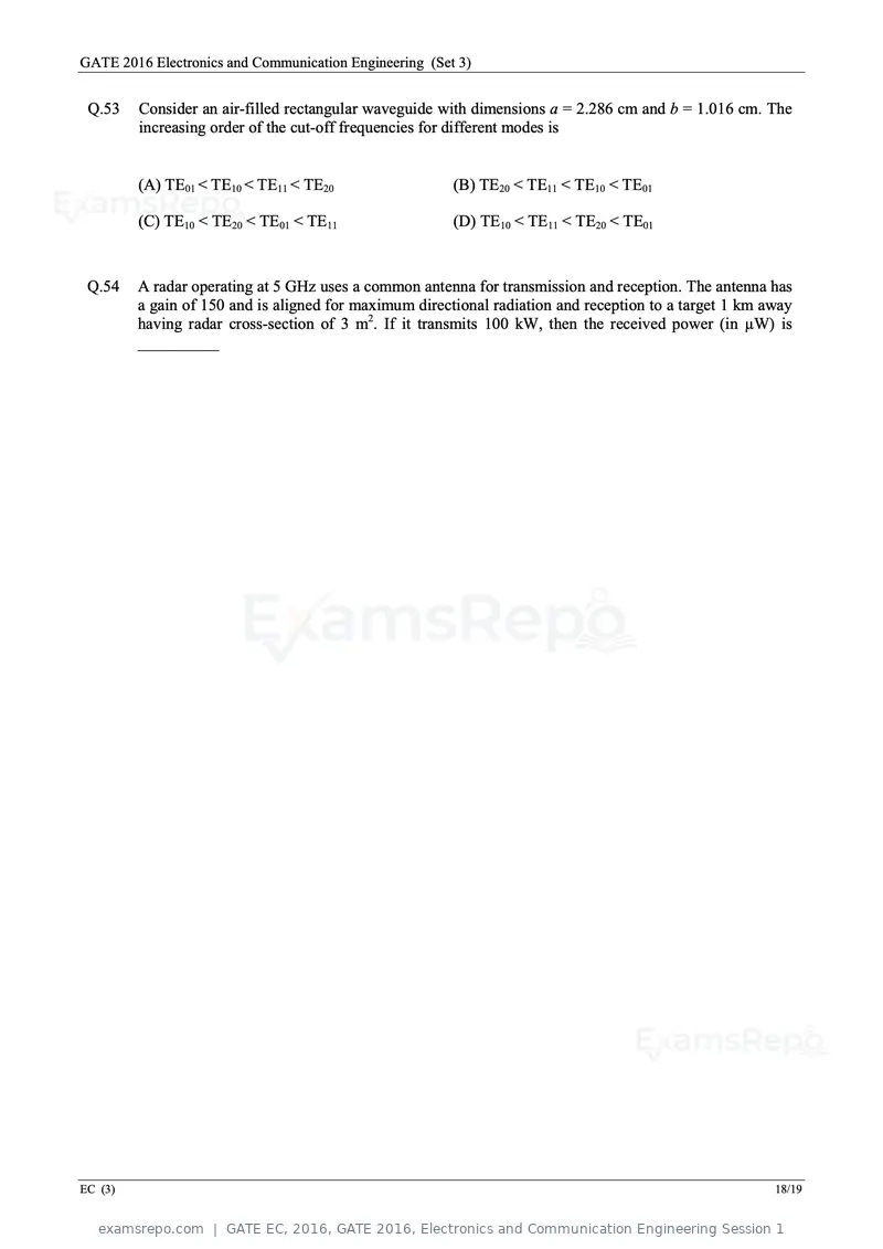
Text of page 61
GATE 2016 Electronics and Communication Engineering (Set 3)


 Q.53    Consider an air-filled rectangular waveguide with dimensions a = 2.286 cm and b = 1.016 cm. The
         increasing order of the cut-off frequencies for different modes is


         (A) TE01 < TE10 < TE11 < TE20                  (B) TE20 < TE11 < TE10 < TE01

         (C) TE10 < TE20 < TE01 < TE11                  (D) TE10 < TE11 < TE20 < TE01


 Q.54    A radar operating at 5 GHz uses a common antenna for transmission and reception. The antenna has
         a gain of 150 and is aligned for maximum directional radiation and reception to a target 1 km away
         having radar cross-section of 3 m2. If it transmits 100 kW, then the received power (in µW) is
         __________


EC (3)                                                                                                  18/19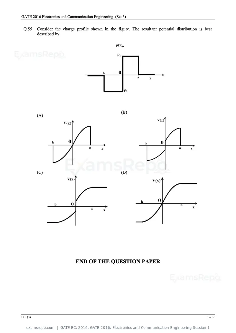
Text of page 62
GATE 2016 Electronics and Communication Engineering (Set 3)


 Q.55    Consider the charge profile shown in the figure. The resultant potential distribution is best
         described by


                                                        (B)
         (A)


         (C)                                            (D)


                              END OF THE QUESTION PAPER


EC (3)                                                                                             19/19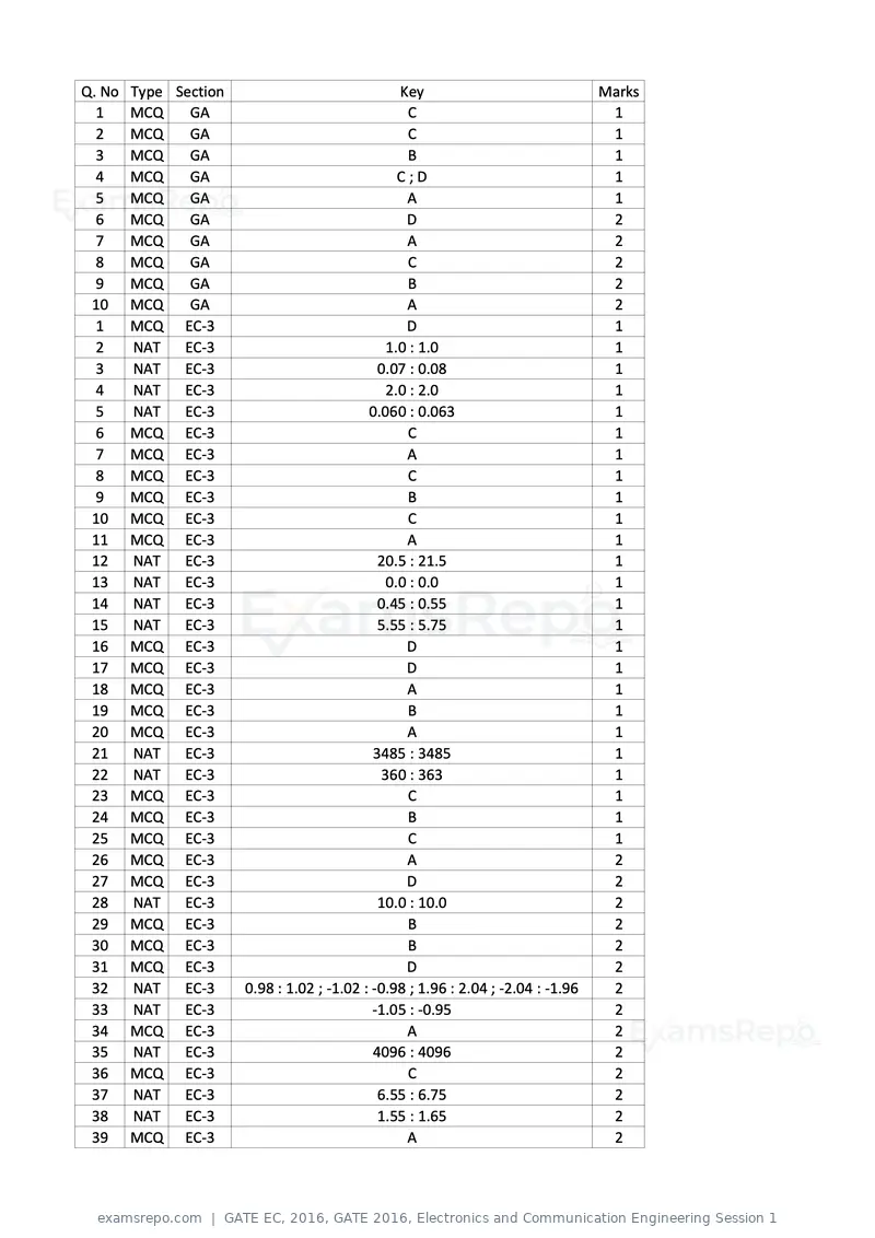
Text of page 63
Q. No Type Section                              Key                              Marks
  1   MCQ    GA                                  C                                1
  2   MCQ    GA                                  C                                1
  3   MCQ    GA                                  B                                1
  4   MCQ    GA                                 C;D                               1
  5   MCQ    GA                                  A                                1
  6   MCQ    GA                                  D                                2
  7   MCQ    GA                                  A                                2
  8   MCQ    GA                                  C                                2
  9   MCQ    GA                                  B                                2
 10 MCQ      GA                                  A                                2
  1   MCQ EC-3                                   D                                1
  2   NAT   EC-3                              1.0 : 1.0                           1
  3   NAT   EC-3                            0.07 : 0.08                           1
  4   NAT   EC-3                              2.0 : 2.0                           1
  5   NAT   EC-3                          0.060 : 0.063                           1
  6   MCQ EC-3                                   C                                1
  7   MCQ EC-3                                   A                                1
  8   MCQ EC-3                                   C                                1
  9   MCQ EC-3                                   B                                1
 10 MCQ EC-3                                     C                                1
 11 MCQ EC-3                                     A                                1
 12   NAT   EC-3                            20.5 : 21.5                           1
 13   NAT   EC-3                              0.0 : 0.0                           1
 14   NAT   EC-3                            0.45 : 0.55                           1
 15   NAT   EC-3                            5.55 : 5.75                           1
 16 MCQ EC-3                                     D                                1
 17 MCQ EC-3                                     D                                1
 18 MCQ EC-3                                     A                                1
 19 MCQ EC-3                                     B                                1
 20 MCQ EC-3                                     A                                1
 21   NAT   EC-3                           3485 : 3485                            1
 22   NAT   EC-3                             360 : 363                            1
 23 MCQ EC-3                                     C                                1
 24 MCQ EC-3                                     B                                1
 25 MCQ EC-3                                     C                                1
 26 MCQ EC-3                                     A                                2
 27 MCQ EC-3                                     D                                2
 28   NAT   EC-3                            10.0 : 10.0                           2
 29 MCQ EC-3                                     B                                2
 30 MCQ EC-3                                     B                                2
 31 MCQ EC-3                                     D                                2
 32   NAT   EC-3     0.98 : 1.02 ; -1.02 : -0.98 ; 1.96 : 2.04 ; -2.04 : -1.96    2
 33   NAT   EC-3                           -1.05 : -0.95                          2
 34 MCQ EC-3                                     A                                2
 35   NAT   EC-3                           4096 : 4096                            2
 36 MCQ EC-3                                     C                                2
 37   NAT   EC-3                            6.55 : 6.75                           2
 38   NAT   EC-3                            1.55 : 1.65                           2
 39 MCQ EC-3                                     A                                2
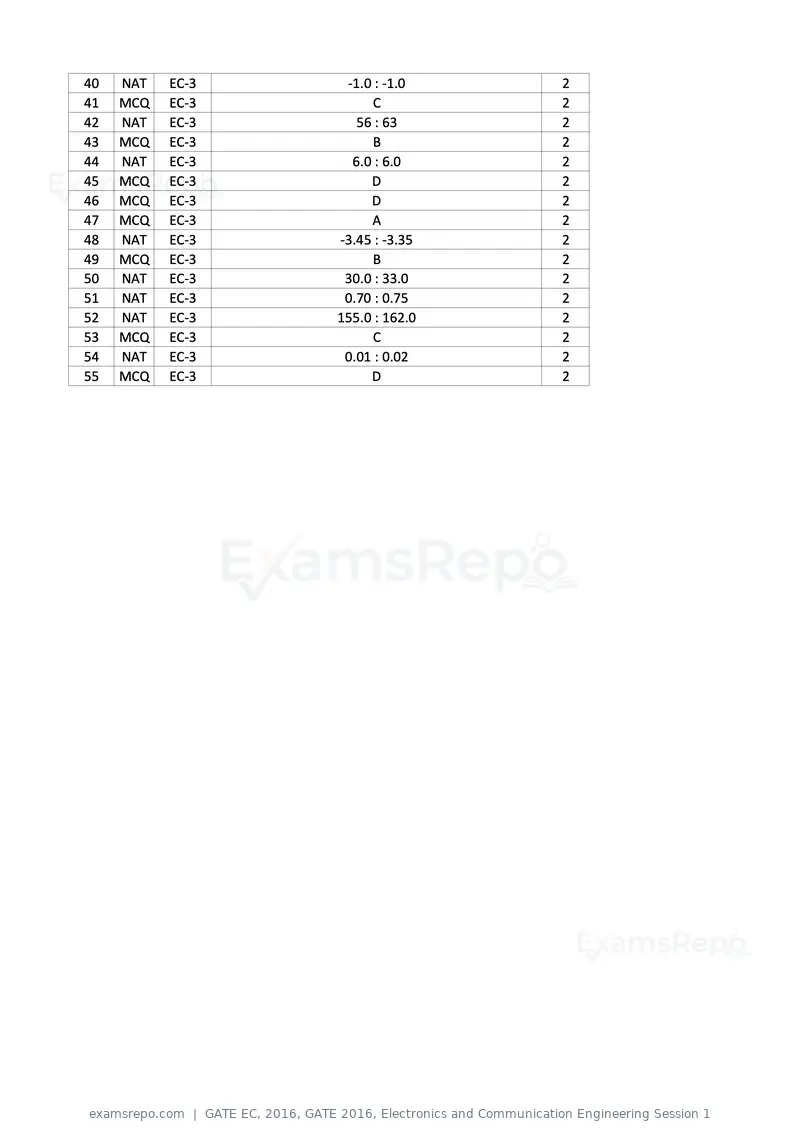
Text of page 64
40   NAT   EC-3    -1.0 : -1.0    2
41   MCQ   EC-3        C          2
42   NAT   EC-3      56 : 63      2
43   MCQ   EC-3        B          2
44   NAT   EC-3     6.0 : 6.0     2
45   MCQ   EC-3        D          2
46   MCQ   EC-3        D          2
47   MCQ   EC-3        A          2
48   NAT   EC-3   -3.45 : -3.35   2
49   MCQ   EC-3        B          2
50   NAT   EC-3    30.0 : 33.0    2
51   NAT   EC-3    0.70 : 0.75    2
52   NAT   EC-3   155.0 : 162.0   2
53   MCQ   EC-3        C          2
54   NAT   EC-3    0.01 : 0.02    2
55   MCQ   EC-3        D          2
Official key not published for this paper.
Page 1 of 64
Source: GATE. Question paper published by GATE.