
GATE EC 2018: Electronics and Communication Engineering

Text of page 1
GATE 2018                                                                    General Aptitude (GA) Set-5

Q. 1 – Q. 5 carry one mark each.
 Q.1   “By giving him the last ______ of the cake, you will ensure lasting _____ in our house
       today.”

       The words that best fill the blanks in the above sentence are

       (A) peas, piece                                    (B) piece, peace
       (C) peace, piece                                   (D) peace, peas


 Q.2   “Even though there is a vast scope for its ________, tourism has remained a/an _________
       area.”

       The words that best fill the blanks in the above sentence are

       (A) improvement, neglected
       (B) rejection, approved
       (C) fame, glum
       (D) interest, disinterested


 Q.3   If the number 715∎423 is divisible by 3 (∎ denotes the missing digit in the thousandths
       place), then the smallest whole number in the place of ∎ is _________.

       (A) 0                 (B) 2                        (C) 5                 (D) 6


 Q.4                               1   1        1        1
       What is the value of 1 + +           +        +         + ⋯?
                                   4   16       64       256


       (A) 2                       7                            3                     4
                             (B)                          (C)                   (D)
                                   4                            2                     3


 Q.5   A 1.5 m tall person is standing at a distance of 3 m from a lamp post. The light from the
       lamp at the top of the post casts her shadow. The length of the shadow is twice her height.
       What is the height of the lamp post in meters?

       (A) 1.5               (B) 3                        (C) 4.5               (D) 6


Q. 6 – Q. 10 carry two marks each.

 Q.6   Leila aspires to buy a car worth Rs. 10,00,000 after 5 years. What is the minimum amount
       in Rupees that she should deposit now in a bank which offers 10% annual rate of interest, if
       the interest was compounded annually?

       (A) 5,00,000                                       (B) 6,21,000
       (C) 6,66,667                                       (D) 7,50,000
GA                                                                                                    1/3
Text of page 2
GATE 2018                                                            General Aptitude (GA) Set-5

Q.7   Two alloys A and B contain gold and copper in the ratios of 2:3 and 3:7 by mass,
      respectively. Equal masses of alloys A and B are melted to make an alloy C. The ratio of
      gold to copper in alloy C is ______.

      (A) 5:10                  (B) 7:13           (C) 6:11              (D) 9:13


Q.8   The Cricket Board has long recognized John’s potential as a leader of the team. However,
      his on-field temper has always been a matter of concern for them since his junior days.
      While this aggression has filled stadia with die-hard fans, it has taken a toll on his own
      batting. Until recently, it appeared that he found it difficult to convert his aggression into
      big scores. Over the past three seasons though, that picture of John has been replaced by a
      cerebral, calculative and successful batsman-captain. After many years, it appears that the
      team has finally found a complete captain.

      Which of the following statements can be logically inferred from the above paragraph?
        (i) Even as a junior cricketer, John was considered a good captain.
       (ii) Finding a complete captain is a challenge.
      (iii) Fans and the Cricket Board have differing views on what they want in a captain.
      (iv) Over the past three seasons John has accumulated big scores.

      (A) (i), (ii) and (iii) only
      (B) (iii) and (iv) only
      (C) (ii) and (iv) only
      (D) (i), (ii), (iii) and (iv)


Q.9   A cab was involved in a hit and run accident at night. You are given the following data
      about the cabs in the city and the accident.
        (i) 85% of cabs in the city are green and the remaining cabs are blue.
       (ii) A witness identified the cab involved in the accident as blue.
      (iii) It is known that a witness can correctly identify the cab colour only 80% of the
              time.

      Which of the following options is closest to the probability that the accident was caused by
      a blue cab?

      (A) 12%                   (B) 15%            (C) 41%               (D) 80%


GA                                                                                                   2/3
Text of page 3
GATE 2018                                                           General Aptitude (GA) Set-5
 Q.10 A coastal region with unparalleled beauty is home to many species of animals. It is dotted
      with coral reefs and unspoilt white sandy beaches. It has remained inaccessible to tourists
      due to poor connectivity and lack of accommodation. A company has spotted the
      opportunity and is planning to develop a luxury resort with helicopter service to the nearest
      major city airport. Environmentalists are upset that this would lead to the region becoming
      crowded and polluted like any other major beach resorts.

        Which one of the following statements can be logically inferred from the information given
        in the above paragraph?

        (A) The culture and tradition of the local people will be influenced by the tourists.
        (B) The region will become crowded and polluted due to tourism.
        (C) The coral reefs are on the decline and could soon vanish.
        (D) Helicopter connectivity would lead to an increase in tourists coming to the region.


                            END OF THE QUESTION PAPER


GA                                                                                                3/3
Text of page 4
GATE 2018                                                                   Electronics and Communication Engineering


Q. 1 – Q. 25 carry one mark each.
     Q.1    Two identical nMOS transistors M1 and M2 are connected as shown below. The circuit is
            used as an amplifier with the input connected between G and S terminals and the output taken
            between D and S terminals. Vbias and VD are so adjusted that both transistors are in saturation.
                                                                                      ∂iD
            The transconductance of this combination is defined as gm =                       while the output
                                                                                     ∂vGS
                                 ∂vDS
            resistance is ro =          , where iD is the current flowing into the drain of M2 . Let gm1 ,
                                  ∂iD
            gm2 be the transconductances and ro1 , ro2 be the output resistances of transistors M1 and
            M2 , respectively.


            Which of the following statements about estimates for gm and ro is correct?
            (A) gm ≈ gm1 . gm2 . ro2 and ro ≈ ro1 + ro2 .
            (B) gm ≈ gm1 + gm2 and ro ≈ ro1 + ro2 .
            (C) gm ≈ gm1 and ro ≈ ro1 . gm2 . ro2.
            (D) gm ≈ gm1 and ro ≈ ro2 .

     Q.2    In the circuit shown below, the op-amp is ideal and Zener voltage of the diode is 2.5 volts.
            At the input, unit step voltage is applied, i.e. vIN (t) = u(t) volts. Also, at t = 0, the
            voltage across each of the capacitors is zero.


            The time t, in milliseconds, at which the output voltage vOUT crosses −10 V is
            (A) 2.5                (B) 5                  (C) 7.5                 (D) 10

     Q.3    A good transimpedance amplifier has
            (A) low input impedance and high output impedance.
            (B) high input impedance and high output impedance.
            (C) high input impedance and low output impedance.
            (D) low input impedance and low output impedance.


EC                                                                                                               1/17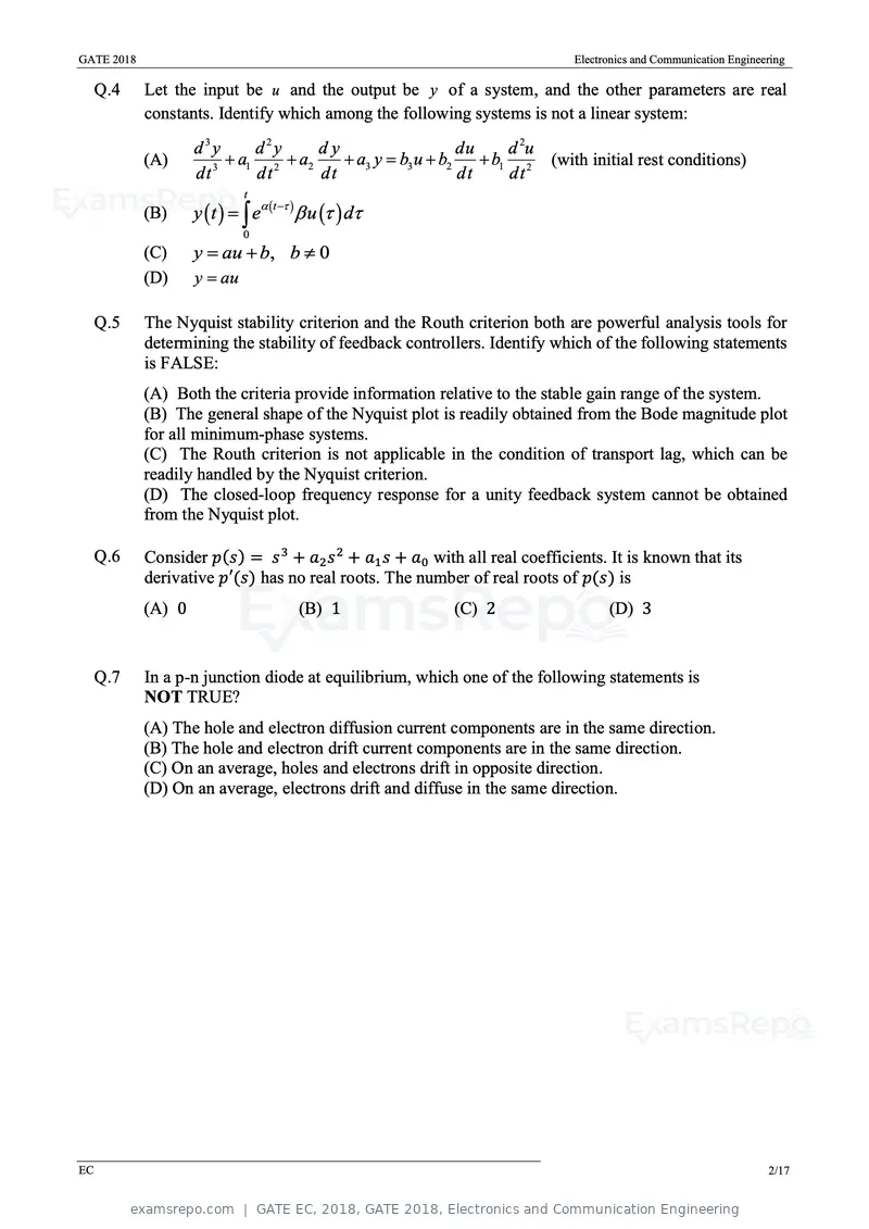
Text of page 5
GATE 2018 Electronics and Communication Engineering
Q.4 Let the input be u and the output be y of a system, and the other parameters are real
constants. Identify which among the following systems is not a linear system:
d3y d2y dy du d 2u
(A) a1 2 a2 a3 y b3 u b2 b1 2 (with initial rest conditions)
dt 3 dt dt dt dt
t
y t e t u d
(B)
0
(C) y au b, b 0
(D) y au
Q.5 The Nyquist stability criterion and the Routh criterion both are powerful analysis tools for
determining the stability of feedback controllers. Identify which of the following statements
is FALSE:
(A) Both the criteria provide information relative to the stable gain range of the system.
(B) The general shape of the Nyquist plot is readily obtained from the Bode magnitude plot
for all minimum-phase systems.
(C) The Routh criterion is not applicable in the condition of transport lag, which can be
readily handled by the Nyquist criterion.
(D) The closed-loop frequency response for a unity feedback system cannot be obtained
from the Nyquist plot.
Q.6 Consider p(s) = s 3 + a2 s 2 + a1 s + a0 with all real coefficients. It is known that its
derivative p′(s) has no real roots. The number of real roots of p(s) is
(A) 0 (B) 1 (C) 2 (D) 3
Q.7 In a p-n junction diode at equilibrium, which one of the following statements is
NOT TRUE?
(A) The hole and electron diffusion current components are in the same direction.
(B) The hole and electron drift current components are in the same direction.
(C) On an average, holes and electrons drift in opposite direction.
(D) On an average, electrons drift and diffuse in the same direction.
EC 2/17
Text of page 6
GATE 2018                                                                         Electronics and Communication Engineering

     Q.8    The logic function f ( X , Y ) realized by the given circuit is

                                                           VDD


                              X                                                           X

                              Y                                                           Y
                                                                     f (X , Y )


            (A) NOR                 (B) AND                 (C) NAND                    (D) XOR

     Q.9    A function F(A, B, C) defined by three Boolean variables A, B and C when expressed as sum
            of products is given by
                                         F = A̅ ⋅ B̅ ⋅ C̅ + A̅ ⋅ B ⋅ C̅ + A ⋅ B̅ ⋅ C̅
                     ̅ ̅       ̅
            where, A, B , and C are the complements of the respective variables. The product of sums
            (POS) form of the function F is

            (A) F = (A + B + C) ⋅ (A + B̅ + C) ⋅ (A̅ + B + C)
            (B) F = (A̅ + B̅ + C̅ ) ⋅ (A̅ + B + C̅ ) ⋅ (A + B̅ + C̅ )
            (C) F = (A + B + C̅ ) ⋅ (A + B̅ + C̅ ) ⋅ (A̅ + B + C̅ ) ⋅ (A̅ + B̅ + C) ⋅ (A̅ + B̅ + C̅ )
            (D) F = (A̅ + B̅ + C) ⋅ (A̅ + B + C) ⋅ (A + B̅ + C) ⋅ (A + B + C̅ ) ⋅ (A + B + C)


EC                                                                                                                     3/17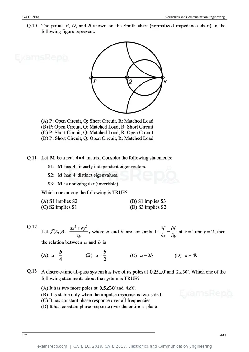
Text of page 7
GATE 2018 Electronics and Communication Engineering
Q.10 The points P, Q, and R shown on the Smith chart (normalized impedance chart) in the
following figure represent:
P Q R
(A) P: Open Circuit, Q: Short Circuit, R: Matched Load
(B) P: Open Circuit, Q: Matched Load, R: Short Circuit
(C) P: Short Circuit, Q: Matched Load, R: Open Circuit
(D) P: Short Circuit, Q: Open Circuit, R: Matched Load
Q.11 Let M be a real 4 4 matrix. Consider the following statements:
S1: M has 4 linearly independent eigenvectors.
S2: M has 4 distinct eigenvalues.
S3: M is non-singular (invertible).
Which one among the following is TRUE?
(A) S1 implies S2 (B) S1 implies S3
(C) S2 implies S1 (D) S3 implies S2
Q.12 ax 2 by 2 f f
Let f ( x, y ) , where a and b are constants. If at x 1 and y 2 , then
xy x y
the relation between a and b is
b b
(A) a (B) a (C) a 2b (D) a 4b
4 2
Q.13 A discrete-time all-pass system has two of its poles at 0.250 and 230 . Which one of the
following statements about the system is TRUE?
(A) It has two more poles at 0.530 and 40 .
(B) It is stable only when the impulse response is two-sided.
(C) It has constant phase response over all frequencies.
(D) It has constant phase response over the entire z-plane.
EC 4/17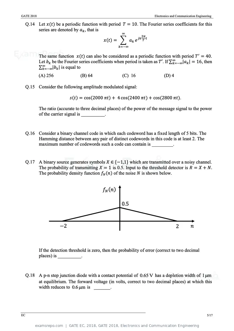
Text of page 8
GATE 2018                                                                   Electronics and Communication Engineering

     Q.14 Let x(t) be a periodic function with period T = 10. The Fourier series coefficients for this
          series are denoted by ak , that is
                                                         ∞
                                                                    2π
                                               x(t) = ∑ ak e jk T t
                                                        k=−∞

            The same function x(t) can also be considered as a periodic function with period T ′ = 40.
            Let bk be the Fourier series coefficients when period is taken as T′. If ∑∞
                                                                                      k=−∞|ak | = 16, then
             ∞
            ∑k=−∞|bk | is equal to
            (A) 256                (B) 64                 (C) 16                  (D) 4

     Q.15 Consider the following amplitude modulated signal:

                             s(t) = cos(2000 πt) + 4 cos(2400 πt) + cos(2800 πt).

            The ratio (accurate to three decimal places) of the power of the message signal to the power
            of the carrier signal is __________.


     Q.16 Consider a binary channel code in which each codeword has a fixed length of 5 bits. The
          Hamming distance between any pair of distinct codewords in this code is at least 2. The
          maximum number of codewords such a code can contain is _________.


     Q.17 A binary source generates symbols X ∈ {−1,1} which are transmitted over a noisy channel.
          The probability of transmitting X = 1 is 0.5. Input to the threshold detector is R = X + N.
          The probability density function fN (n) of the noise N is shown below.


                                               fN (n)

                                                         0.5


                       −2                                                                  2         n


            If the detection threshold is zero, then the probability of error (correct to two decimal
            places) is __________.


     Q.18 A p-n step junction diode with a contact potential of 0.65 V has a depletion width of 1μm
          at equilibrium. The forward voltage (in volts, correct to two decimal places) at which this
          width reduces to 0.6 μm is _______.


EC                                                                                                               5/17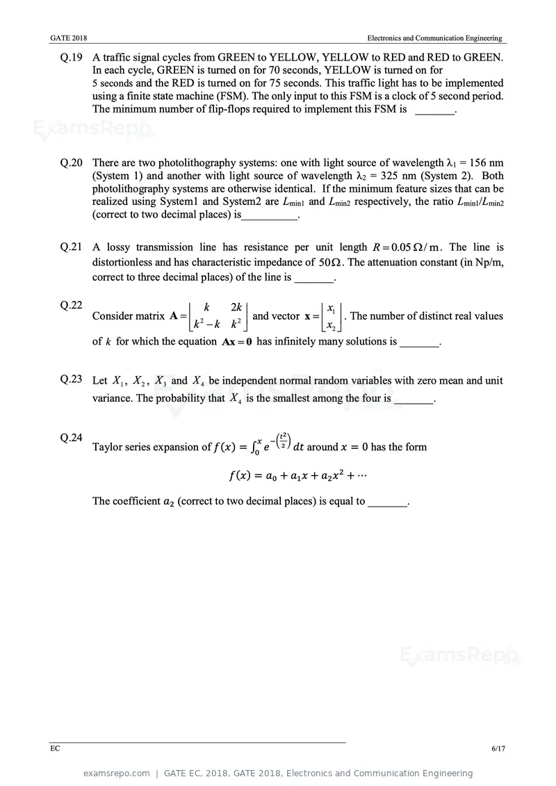
Text of page 9
GATE 2018 Electronics and Communication Engineering
Q.19 A traffic signal cycles from GREEN to YELLOW, YELLOW to RED and RED to GREEN.
In each cycle, GREEN is turned on for 70 seconds, YELLOW is turned on for
5 seconds and the RED is turned on for 75 seconds. This traffic light has to be implemented
using a finite state machine (FSM). The only input to this FSM is a clock of 5 second period.
The minimum number of flip-flops required to implement this FSM is _______.
Q.20 There are two photolithography systems: one with light source of wavelength λ1 = 156 nm
(System 1) and another with light source of wavelength λ2 = 325 nm (System 2). Both
photolithography systems are otherwise identical. If the minimum feature sizes that can be
realized using System1 and System2 are Lmin1 and Lmin2 respectively, the ratio Lmin1/Lmin2
(correct to two decimal places) is__________.
Q.21 A lossy transmission line has resistance per unit length R 0.05 / m . The line is
distortionless and has characteristic impedance of 50 . The attenuation constant (in Np/m,
correct to three decimal places) of the line is _______.
Q.22 k 2k x
Consider matrix A 2 2
and vector x 1 . The number of distinct real values
k k k x2
of k for which the equation Ax 0 has infinitely many solutions is _______.
Q.23 Let X 1 , X 2 , X 3 and X 4 be independent normal random variables with zero mean and unit
variance. The probability that X 4 is the smallest among the four is _______.
Q.24 t2
x −( )
Taylor series expansion of f(x) = ∫0 e 2 dt around x = 0 has the form
f(x) = a0 + a1 x + a2 x 2 + ⋯
The coefficient a2 (correct to two decimal places) is equal to _______.
EC 6/17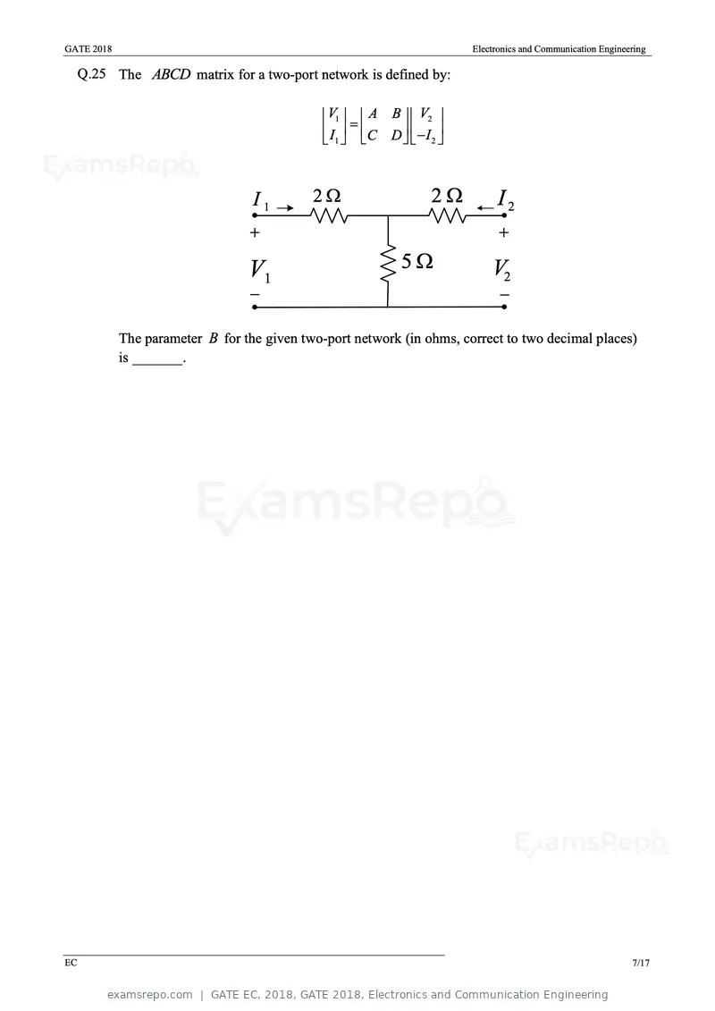
Text of page 10
GATE 2018 Electronics and Communication Engineering
Q.25 The ABCD matrix for a two-port network is defined by:
V1 A B V2
I C D I
1 2
I1 2 2 I2
V1 5 V2
The parameter B for the given two-port network (in ohms, correct to two decimal places)
is _______.
EC 7/17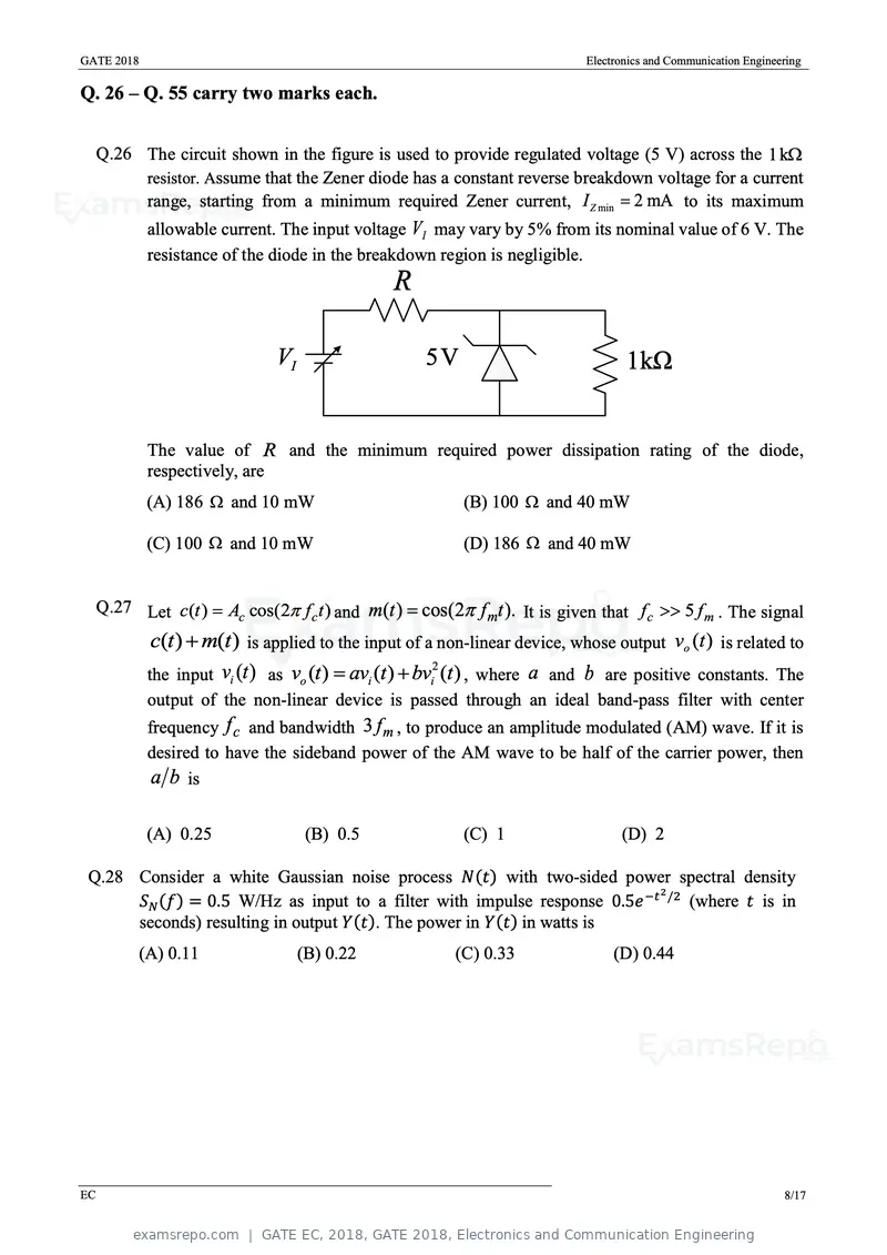
Text of page 11
GATE 2018 Electronics and Communication Engineering
Q. 26 – Q. 55 carry two marks each.
Q.26 The circuit shown in the figure is used to provide regulated voltage (5 V) across the 1k
resistor. Assume that the Zener diode has a constant reverse breakdown voltage for a current
range, starting from a minimum required Zener current, I Z min 2 mA to its maximum
allowable current. The input voltage VI may vary by 5% from its nominal value of 6 V. The
resistance of the diode in the breakdown region is negligible.
R
VI 5V 1kΩ
The value of R and the minimum required power dissipation rating of the diode,
respectively, are
(A) 186 and 10 mW (B) 100 and 40 mW
(C) 100 and 10 mW (D) 186 and 40 mW
Q.27 Let c(t ) Ac cos(2 f c t ) and m(t ) cos(2 f mt ). It is given that f c 5 f m . The signal
c(t ) m(t ) is applied to the input of a non-linear device, whose output vo (t ) is related to
the input vi (t ) as vo (t ) avi (t ) bvi (t ) , where a and b are positive constants. The
2
output of the non-linear device is passed through an ideal band-pass filter with center
frequency f c and bandwidth 3 f m , to produce an amplitude modulated (AM) wave. If it is
desired to have the sideband power of the AM wave to be half of the carrier power, then
a b is
(A) 0.25 (B) 0.5 (C) 1 (D) 2
Q.28 Consider a white Gaussian noise process N(t) with two-sided power spectral density
2
SN (f) = 0.5 W/Hz as input to a filter with impulse response 0.5e −t /2 (where t is in
seconds) resulting in output Y(t). The power in Y(t) in watts is
(A) 0.11 (B) 0.22 (C) 0.33 (D) 0.44
EC 8/17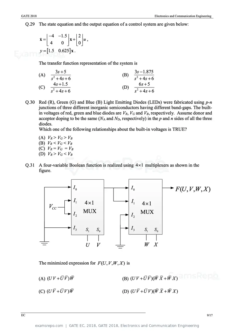
Text of page 12
GATE 2018 Electronics and Communication Engineering
Q.29 The state equation and the output equation of a control system are given below:
4 1.5 2
x x u ,
4 0 0
y 1.5 0.625 x .
The transfer function representation of the system is
3s 5 3s 1.875
(A) (B)
s 4s 6
2
s 2 4s 6
4s 1.5 6s 5
(C) (D)
s 4s 6
2
s 4s 6
2
Q.30 Red (R), Green (G) and Blue (B) Light Emitting Diodes (LEDs) were fabricated using p-n
junctions of three different inorganic semiconductors having different band-gaps. The built-
in voltages of red, green and blue diodes are VR, VG and VB, respectively. Assume donor and
acceptor doping to be the same (NA and ND, respectively) in the p and n sides of all the three
diodes.
Which one of the following relationships about the built-in voltages is TRUE?
(A) VR > VG > VB
(B) VR < VG < VB
(C) VR = VG = VB
(D) VR > VG < VB
Q.31 A four-variable Boolean function is realized using 4 1 multiplexers as shown in the
figure.
I0 I0 F (U , V ,W , X )
I1 4 1 I1
VCC 4 1
I2 MUX MUX
I2
I3 S1 S0 I3 S1 S0
U V W X
The minimized expression for F (U , V ,W , X ) is
(A) (U V U V ) W (B) (U V U V )(W X W X )
(C) (U V U V ) W (D) (U V U V )(W X W X )
EC 9/17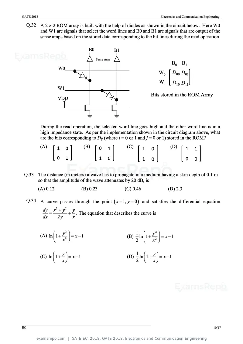
Text of page 13
GATE 2018 Electronics and Communication Engineering
Q.32 A 2 2 ROM array is built with the help of diodes as shown in the circuit below. Here W0
and W1 are signals that select the word lines and B0 and B1 are signals that are output of the
sense amps based on the stored data corresponding to the bit lines during the read operation.
B0 B1
Sense amps
B0 B1
W0
W0 D00 D01
W1 D10 D11
W1
Bits stored in the ROM Array
VDD
During the read operation, the selected word line goes high and the other word line is in a
high impedance state. As per the implementation shown in the circuit diagram above, what
are the bits corresponding to Dij (where i = 0 or 1 and j = 0 or 1) stored in the ROM?
(A) 1 0 (B) 0 1 (C) 1 0 (D) 1 1
0 1 1 0 1 0 0 0
Q.33 The distance (in meters) a wave has to propagate in a medium having a skin depth of 0.1 m
so that the amplitude of the wave attenuates by 20 dB, is
(A) 0.12 (B) 0.23 (C) 0.46 (D) 2.3
Q.34 A curve passes through the point x 1, y 0 and satisfies the differential equation
dy x 2 y 2 y
. The equation that describes the curve is
dx 2y x
2
1 y2
(A) ln 1 y2 x 1 (B) ln 1 x 1
x 2 x2
y 1 y
(C) ln 1 x 1 (D) ln 1 x 1
x 2 x
EC 10/17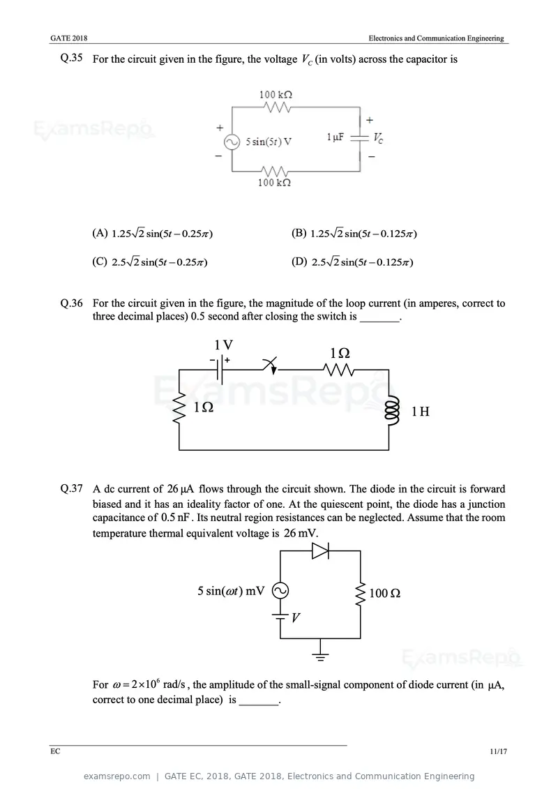
Text of page 14
GATE 2018 Electronics and Communication Engineering
Q.35 For the circuit given in the figure, the voltage VC (in volts) across the capacitor is
(A) 1.25 2 sin(5t 0.25 ) (B) 1.25 2 sin(5t 0.125 )
(C) 2.5 2 sin(5t 0.25 ) (D) 2.5 2 sin(5t 0.125 )
Q.36 For the circuit given in the figure, the magnitude of the loop current (in amperes, correct to
three decimal places) 0.5 second after closing the switch is _______.
1V
1
1 1H
Q.37 A dc current of 26 μA flows through the circuit shown. The diode in the circuit is forward
biased and it has an ideality factor of one. At the quiescent point, the diode has a junction
capacitance of 0.5 nF . Its neutral region resistances can be neglected. Assume that the room
temperature thermal equivalent voltage is 26 mV.
5 sin( t ) mV 100
V
For 2 106 rad/s , the amplitude of the small-signal component of diode current (in μA,
correct to one decimal place) is _______.
EC 11/17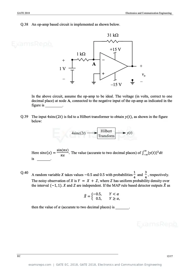
Text of page 15
GATE 2018 Electronics and Communication Engineering
Q.38 An op-amp based circuit is implemented as shown below.
31 k
+15 V
1 k
+ –
A +
1V
+ vo
–
–
–15 V
In the above circuit, assume the op-amp to be ideal. The voltage (in volts, correct to one
decimal place) at node A, connected to the negative input of the op-amp as indicated in the
figure is _________.
Q.39 The input 4sinc(2t) is fed to a Hilbert transformer to obtain y(t), as shown in the figure
below:
sin(πx) ∞
Here sinc(x) = . The value (accurate to two decimal places) of ∫−∞|y(t)|2 dt
πx
is _______.
Q.40 1 3
A random variable X takes values −0.5 and 0.5 with probabilities and , respectively.
4 4
The noisy observation of X is Y = X + Z, where Z has uniform probability density over
the interval (−1, 1). X and Z are independent. If the MAP rule based detector outputs X̂ as
−0.5, Y<α
X̂ = {
0.5, Y ≥ α,
then the value of α (accurate to two decimal places) is _______.
EC 12/17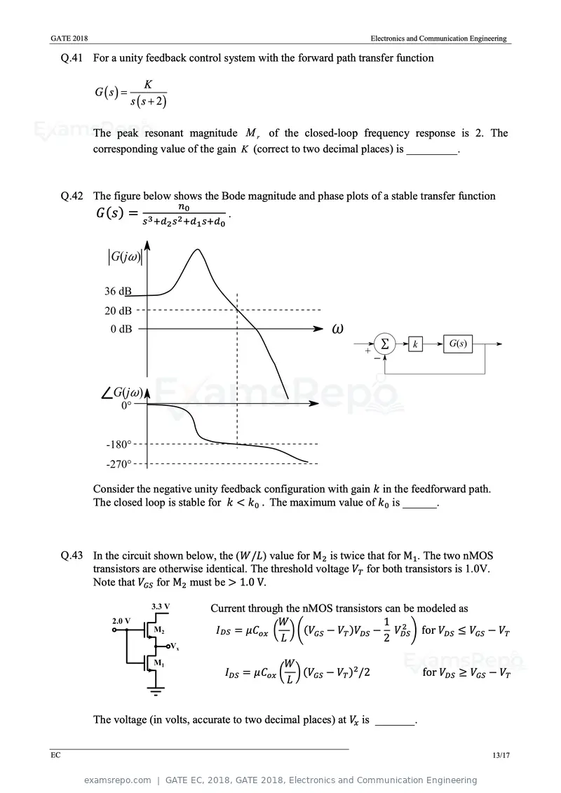
Text of page 16
GATE 2018 Electronics and Communication Engineering
Q.41 For a unity feedback control system with the forward path transfer function
K
G s
s s 2
The peak resonant magnitude M r of the closed-loop frequency response is 2. The
corresponding value of the gain K (correct to two decimal places) is _________.
Q.42 The figure below shows the Bode magnitude and phase plots of a stable transfer function
n0
G (s ) = 3 2 .
s +d2 s +d1 s+d0
Consider the negative unity feedback configuration with gain k in the feedforward path.
The closed loop is stable for k < k0 . The maximum value of k0 is ______.
Q.43 In the circuit shown below, the (W/L) value for M2 is twice that for M1. The two nMOS
transistors are otherwise identical. The threshold voltage VT for both transistors is 1.0V.
Note that VGS for M2 must be > 1.0 V.
Current through the nMOS transistors can be modeled as
W 1 2
IDS = μCox ( ) ((VGS − VT )VDS − VDS ) for VDS ≤ VGS − VT
L 2
W
IDS = μCox ( ) (VGS − VT )2 /2 for VDS ≥ VGS − VT
L
The voltage (in volts, accurate to two decimal places) at Vx is _______.
EC 13/17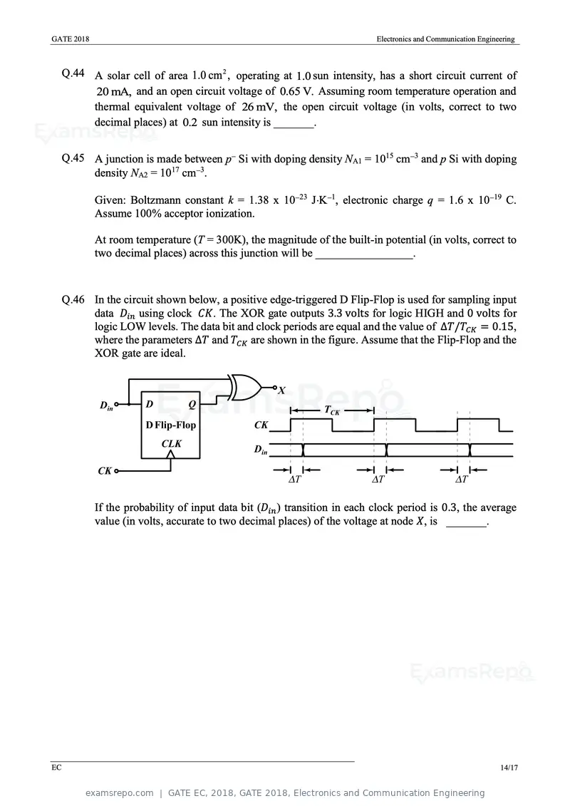
Text of page 17
GATE 2018 Electronics and Communication Engineering
Q.44 A solar cell of area 1.0 cm 2 , operating at 1.0 sun intensity, has a short circuit current of
20 mA, and an open circuit voltage of 0.65 V. Assuming room temperature operation and
thermal equivalent voltage of 26 mV, the open circuit voltage (in volts, correct to two
decimal places) at 0.2 sun intensity is _______.
Q.45 A junction is made between p Si with doping density NA1 = 1015 cm3 and p Si with doping
density NA2 = 1017 cm3.
Given: Boltzmann constant k = 1.38 x 10²³ JK1, electronic charge q = 1.6 x 10¹⁹ C.
Assume 100% acceptor ionization.
At room temperature (T = 300K), the magnitude of the built-in potential (in volts, correct to
two decimal places) across this junction will be _________________.
Q.46 In the circuit shown below, a positive edge-triggered D Flip-Flop is used for sampling input
data Din using clock CK. The XOR gate outputs 3.3 volts for logic HIGH and 0 volts for
logic LOW levels. The data bit and clock periods are equal and the value of ΔT/TCK = 0.15,
where the parameters ΔT and TCK are shown in the figure. Assume that the Flip-Flop and the
XOR gate are ideal.
If the probability of input data bit (Din ) transition in each clock period is 0.3, the average
value (in volts, accurate to two decimal places) of the voltage at node X, is _______.
EC 14/17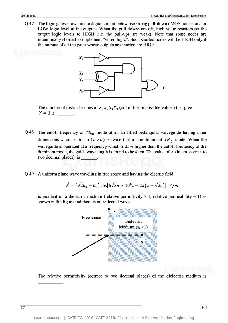
Text of page 18
GATE 2018 Electronics and Communication Engineering
Q.47 The logic gates shown in the digital circuit below use strong pull-down nMOS transistors for
LOW logic level at the outputs. When the pull-downs are off, high-value resistors set the
output logic levels to HIGH (i.e. the pull-ups are weak). Note that some nodes are
intentionally shorted to implement “wired logic”. Such shorted nodes will be HIGH only if
the outputs of all the gates whose outputs are shorted are HIGH.
The number of distinct values of X3 X2 X1 X0 (out of the 16 possible values) that give
Y = 1 is _______.
Q.48 The cutoff frequency of TE01 mode of an air filled rectangular waveguide having inner
dimensions a cm b cm ( a b ) is twice that of the dominant TE10 mode. When the
waveguide is operated at a frequency which is 25% higher than the cutoff frequency of the
dominant mode, the guide wavelength is found to be 4 cm. The value of b (in cm, correct to
two decimal places) is _______.
Q.49 A uniform plane wave traveling in free space and having the electric field
⃗E = (√2âx − âz ) cos[6√3π × 108 t − 2π(x + √2z)] V/m
is incident on a dielectric medium (relative permittivity > 1, relative permeability = 1) as
shown in the figure and there is no reflected wave.
z
Free space
Dielectric
Medium (r >1)
x
The relative permittivity (correct to two decimal places) of the dielectric medium is
___________.
EC 15/17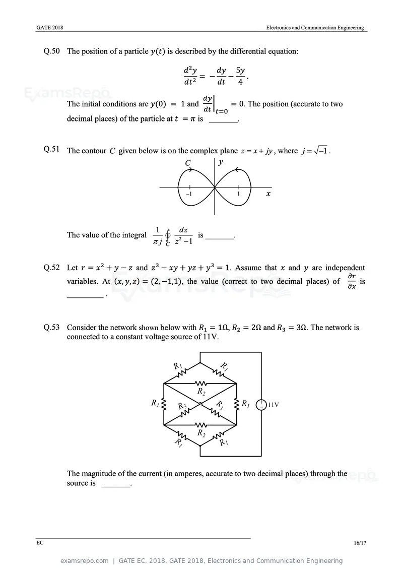
Text of page 19
GATE 2018 Electronics and Communication Engineering
Q.50 The position of a particle y(t) is described by the differential equation:
d2y dy 5y
= − − .
dt 2 dt 4
dy
The initial conditions are y(0) = 1 and | = 0. The position (accurate to two
dt t=0
decimal places) of the particle at t = π is _______.
Q.51 The contour C given below is on the complex plane z x jy , where j 1 .
C y
1 1 x
1 dz
j C z 1
The value of the integral 2
is _______.
Q.52 Let r = x 2 + y − z and z 3 − xy + yz + y 3 = 1. Assume that x and y are independent
∂r
variables. At (x, y, z) = (2, −1,1), the value (correct to two decimal places) of is
∂x
_________ .
Q.53 Consider the network shown below with R1 = 1Ω, R2 = 2Ω and R3 = 3Ω. The network is
connected to a constant voltage source of 11V.
The magnitude of the current (in amperes, accurate to two decimal places) through the
source is _______.
EC 16/17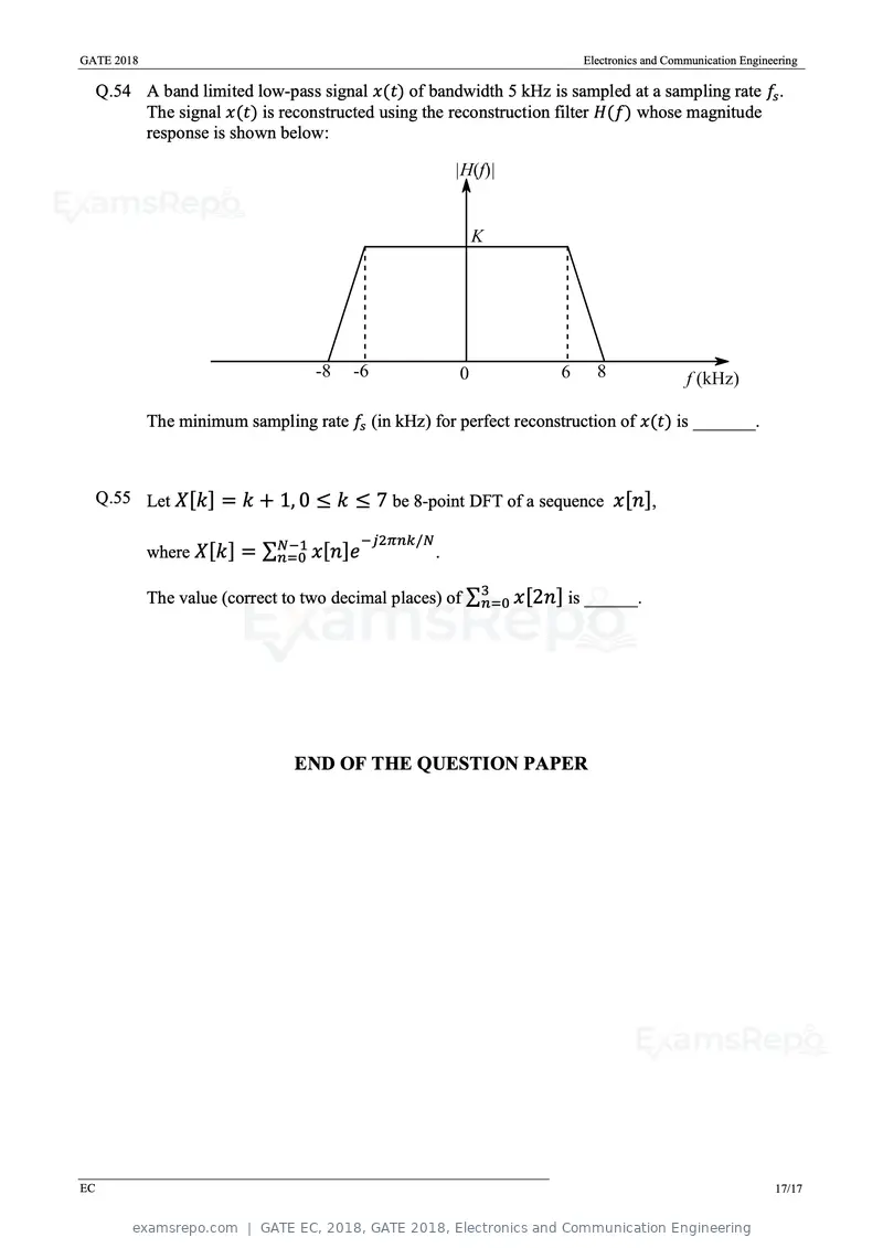
Text of page 20
GATE 2018                                                              Electronics and Communication Engineering

     Q.54 A band limited low-pass signal x(t) of bandwidth 5 kHz is sampled at a sampling rate fs .
          The signal x(t) is reconstructed using the reconstruction filter H(f) whose magnitude
          response is shown below:


            The minimum sampling rate fs (in kHz) for perfect reconstruction of x(t) is _______.


     Q.55 Let X[k] = k + 1, 0 ≤ k ≤ 7 be 8-point DFT of a sequence x[n],

                                         −j2πnk/N
            where X[k] = ∑N−1
                          n=0 x[n]e                 .

            The value (correct to two decimal places) of ∑3n=0 x[2n] is ______.


                                END OF THE QUESTION PAPER


EC                                                                                                         17/17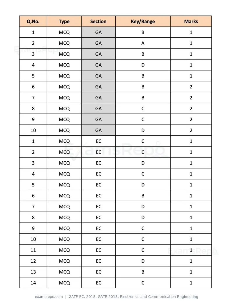
Text of page 21
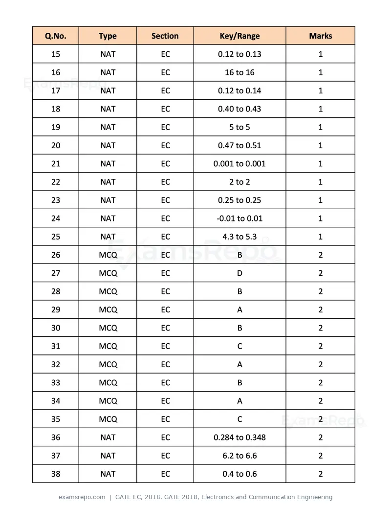
Q.No.   Type   Section   Key/Range   Marks

 1      MCQ      GA         B          1

 2      MCQ      GA         A          1

 3      MCQ      GA         B          1

 4      MCQ      GA         D          1

 5      MCQ      GA         B          1

 6      MCQ      GA         B          2

 7      MCQ      GA         B          2

 8      MCQ      GA         C          2

 9      MCQ      GA         C          2

 10     MCQ      GA         D          2

 1      MCQ      EC         C          1

 2      MCQ      EC         C          1

 3      MCQ      EC         D          1

 4      MCQ      EC         C          1

 5      MCQ      EC         D          1

 6      MCQ      EC         B          1

 7      MCQ      EC         D          1

 8      MCQ      EC         D          1

 9      MCQ      EC         C          1

 10     MCQ      EC         C          1

 11     MCQ      EC         C          1

 12     MCQ      EC         D          1

 13     MCQ      EC         B          1

 14     MCQ      EC         C          1
Text of page 22
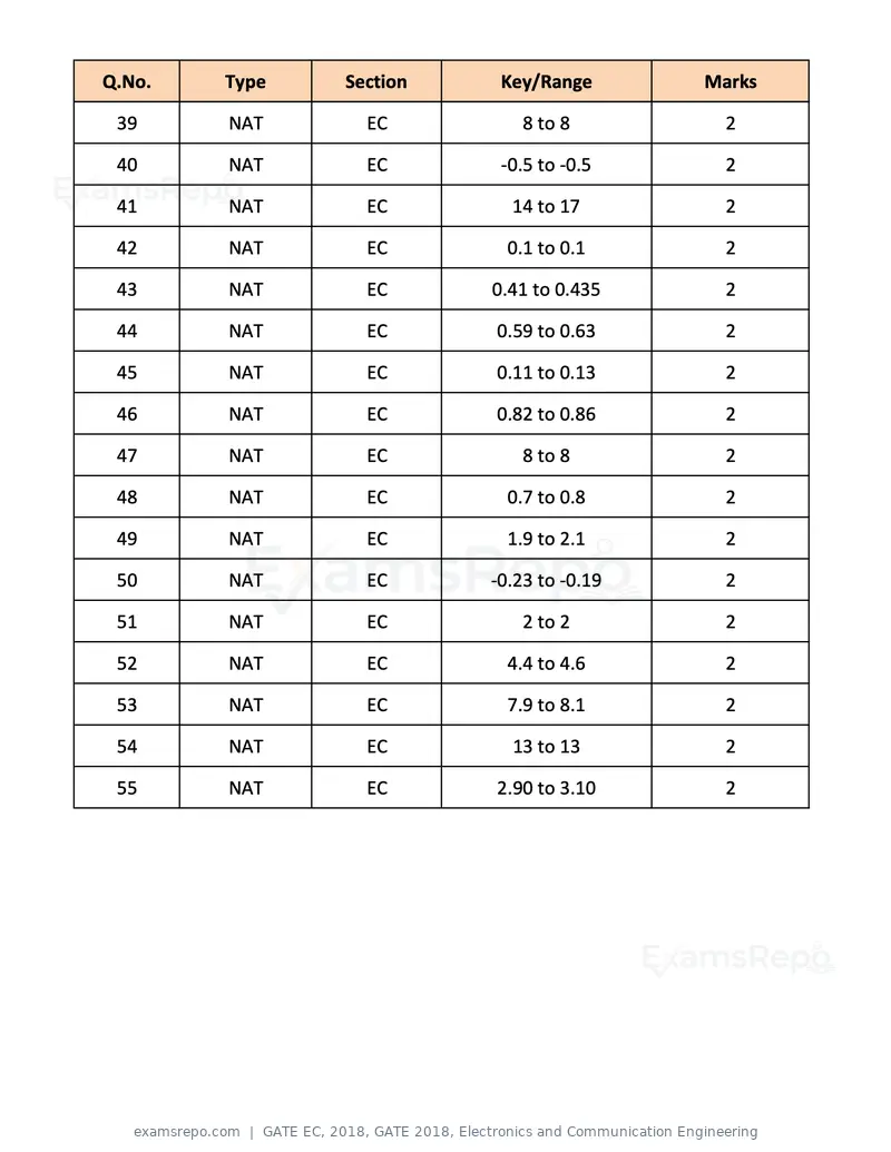
Q.No.   Type   Section    Key/Range       Marks

 15     NAT      EC       0.12 to 0.13     1

 16     NAT      EC         16 to 16       1

 17     NAT      EC       0.12 to 0.14     1

 18     NAT      EC       0.40 to 0.43     1

 19     NAT      EC          5 to 5        1

 20     NAT      EC       0.47 to 0.51     1

 21     NAT      EC      0.001 to 0.001    1

 22     NAT      EC          2 to 2        1

 23     NAT      EC       0.25 to 0.25     1

 24     NAT      EC      ‐0.01 to 0.01     1

 25     NAT      EC        4.3 to 5.3      1

 26     MCQ      EC            B           2

 27     MCQ      EC            D           2

 28     MCQ      EC            B           2

 29     MCQ      EC            A           2

 30     MCQ      EC            B           2

 31     MCQ      EC            C           2

 32     MCQ      EC            A            2

 33     MCQ      EC            B            2

 34     MCQ      EC            A            2

 35     MCQ      EC            C            2

 36     NAT      EC      0.284 to 0.348     2

 37     NAT      EC        6.2 to 6.6       2

 38     NAT      EC        0.4 to 0.6       2
Text of page 23
Q.No.   Type   Section    Key/Range       Marks

 39     NAT      EC          8 to 8        2

 40     NAT      EC       ‐0.5 to ‐0.5      2

 41     NAT      EC        14 to 17         2

 42     NAT      EC        0.1 to 0.1       2

 43     NAT      EC      0.41 to 0.435      2

 44     NAT      EC      0.59 to 0.63       2

 45     NAT      EC      0.11 to 0.13       2

 46     NAT      EC      0.82 to 0.86      2

 47     NAT      EC          8 to 8        2

 48     NAT      EC        0.7 to 0.8      2

 49     NAT      EC        1.9 to 2.1       2

 50     NAT      EC      ‐0.23 to ‐0.19     2

 51     NAT      EC          2 to 2         2

 52     NAT      EC        4.4 to 4.6       2

 53     NAT      EC        7.9 to 8.1       2

 54     NAT      EC        13 to 13         2

 55     NAT      EC      2.90 to 3.10       2
Official key not published for this paper.
Page 1 of 23
Source: GATE. Question paper published by GATE.