
GATE EC 2023: Electronics and Communication Engineering
Text of page 1
Electronics and Communication Engineering (EC)


General Aptitude (GA)
Q.1 – Q.5 Carry ONE mark Each

 Q.1       “I cannot support this proposal. My ________ will not permit it.”


 (A)       conscious


 (B)       consensus


 (C)       conscience


 (D)       consent


 Q.2       Courts : _______ : : Parliament : Legislature

           (By word meaning)


 (A)       Judiciary


 (B)       Executive


 (C)       Governmental


 (D)       Legal


                                          Page 1 of 44
Organizing Institute: IIT Kanpur
Text of page 2
Electronics and Communication Engineering (EC)


 Q.3       What is the smallest number with distinct digits whose digits add up to 45?


 (A)       123555789


 (B)       123457869


 (C)       123456789


 (D)       99999


 Q.4       In a class of 100 students,

            (i)    there are 30 students who neither like romantic movies nor comedy movies,
           (ii)    the number of students who like romantic movies is twice the number of
                   students who like comedy movies, and
           (iii)   the number of students who like both romantic movies and comedy movies
                   is 20.

           How many students in the class like romantic movies?


 (A)       40


 (B)       20


 (C)       60


 (D)       30


                                            Page 2 of 44
Organizing Institute: IIT Kanpur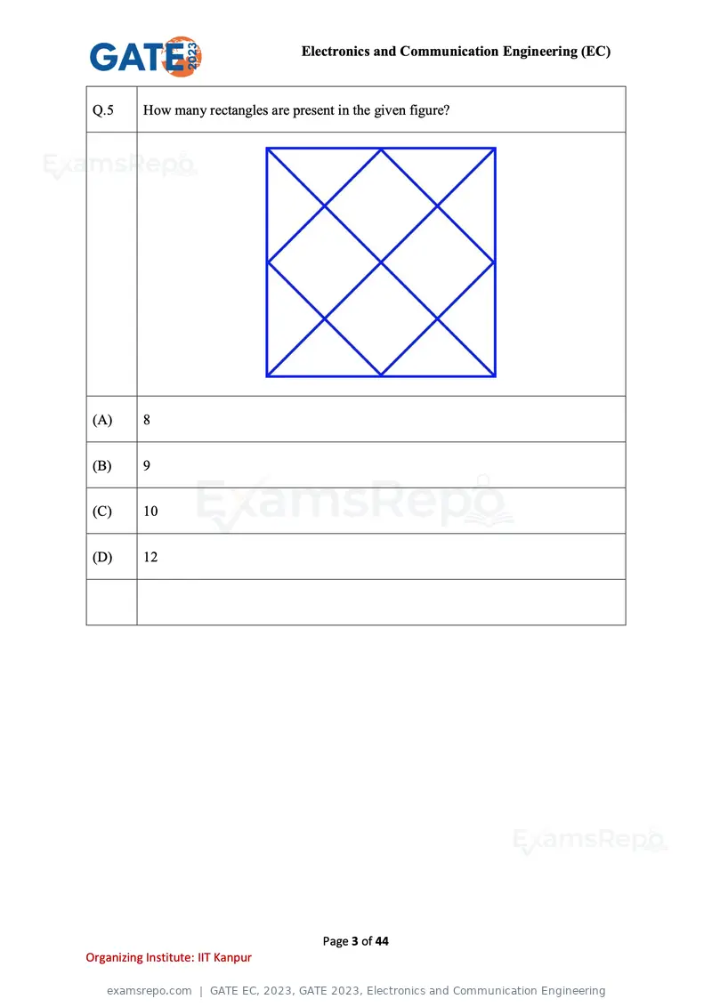
Text of page 3
Electronics and Communication Engineering (EC)


 Q.5       How many rectangles are present in the given figure?


                                   .                                .


 (A)       8


 (B)       9


 (C)       10


 (D)       12


                                          Page 3 of 44
Organizing Institute: IIT Kanpur
Text of page 4
Electronics and Communication Engineering (EC)


Q.6 – Q.10 Carry TWO marks Each

 Q.6       Forestland is a planet inhabited by different kinds of creatures. Among other
           creatures, it is populated by animals all of whom are ferocious. There are also
           creatures that have claws, and some that do not. All creatures that have claws are
           ferocious.

           Based only on the information provided above, which one of the following options
           can be logically inferred with certainty?


 (A)       All creatures with claws are animals.


 (B)       Some creatures with claws are non-ferocious.


 (C)       Some non-ferocious creatures have claws.


 (D)       Some ferocious creatures are creatures with claws.


                                          Page 4 of 44
Organizing Institute: IIT Kanpur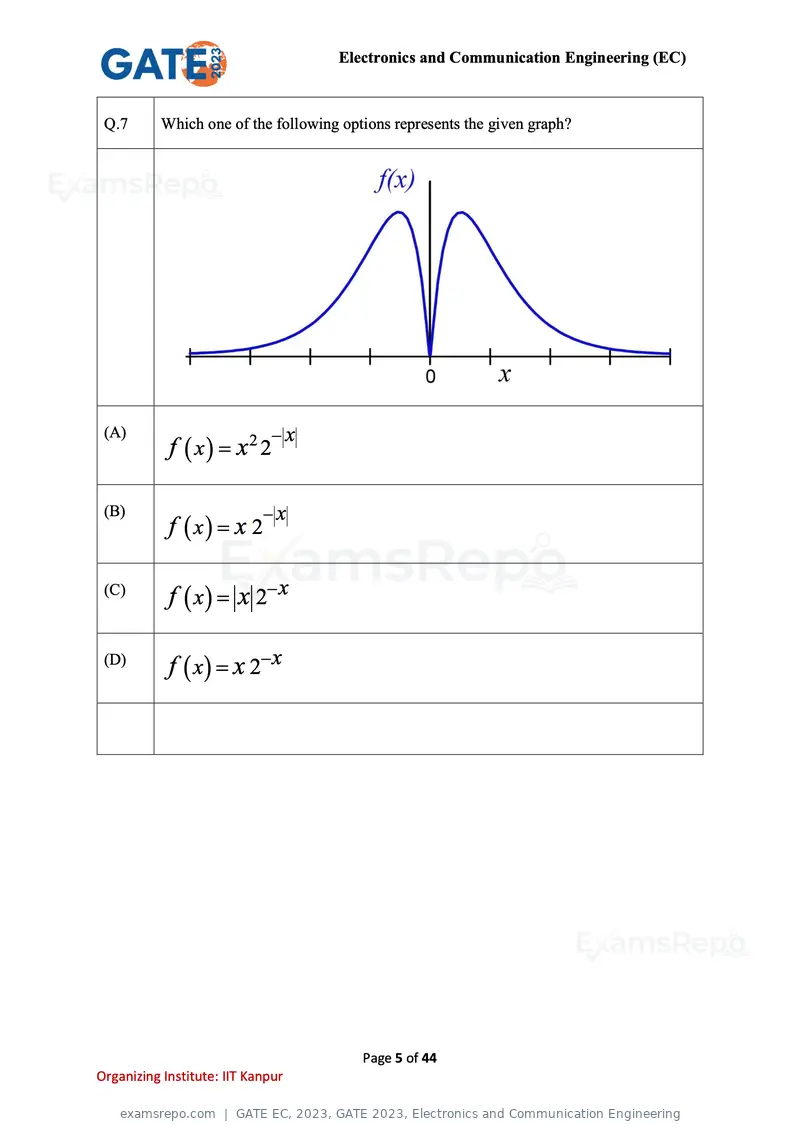
Text of page 5
Electronics and Communication Engineering (EC)


 Q.7       Which one of the following options represents the given graph?


 (A)                          −x
            f ( x ) = x2 2

 (B)                         −x
            f ( x ) = x. 2

 (C)
            f ( x ) = x 2− x

 (D)
            f ( x ) = x. 2− x


                                         Page 5 of 44
Organizing Institute: IIT Kanpur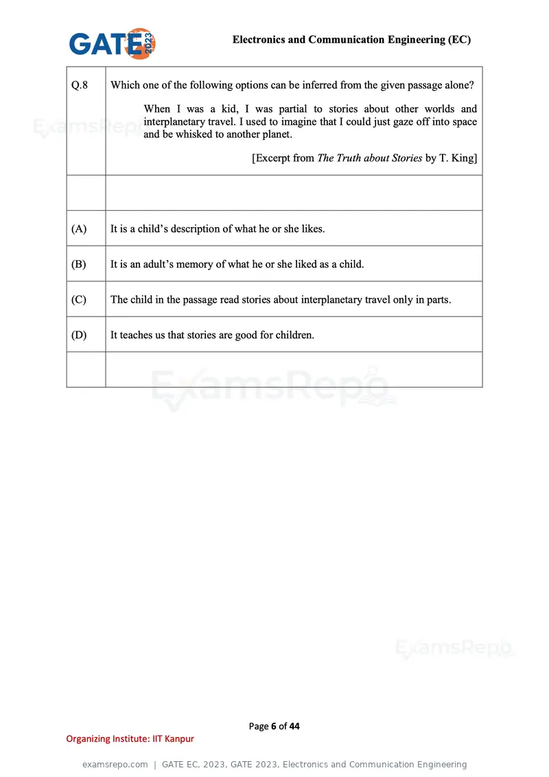
Text of page 6
Electronics and Communication Engineering (EC)


 Q.8       Which one of the following options can be inferred from the given passage alone?

                   When I was a kid, I was partial to stories about other worlds and
                   interplanetary travel. I used to imagine that I could just gaze off into space
                   and be whisked to another planet.

                                             [Excerpt from The Truth about Stories by T. King]


 (A)       It is a child’s description of what he or she likes.


 (B)       It is an adult’s memory of what he or she liked as a child.


 (C)       The child in the passage read stories about interplanetary travel only in parts.


 (D)       It teaches us that stories are good for children.


                                            Page 6 of 44
Organizing Institute: IIT Kanpur
Text of page 7
Electronics and Communication Engineering (EC)


 Q.9       Out of 1000 individuals in a town, 100 unidentified individuals are covid positive.
           Due to lack of adequate covid-testing kits, the health authorities of the town devised
           a strategy to identify these covid-positive individuals. The strategy is to:

                 (i)     Collect saliva samples from all 1000 individuals and randomly group
                         them into sets of 5.

                 (ii)    Mix the samples within each set and test the mixed sample for covid.

                 (iii)   If the test done in (ii) gives a negative result, then declare all the 5
                         individuals to be covid negative.

                 (iv)    If the test done in (ii) gives a positive result, then all the 5 individuals
                         are separately tested for covid.

           Given this strategy, no more than _______ testing kits will be required to identify
           all the 100 covid positive individuals irrespective of how they are grouped.


 (A)       700


 (B)       600


 (C)       800


 (D)       1000


                                              Page 7 of 44
Organizing Institute: IIT Kanpur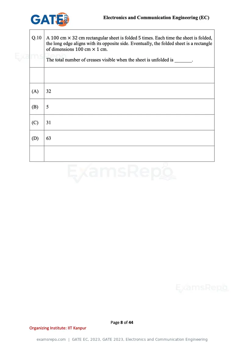
Text of page 8
Electronics and Communication Engineering (EC)


 Q.10 A 100 cm × 32 cm rectangular sheet is folded 5 times. Each time the sheet is folded,
      the long edge aligns with its opposite side. Eventually, the folded sheet is a rectangle
      of dimensions 100 cm × 1 cm.

         The total number of creases visible when the sheet is unfolded is _______.


 (A)     32


 (B)     5


 (C)     31


 (D)     63


                                         Page 8 of 44
Organizing Institute: IIT Kanpur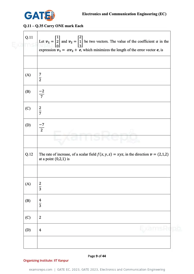
Text of page 9
Electronics and Communication Engineering (EC)


Q.11 – Q.35 Carry ONE mark Each

 Q.11                 1           2
           Let v1 = [2] and v2 = [1] be two vectors. The value of the coefficient α in the
                      0           3
           expression v1 = αv2 + e, which minimizes the length of the error vector e, is


 (A)       7
           2

 (B)       −2
           7

 (C)       2
           7

 (D)       −7
           2


 Q.12      The rate of increase, of a scalar field f(x, y, z) = xyz, in the direction v = (2,1,2)
           at a point (0,2,1) is


 (A)       2
           3

 (B)       4
           3

 (C)       2


 (D)       4


                                           Page 9 of 44
Organizing Institute: IIT Kanpur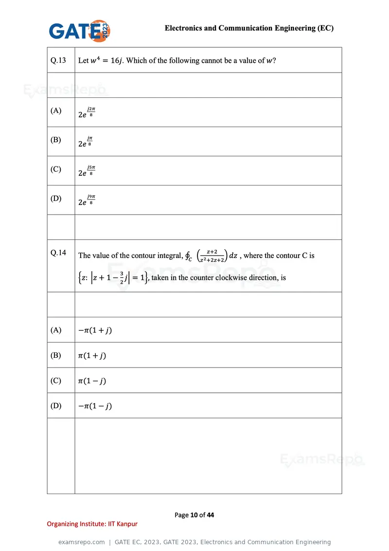
Text of page 10
Electronics and Communication Engineering (EC)


 Q.13      Let w 4 = 16j. Which of the following cannot be a value of w?


              j2π
 (A)
           2e 8

              jπ
 (B)
           2e 8

              j5π
 (C)
           2e 8

              j9π
 (D)
           2e 8


 Q.14                                                z+2
           The value of the contour integral, ∮C (z 2 +2z+2) dz , where the contour C is

                         3
           {z: |z + 1 − 2 j| = 1}, taken in the counter clockwise direction, is


 (A)       −π(1 + j)


 (B)       π(1 + j)


 (C)       π(1 − j)


 (D)       −π(1 − j)


                                          Page 10 of 44
Organizing Institute: IIT Kanpur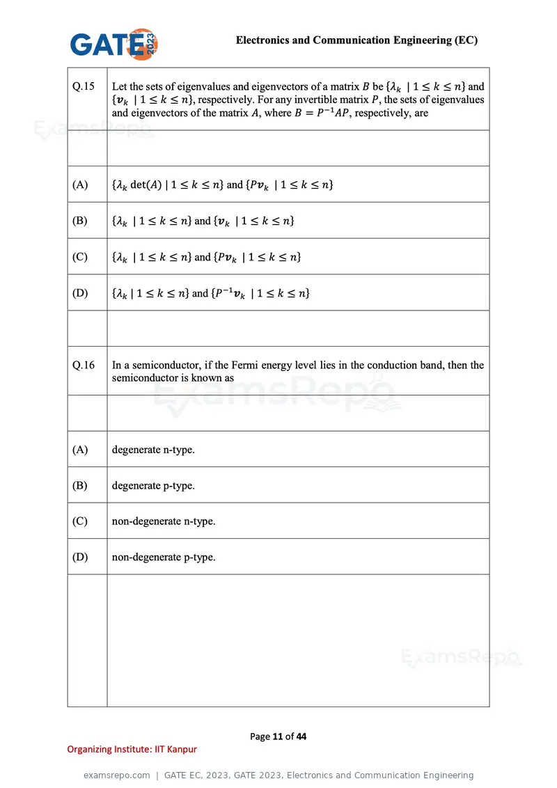
Text of page 11
Electronics and Communication Engineering (EC)


 Q.15      Let the sets of eigenvalues and eigenvectors of a matrix B be {λk | 1 ≤ k ≤ n} and
           {vk | 1 ≤ k ≤ n}, respectively. For any invertible matrix P, the sets of eigenvalues
           and eigenvectors of the matrix A, where B = P −1 AP, respectively, are


 (A)       {λk det(A) | 1 ≤ k ≤ n} and {Pvk | 1 ≤ k ≤ n}


 (B)       {λk | 1 ≤ k ≤ n} and {vk | 1 ≤ k ≤ n}


 (C)       {λk | 1 ≤ k ≤ n} and {Pvk | 1 ≤ k ≤ n}


 (D)       {λk | 1 ≤ k ≤ n} and {P−1 vk | 1 ≤ k ≤ n}


 Q.16      In a semiconductor, if the Fermi energy level lies in the conduction band, then the
           semiconductor is known as


 (A)       degenerate n-type.


 (B)       degenerate p-type.


 (C)       non-degenerate n-type.


 (D)       non-degenerate p-type.


                                          Page 11 of 44
Organizing Institute: IIT Kanpur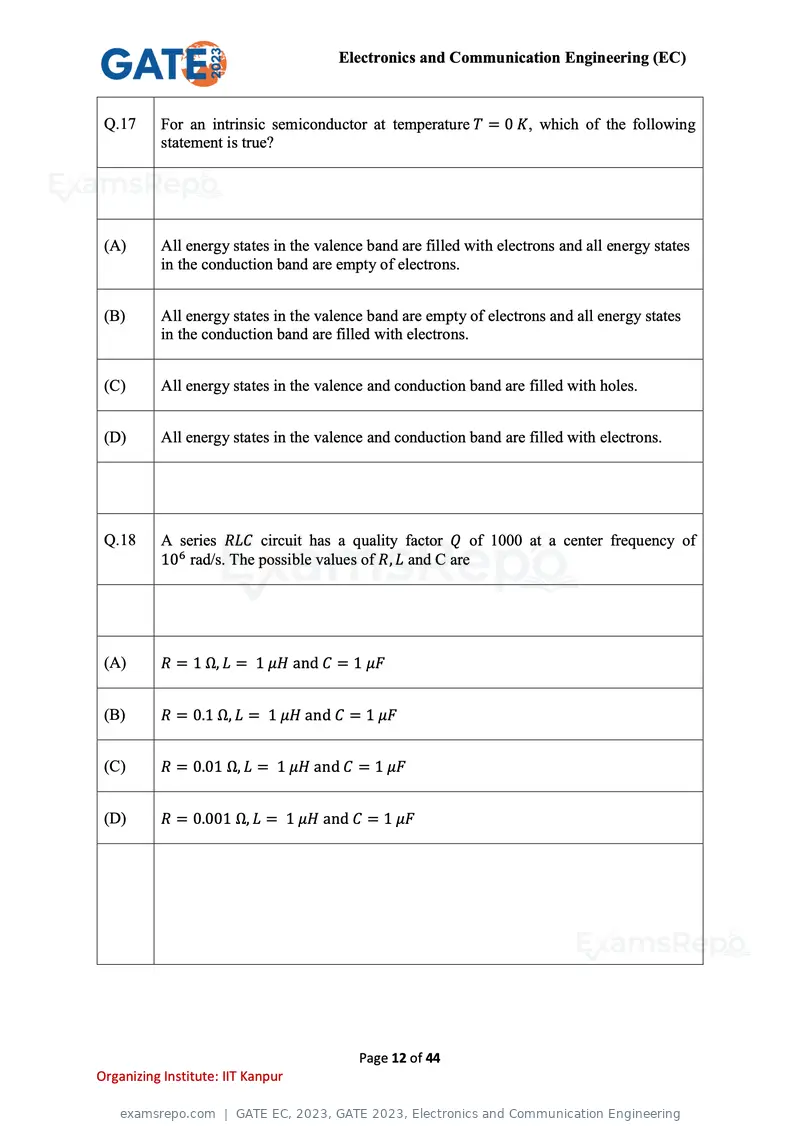
Text of page 12
Electronics and Communication Engineering (EC)


 Q.17      For an intrinsic semiconductor at temperature T = 0 K, which of the following
           statement is true?


 (A)       All energy states in the valence band are filled with electrons and all energy states
           in the conduction band are empty of electrons.


 (B)       All energy states in the valence band are empty of electrons and all energy states
           in the conduction band are filled with electrons.


 (C)       All energy states in the valence and conduction band are filled with holes.


 (D)       All energy states in the valence and conduction band are filled with electrons.


 Q.18      A series RLC circuit has a quality factor Q of 1000 at a center frequency of
           106 rad/s. The possible values of R, L and C are


 (A)       R = 1 Ω, L = 1 μH and C = 1 μF


 (B)       R = 0.1 Ω, L = 1 μH and C = 1 μF


 (C)       R = 0.01 Ω, L = 1 μH and C = 1 μF


 (D)       R = 0.001 Ω, L = 1 μH and C = 1 μF


                                          Page 12 of 44
Organizing Institute: IIT Kanpur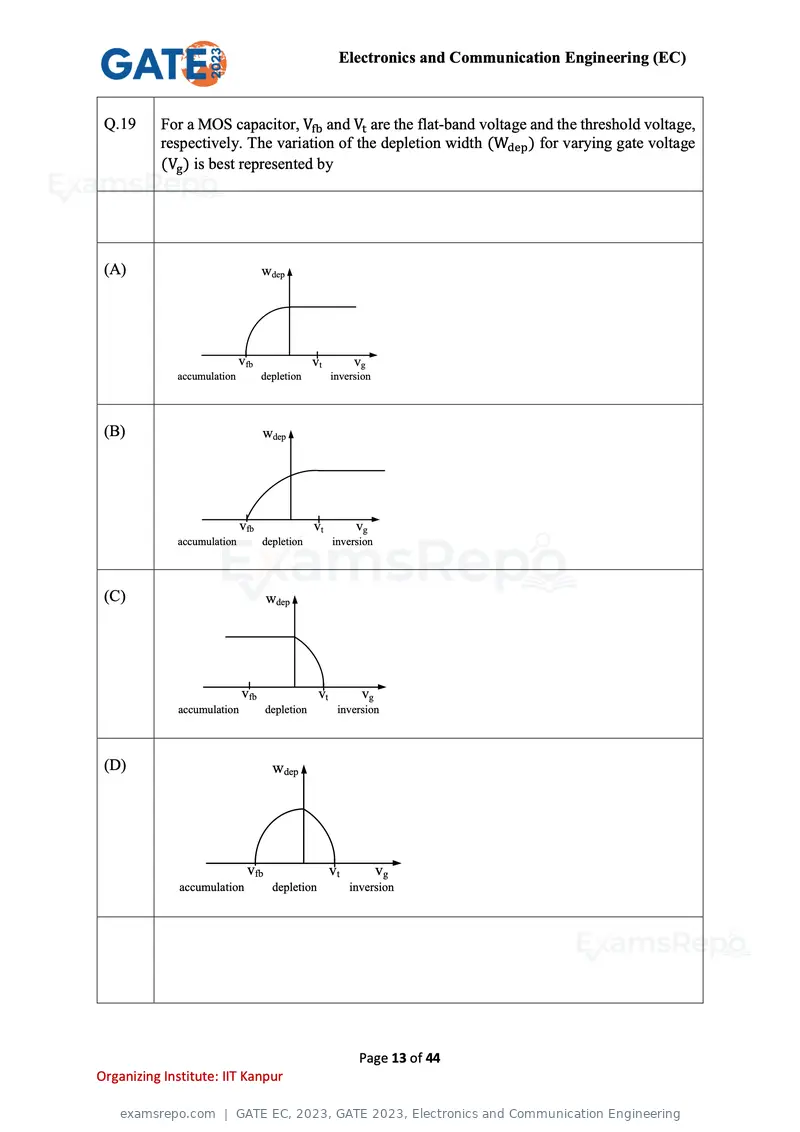
Text of page 13
Electronics and Communication Engineering (EC)


 Q.19      For a MOS capacitor, Vfb and Vt are the flat-band voltage and the threshold voltage,
           respectively. The variation of the depletion width (Wdep ) for varying gate voltage
           (Vg ) is best represented by


 (A)                              wdep


                            vfb                vt         vg
             accumulation         depletion          inversion


 (B)                              wdep


                            vfb                vt          vg
             accumulation         depletion          inversion


 (C)                               wdep


                            vfb                 vt          vg
             accumulation          depletion          inversion


 (D)                                wdep


                             vfb                     vt          vg
              accumulation          depletion             inversion


                                                            Page 13 of 44
Organizing Institute: IIT Kanpur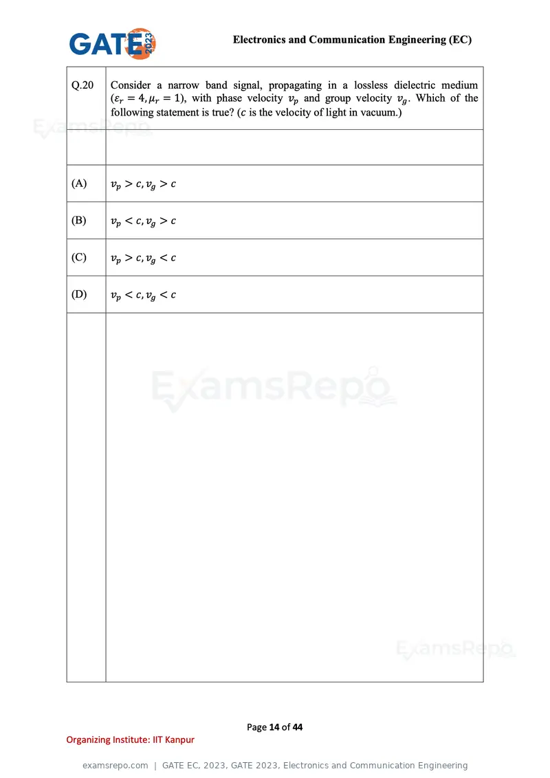
Text of page 14
Electronics and Communication Engineering (EC)


 Q.20      Consider a narrow band signal, propagating in a lossless dielectric medium
           (εr = 4, μr = 1), with phase velocity vp and group velocity vg . Which of the
           following statement is true? (c is the velocity of light in vacuum.)


 (A)       vp > c, vg > c


 (B)       vp < c, vg > c


 (C)       vp > c, vg < c


 (D)       vp < c, vg < c


                                       Page 14 of 44
Organizing Institute: IIT Kanpur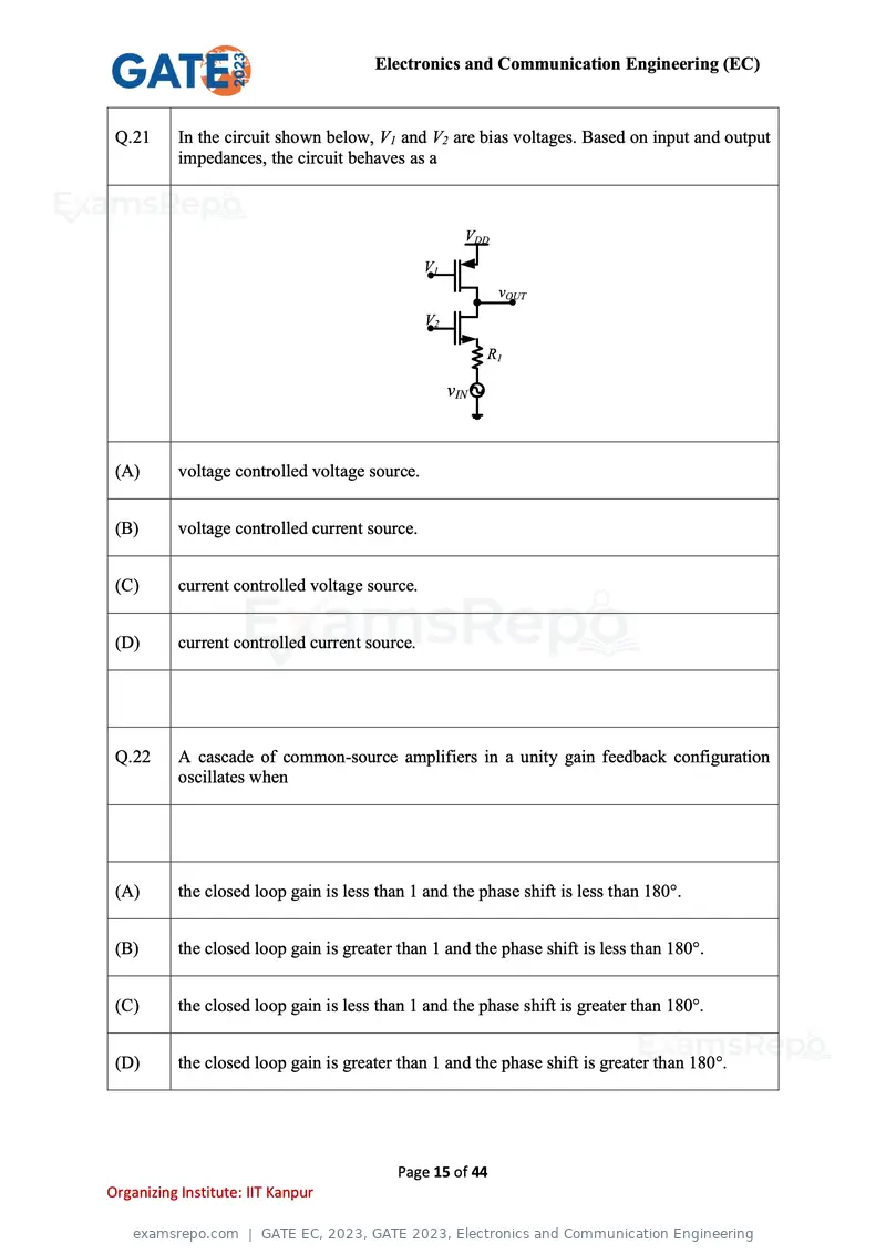
Text of page 15
Electronics and Communication Engineering (EC)


 Q.21      In the circuit shown below, V1 and V2 are bias voltages. Based on input and output
           impedances, the circuit behaves as a


                                                       VDD
                                                V1
                                                             vOUT
                                                V2

                                                           R1

                                                     vIN


 (A)       voltage controlled voltage source.


 (B)       voltage controlled current source.


 (C)       current controlled voltage source.


 (D)       current controlled current source.


 Q.22      A cascade of common-source amplifiers in a unity gain feedback configuration
           oscillates when


 (A)       the closed loop gain is less than 1 and the phase shift is less than 180°.


 (B)       the closed loop gain is greater than 1 and the phase shift is less than 180°.


 (C)       the closed loop gain is less than 1 and the phase shift is greater than 180°.


 (D)       the closed loop gain is greater than 1 and the phase shift is greater than 180°.


                                           Page 15 of 44
Organizing Institute: IIT Kanpur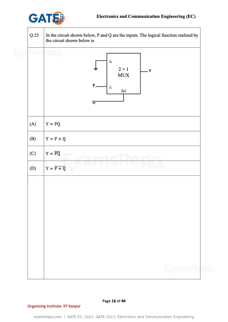
Text of page 16
Electronics and Communication Engineering (EC)


 Q.23      In the circuit shown below, P and Q are the inputs. The logical function realized by
           the circuit shown below is


                                             I0

                                                  2×1              Y
                                                  MUX

                                    P        I1
                                                    Sel

                                    Q


 (A)       Y = PQ


 (B)       Y=P+Q


 (C)       Y = ̅̅̅̅
               PQ


 (D)       Y = ̅̅̅̅̅̅̅
               P+Q


                                          Page 16 of 44
Organizing Institute: IIT Kanpur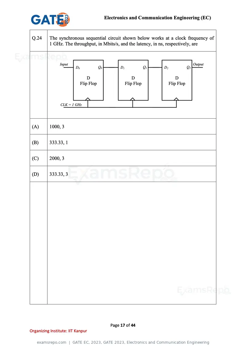
Text of page 17
Electronics and Communication Engineering (EC)


 Q.24      The synchronous sequential circuit shown below works at a clock frequency of
           1 GHz. The throughput, in Mbits/s, and the latency, in ns, respectively, are


                Input                                                                             Output
                         D0               Q0          D1               Q1   D2               Q2

                                  D                            D                     D
                              Flip Flop                    Flip Flop             Flip Flop


                 CLK = 1 GHz


 (A)       1000, 3


 (B)       333.33, 1


 (C)       2000, 3


 (D)       333.33, 3


                                                 Page 17 of 44
Organizing Institute: IIT Kanpur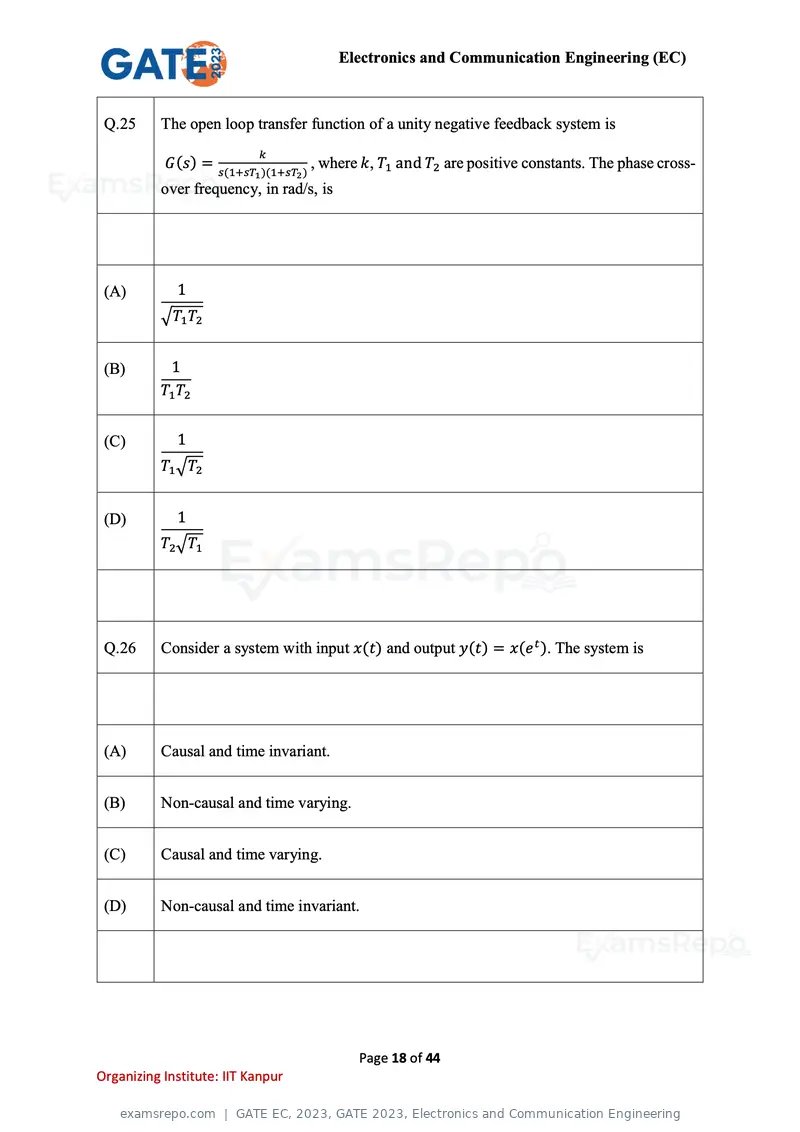
Text of page 18
Electronics and Communication Engineering (EC)


 Q.25      The open loop transfer function of a unity negative feedback system is
                           k
           G(s) = s(1+sT )(1+sT ) , where k, T1 and T2 are positive constants. The phase cross-
                           1       2
           over frequency, in rad/s, is


 (A)         1
           √T1 T2


 (B)        1
           T1 T2


 (C)         1
           T1 √T2


 (D)         1
           T2 √T1


 Q.26      Consider a system with input x(t) and output y(t) = x(e t ). The system is


 (A)       Causal and time invariant.


 (B)       Non-causal and time varying.


 (C)       Causal and time varying.


 (D)       Non-causal and time invariant.


                                            Page 18 of 44
Organizing Institute: IIT Kanpur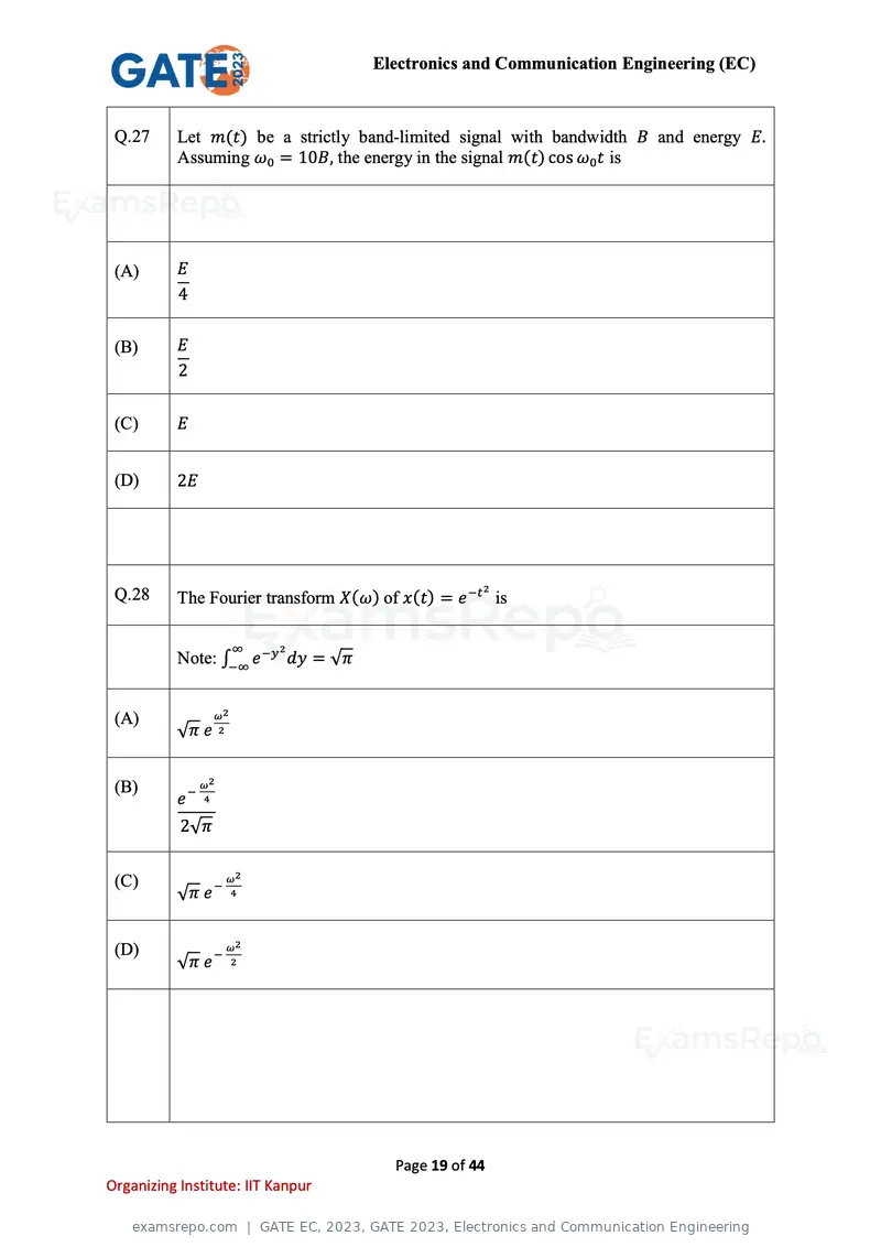
Text of page 19
Electronics and Communication Engineering (EC)


 Q.27      Let m(t) be a strictly band-limited signal with bandwidth B and energy E.
           Assuming ω0 = 10B, the energy in the signal m(t) cos ω0 t is


 (A)       E
           4

 (B)       E
           2

 (C)       E


 (D)       2E


                                                    2
 Q.28      The Fourier transform X(ω) of x(t) = e −t is

                       ∞   2
           Note: ∫−∞ e −y dy = √π


 (A)              ω2
           √π e    2


 (B)            ω2
           e− 4
           2√π


 (C)                  ω2
                  −
           √π e        4


 (D)                  ω2
                  −
           √π e        2


                                        Page 19 of 44
Organizing Institute: IIT Kanpur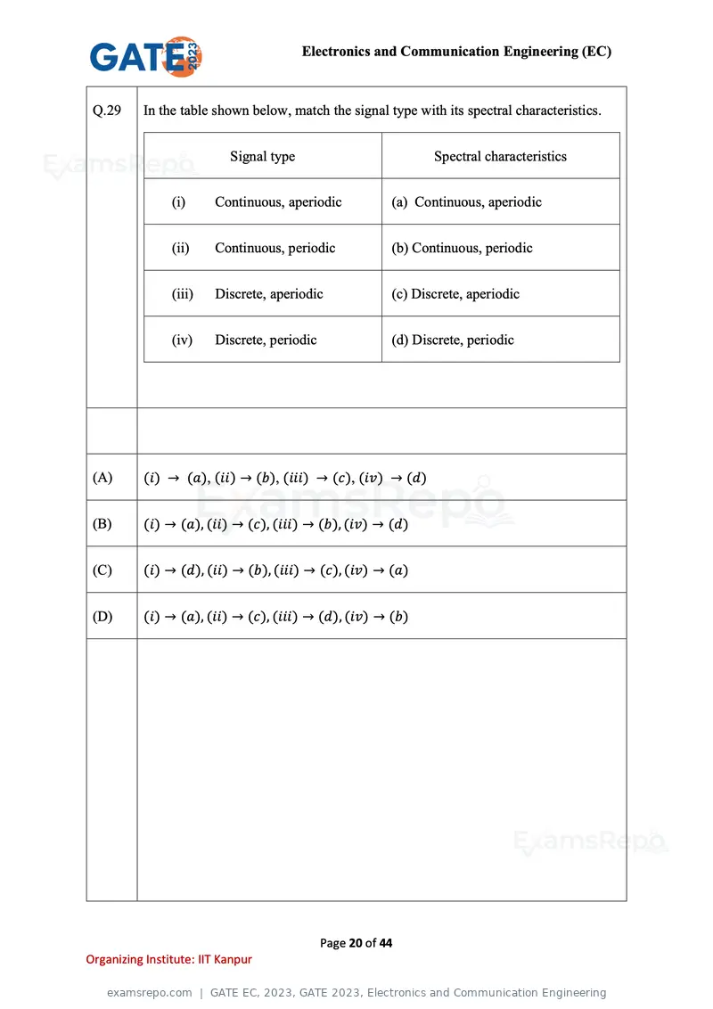
Text of page 20
Electronics and Communication Engineering (EC)


 Q.29      In the table shown below, match the signal type with its spectral characteristics.


                           Signal type                          Spectral characteristics


                (i)     Continuous, aperiodic            (a) Continuous, aperiodic


                (ii)    Continuous, periodic             (b) Continuous, periodic


                (iii)   Discrete, aperiodic              (c) Discrete, aperiodic


                (iv)    Discrete, periodic               (d) Discrete, periodic


           .


 (A)       (i) → (a), (ii) → (b), (iii) → (c), (iv) → (d)


 (B)       (i) → (a), (ii) → (c), (iii) → (b), (iv) → (d)


 (C)       (i) → (d), (ii) → (b), (iii) → (c), (iv) → (a)


 (D)       (i) → (a), (ii) → (c), (iii) → (d), (iv) → (b)


                                             Page 20 of 44
Organizing Institute: IIT Kanpur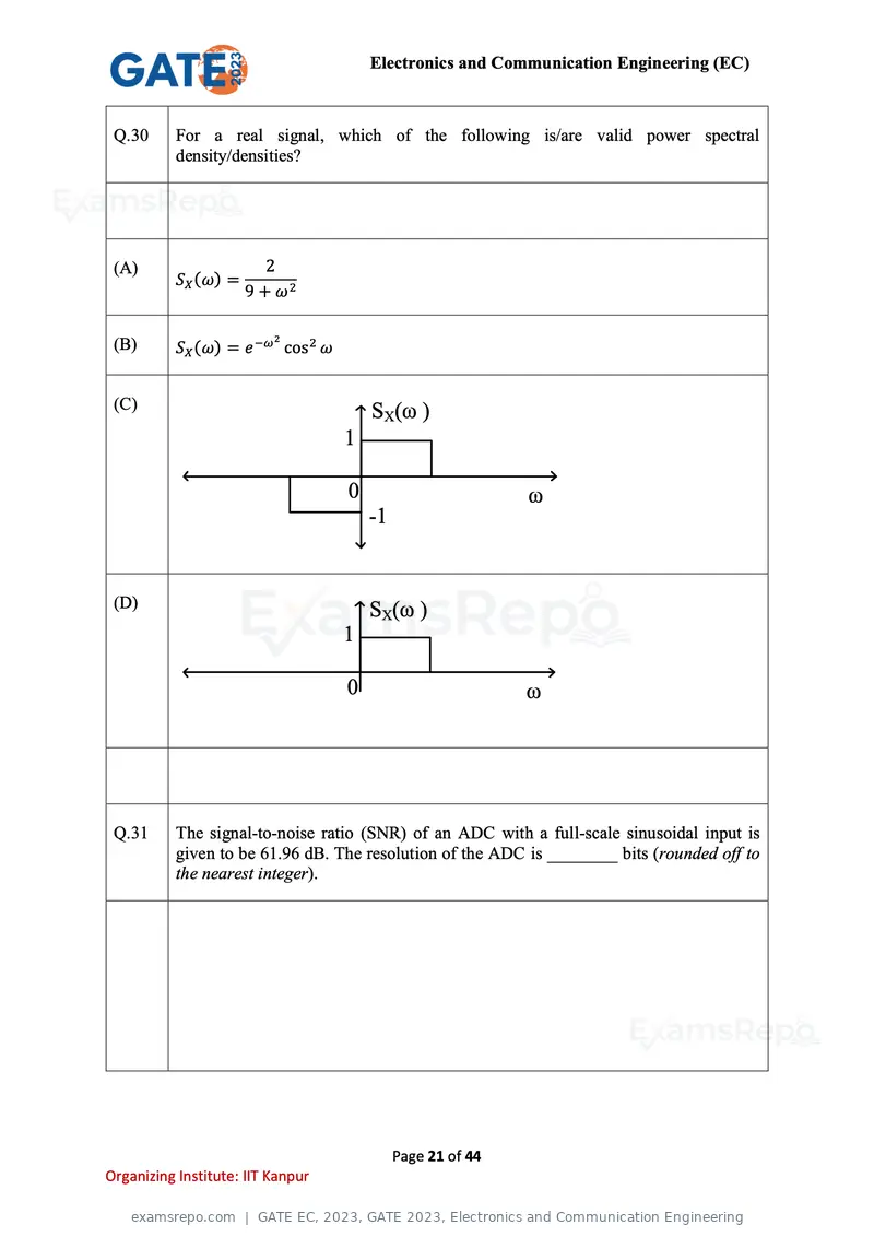
Text of page 21
Electronics and Communication Engineering (EC)


 Q.30      For a real signal, which of the following is/are valid power spectral
           density/densities?


 (A)                     2
           SX (ω) =
                      9 + ω2

                          2
 (B)       SX (ω) = e −ω cos2 ω


 (C)                                   SX(ω )
                                   1

                                   0                        ω
                                       -1


 (D)                                   SX(ω )
                                   1

                                   0                        ω


 Q.31      The signal-to-noise ratio (SNR) of an ADC with a full-scale sinusoidal input is
           given to be 61.96 dB. The resolution of the ADC is ________ bits (rounded off to
           the nearest integer).


                                            Page 21 of 44
Organizing Institute: IIT Kanpur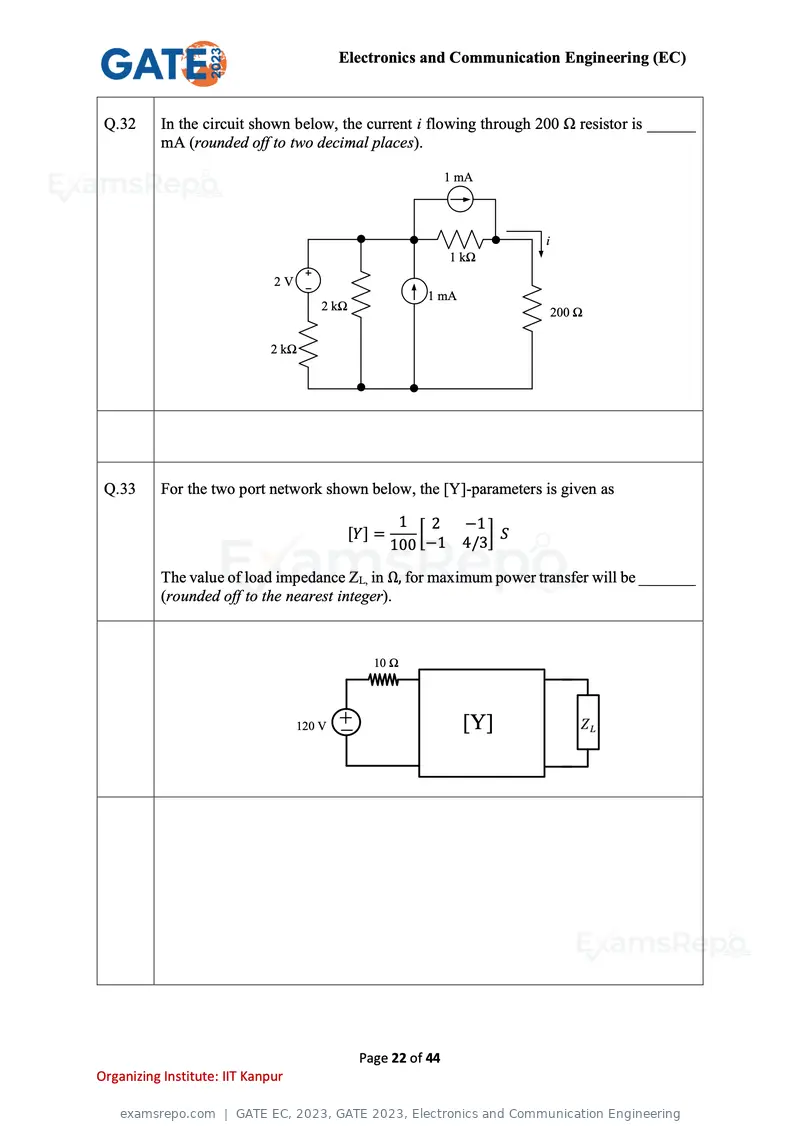
Text of page 22
Electronics and Communication Engineering (EC)


 Q.32      In the circuit shown below, the current i flowing through 200 Ω resistor is ______
           mA (rounded off to two decimal places).

                                                                1 mA


                                                                        i
                                                                1 kΩ
                              2V
                                                          1 mA
                                       2 kΩ                                 200 Ω

                             2 kΩ


 Q.33      For the two port network shown below, the [Y]-parameters is given as

                                                     1 2     −1
                                            [Y] =       [       ]S
                                                    100   −1 4/3

           The value of load impedance ZL, in Ω, for maximum power transfer will be _______
           (rounded off to the nearest integer).


                                                  10 Ω


                                   120 V   +_                     [Y]


                                                Page 22 of 44
Organizing Institute: IIT Kanpur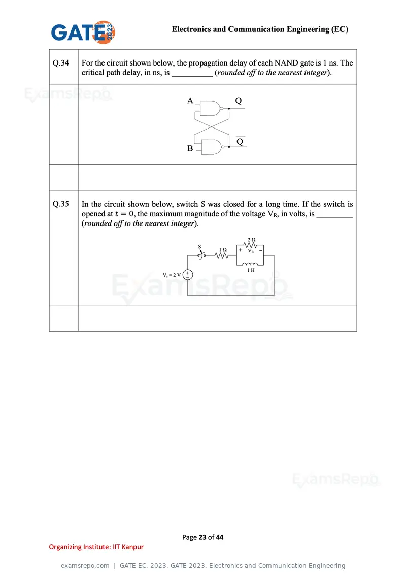
Text of page 23
Electronics and Communication Engineering (EC)


 Q.34      For the circuit shown below, the propagation delay of each NAND gate is 1 ns. The
           critical path delay, in ns, is __________ (rounded off to the nearest integer).


                                               A              Q


                                                              Q
                                               B


 Q.35      In the circuit shown below, switch S was closed for a long time. If the switch is
           opened at t = 0, the maximum magnitude of the voltage VR, in volts, is _________
           (rounded off to the nearest integer).
                                                                  2Ω
                                                   S
                                                         1Ω       VR


                                                                  1H
                                   Vs = 2 V


                                              Page 23 of 44
Organizing Institute: IIT Kanpur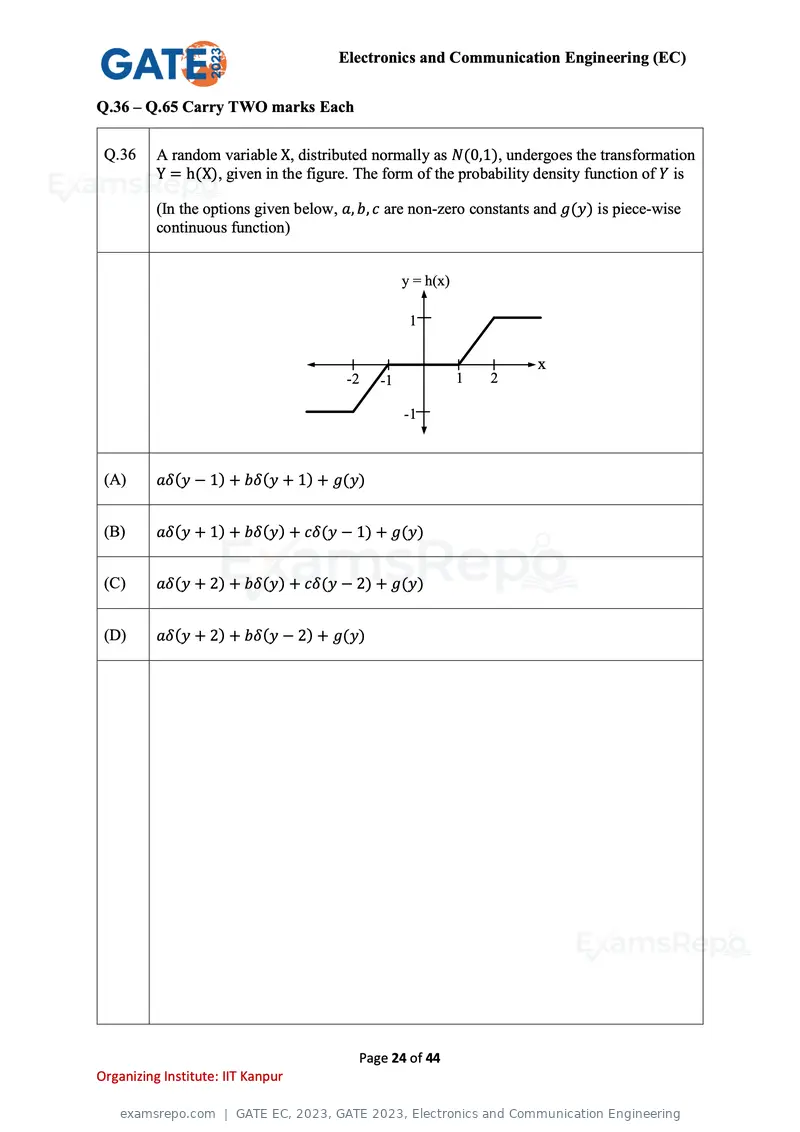
Text of page 24
Electronics and Communication Engineering (EC)


Q.36 – Q.65 Carry TWO marks Each

 Q.36     A random variable X, distributed normally as N(0,1), undergoes the transformation
          Y = h(X), given in the figure. The form of the probability density function of Y is

          (In the options given below, a, b, c are non-zero constants and g(y) is piece-wise
          continuous function)


                                                  y = h(x)

                                                   1

                                                                     x
                                       -2    -1              1   2

                                                  -1


 (A)      aδ(y − 1) + bδ(y + 1) + g(y)


 (B)      aδ(y + 1) + bδ(y) + cδ(y − 1) + g(y)


 (C)      aδ(y + 2) + bδ(y) + cδ(y − 2) + g(y)


 (D)      aδ(y + 2) + bδ(y − 2) + g(y)


                                         Page 24 of 44
Organizing Institute: IIT Kanpur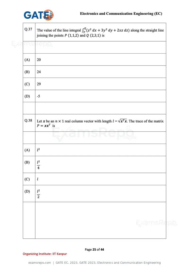
Text of page 25
Electronics and Communication Engineering (EC)


 Q.37                                    Q
          The value of the line integral ∫P (z 2 dx + 3y 2 dy + 2xz dz) along the straight line
          joining the points P (1,1,2) and Q (2,3,1) is


 (A)      20


 (B)      24


 (C)      29


 (D)      -5


 Q.38     Let x be an n × 1 real column vector with length l = √xT x. The trace of the matrix
          P = xxT is


 (A)      l2


 (B)      l2
          4

 (C)      l


 (D)      l2
          2


                                          Page 25 of 44
Organizing Institute: IIT Kanpur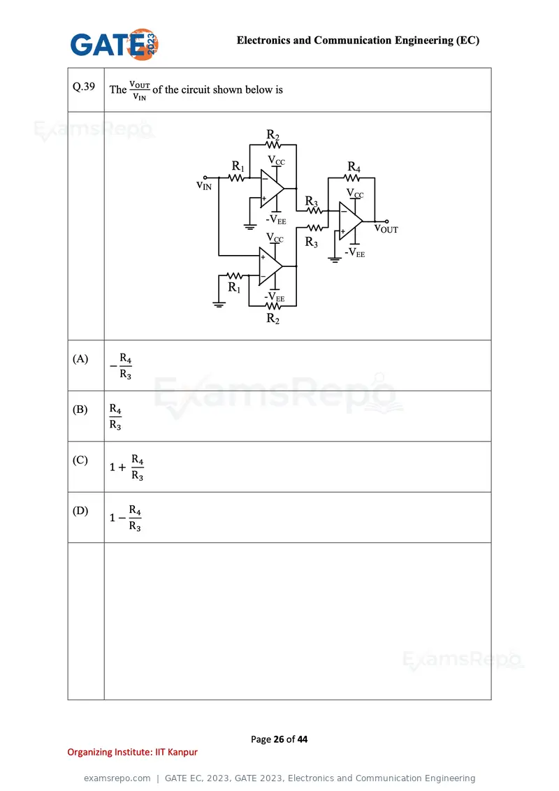
Text of page 26
Electronics and Communication Engineering (EC)


 Q.39          V
          The VOUT of the circuit shown below is
                   IN


                                                R2
                                             VCC
                                     R1                         R4
                                            _
                               vIN
                                            +
                                                             VCC
                                                       R3   _
                                                -VEE
                                                            +        vOUT
                                                VCC    R3
                                            +
                                                            -VEE
                                            _
                                     R1
                                             -VEE

                                                R2


 (A)          R4
          −
              R3


 (B)      R4
          R3


 (C)           R4
          1+
               R3


 (D)           R4
          1−
               R3


                                          Page 26 of 44
Organizing Institute: IIT Kanpur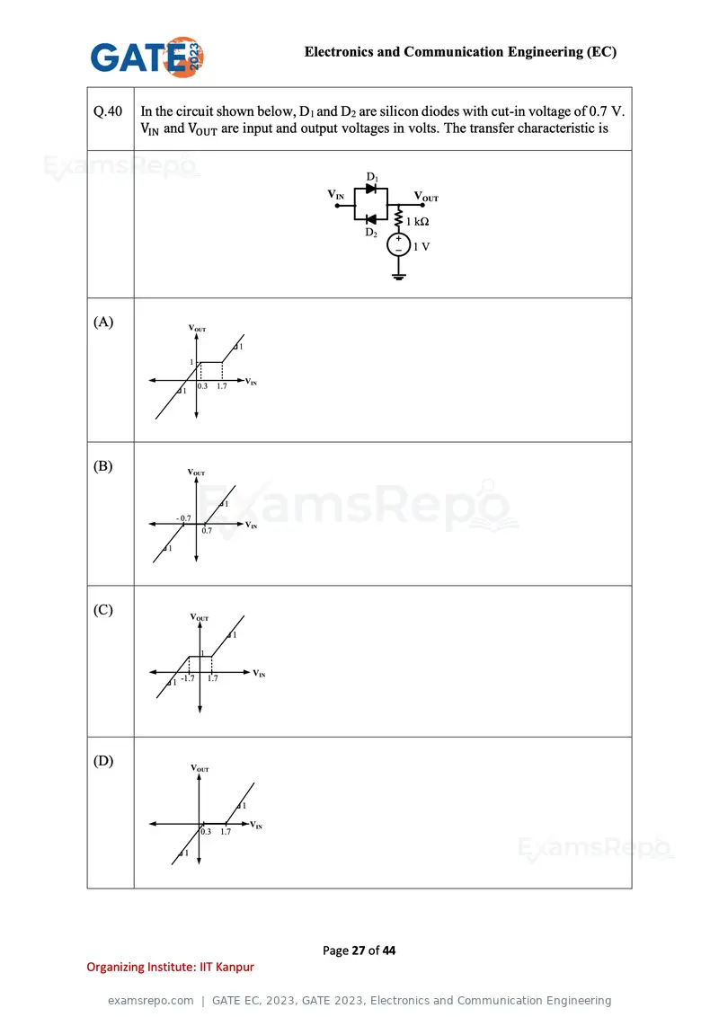
Text of page 27
Electronics and Communication Engineering (EC)


 Q.40     In the circuit shown below, D1 and D2 are silicon diodes with cut-in voltage of 0.7 V.
          VIN and VOUT are input and output voltages in volts. The transfer characteristic is


                                                                       D1
                                                                 VIN             VOUT

                                                                                1 kΩ
                                                                       D2
                                                                            +
                                                                            _    1V


 (A)                     VOUT

                                                  1
                          1

                                                      VIN
                              0.3    1.7
                     1


 (B)                     VOUT


                                         1
                   - 0.7
                                                      VIN
                               0.7

               1


 (C)                      VOUT

                                              1

                              1

                                                        VIN
                   1 -1.7         1.7


 (D)                      VOUT


                                                  1

                                                       VIN
                              0.3       1.7

                      1


                                                                Page 27 of 44
Organizing Institute: IIT Kanpur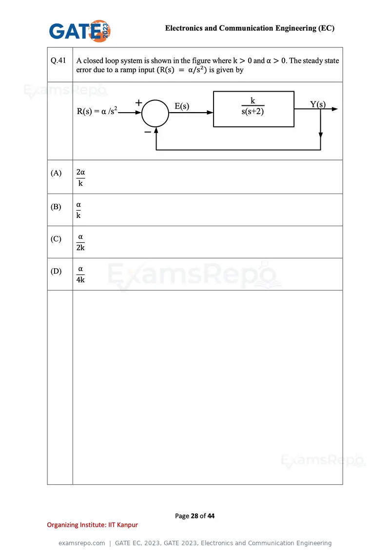
Text of page 28
Electronics and Communication Engineering (EC)


 Q.41     A closed loop system is shown in the figure where k > 0 and α > 0. The steady state
          error due to a ramp input (R(s) = α/s2 ) is given by


                                                                 k                 Y(s)
                        2                E(s)
          R(s) = α /s                                         s(s+2)


 (A)      2α
           k

 (B)      α
          k

 (C)      α
          2k

 (D)      α
          4k


                                         Page 28 of 44
Organizing Institute: IIT Kanpur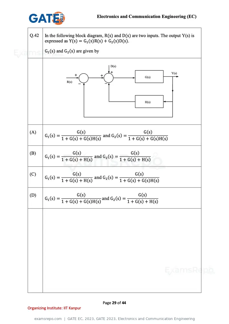
Text of page 29
Electronics and Communication Engineering (EC)


 Q.42     In the following block diagram, R(s) and D(s) are two inputs. The output Y(s) is
          expressed as Y(s) = G1 (s)R(s) + G2 (s)D(s).

          G1 (s) and G2 (s) are given by


                                               D(s)

                                                                             Y(s)
                                                               G(s)
                       R(s)


                                                               H(s)


 (A)                        G(s)                             G(s)
          G1 (s) =                       and G2 (s) =
                     1 + G(s) + G(s)H(s)              1 + G(s) + G(s)H(s)


 (B)                      G(s)                         G(s)
          G1 (s) =                   and G2 (s) =
                     1 + G(s) + H(s)              1 + G(s) + H(s)


 (C)                      G(s)                           G(s)
          G1 (s) =                   and G2 (s) =
                     1 + G(s) + H(s)              1 + G(s) + G(s)H(s)


 (D)                        G(s)                           G(s)
          G1 (s) =                       and G2 (s) =
                     1 + G(s) + G(s)H(s)              1 + G(s) + H(s)


                                           Page 29 of 44
Organizing Institute: IIT Kanpur
Text of page 30
Electronics and Communication Engineering (EC)


 Q.43     The state equation of a second order system is

          ẋ (t) = Ax(t),     x(0) is the initial condition.

          Suppose λ1 and λ2 are two distinct eigenvalues of A and v1 and v2 are the
          corresponding eigenvectors. For constants α1 and α2 , the solution, x(t), of the state
          equation is


 (A)       2

          ∑ αi e λi t vi
          i=1


 (B)       2

          ∑ αi e 2λi t vi
          i=1


 (C)       2

          ∑ αi e 3λi t vi
          i=1


 (D)       2

          ∑ αi e 4λi t vi
          i=1


                                           Page 30 of 44
Organizing Institute: IIT Kanpur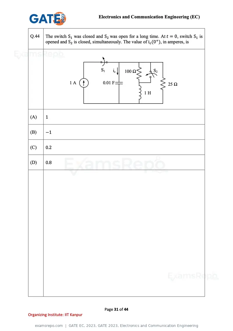
Text of page 31
Electronics and Communication Engineering (EC)


 Q.44     The switch S1 was closed and S2 was open for a long time. At t = 0, switch S1 is
          opened and S2 is closed, simultaneously. The value of ic (0+ ), in amperes, is


                                      S1    ic    100 Ω          S2

                        1A             0.01 F                           25 Ω
                                                            1H


 (A)      1


 (B)      −1


 (C)      0.2


 (D)      0.8


                                        Page 31 of 44
Organizing Institute: IIT Kanpur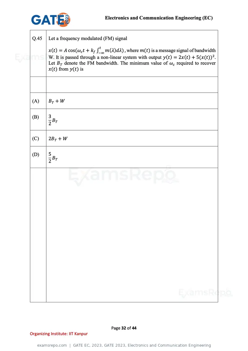
Text of page 32
Electronics and Communication Engineering (EC)


 Q.45     Let a frequency modulated (FM) signal
                                   t
          x(t) = A cos(ωc t + kf ∫−∞ m(λ)dλ) , where m(t) is a message signal of bandwidth
          W. It is passed through a non-linear system with output y(t) = 2x(t) + 5(x(t))2 .
          Let BT denote the FM bandwidth. The minimum value of ωc required to recover
          x(t) from y(t) is


 (A)      BT + W


 (B)      3
            B
          2 T

 (C)      2BT + W


 (D)      5
            B
          2 T


                                         Page 32 of 44
Organizing Institute: IIT Kanpur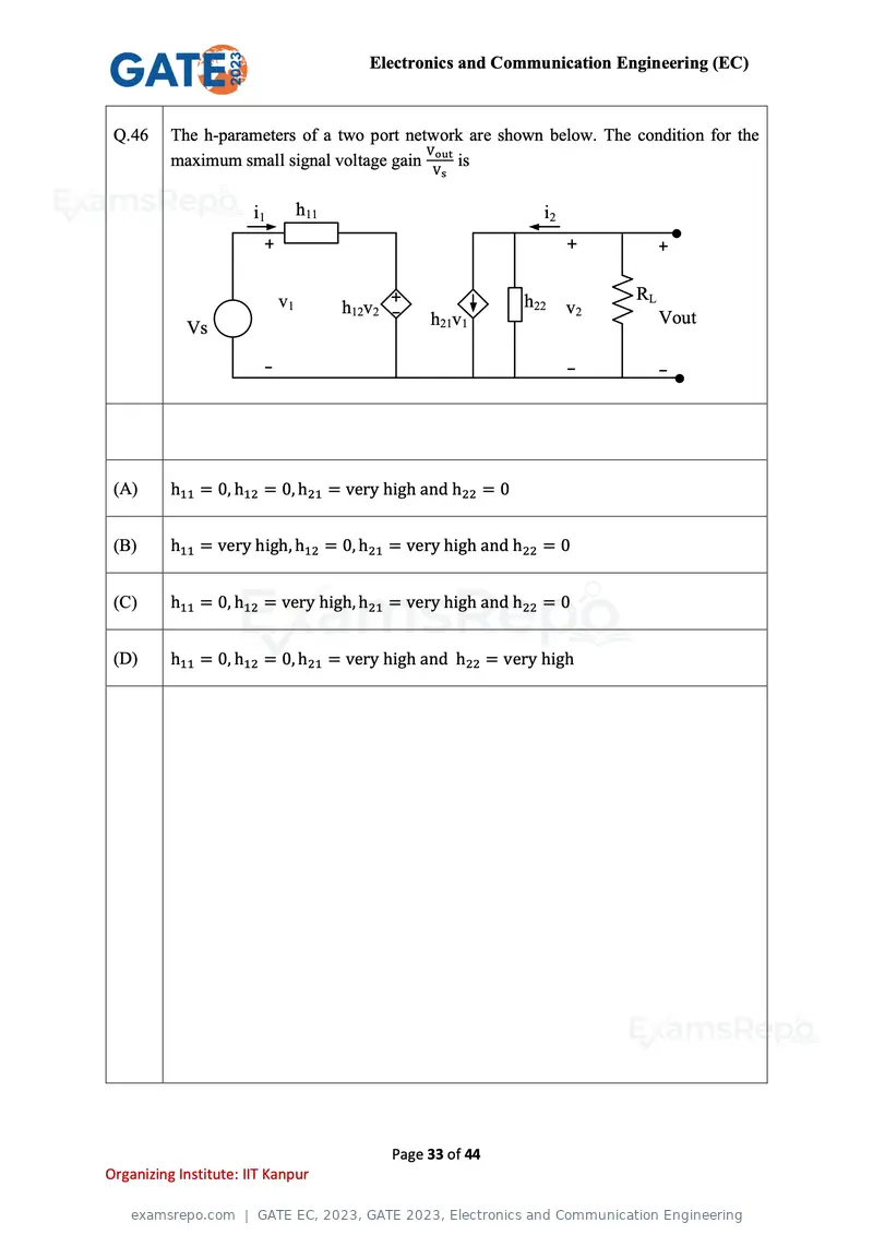
Text of page 33
Electronics and Communication Engineering (EC)


 Q.46     The h-parameters of a two port network are shown below. The condition for the
                                            V
          maximum small signal voltage gain Vout is
                                                      s


                       i1        h11                             i2


                            v1                                 h22         RL
                                       h12v2                          v2
                                                    h21v1                       Vout
            Vs


 (A)      h11 = 0, h12 = 0, h21 = very high and h22 = 0


 (B)      h11 = very high, h12 = 0, h21 = very high and h22 = 0


 (C)      h11 = 0, h12 = very high, h21 = very high and h22 = 0


 (D)      h11 = 0, h12 = 0, h21 = very high and h22 = very high


                                               Page 33 of 44
Organizing Institute: IIT Kanpur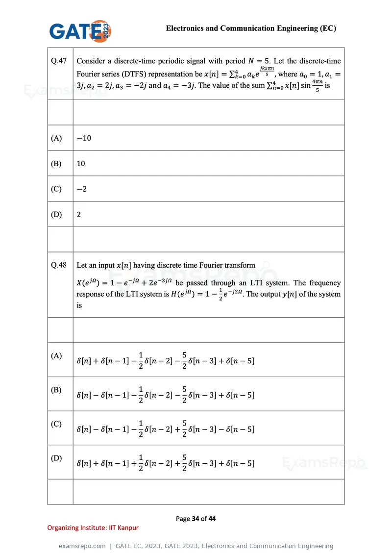
Text of page 34
Electronics and Communication Engineering (EC)


 Q.47     Consider a discrete-time periodic signal with period N = 5. Let the discrete-time
                                                                     jk2πn
          Fourier series (DTFS) representation be x[n] = ∑4k=0 ak e 5 , where a0 = 1, a1 =
                                                                                 4πn
          3j, a2 = 2j, a3 = −2j and a4 = −3j. The value of the sum ∑4n=0 x[n] sin 5 is


 (A)      −10


 (B)      10


 (C)      −2


 (D)      2


 Q.48     Let an input x[n] having discrete time Fourier transform

          X(e jΩ ) = 1 − e −jΩ + 2e −3jΩ be passed through an LTI system. The frequency
                                                       1
          response of the LTI system is H(e jΩ ) = 1 − 2 e −j2Ω . The output y[n] of the system
          is


 (A)                       1          5
          δ[n] + δ[n − 1] − δ[n − 2] − δ[n − 3] + δ[n − 5]
                           2          2

 (B)                       1          5
          δ[n] − δ[n − 1] − δ[n − 2] − δ[n − 3] + δ[n − 5]
                           2          2

 (C)                       1          5
          δ[n] − δ[n − 1] − δ[n − 2] + δ[n − 3] − δ[n − 5]
                           2          2

 (D)                       1          5
          δ[n] + δ[n − 1] + δ[n − 2] + δ[n − 3] + δ[n − 5]
                           2          2


                                         Page 34 of 44
Organizing Institute: IIT Kanpur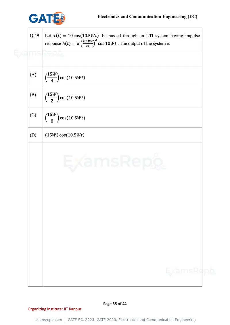
Text of page 35
Electronics and Communication Engineering (EC)


 Q.49     Let x(t) = 10 cos(10.5Wt) be passed through an LTI system having impulse
                                   sin Wt 2
          response ℎ(t) = π ( πt ) cos 10Wt . The output of the system is


 (A)       15W
          (    ) cos(10.5Wt)
            4


 (B)       15W
          (    ) cos(10.5Wt)
            2


 (C)       15W
          (    ) cos(10.5Wt)
            8


 (D)      (15W) cos(10.5Wt)


                                                Page 35 of 44
Organizing Institute: IIT Kanpur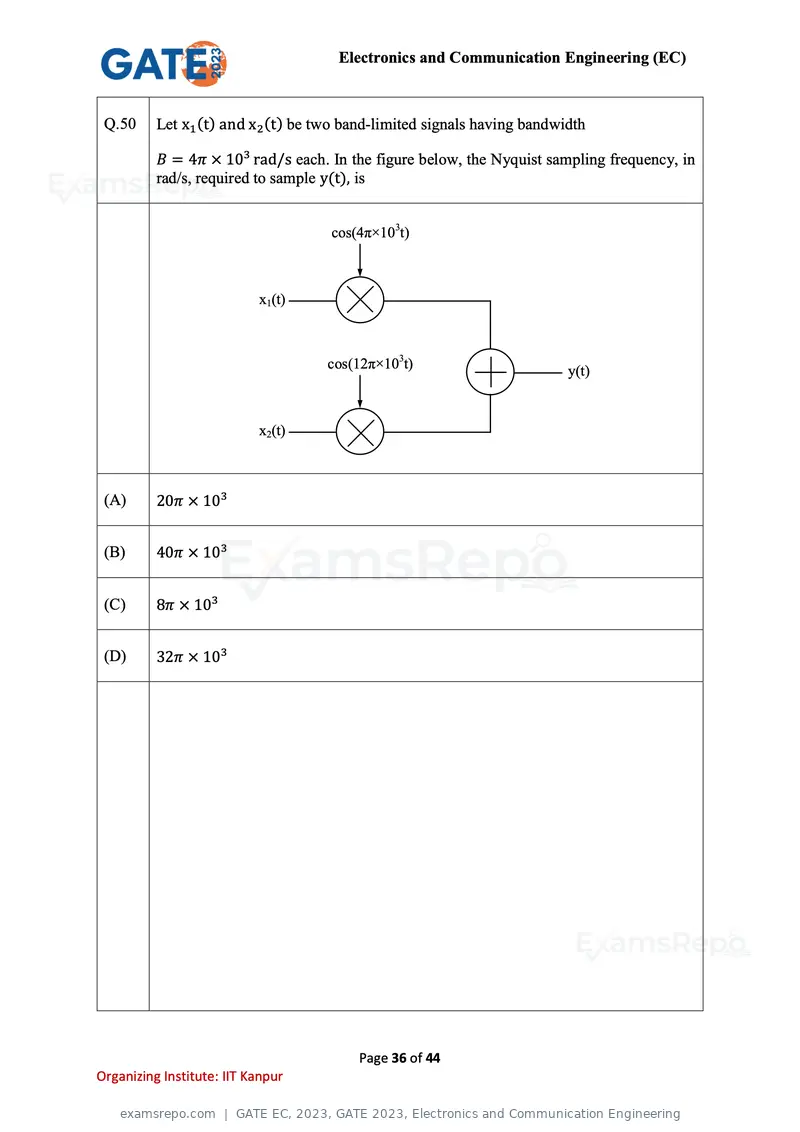
Text of page 36
Electronics and Communication Engineering (EC)


 Q.50     Let x1 (t) and x2 (t) be two band-limited signals having bandwidth

          B = 4π × 103 rad/s each. In the figure below, the Nyquist sampling frequency, in
          rad/s, required to sample y(t), is


                                    cos(4π×103t)


                           x1(t)


                                    cos(12π×103t)                        y(t)


                           x2(t)


 (A)      20π × 103


 (B)      40π × 103


 (C)      8π × 103


 (D)      32π × 103


                                         Page 36 of 44
Organizing Institute: IIT Kanpur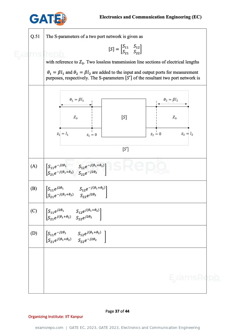
Text of page 37
Electronics and Communication Engineering (EC)


 Q.51     The S-parameters of a two port network is given as

                                                          S     S12
                                                   [S] = [ 11       ]
                                                          S21   S22

          with reference to Z0 . Two lossless transmission line sections of electrical lengths

           θ1 = βl1 and θ2 = βl2 are added to the input and output ports for measurement
          purposes, respectively. The S-parameters [S′] of the resultant two port network is


 (A)       S e −j2θ1         S12 e −j(θ1 +θ2 )
          [ 11 −j(θ +θ )                       ]
           S21 e   1  2      S22 e −j2θ2


 (B)       S e j2θ1          S12 e −j(θ1 +θ2 )
          [ 11 −j(θ +θ )                       ]
           S21 e    1 2      S22 e j2θ2


 (C)       S e j2θ1        S12 e j(θ1 +θ2 )
          [ 11 j(θ +θ )                     ]
           S21 e 1 2       S22 e j2θ2


 (D)       S e −j2θ1        S12 e j(θ1 +θ2 )
          [ 11 j(θ +θ )                      ]
           S21 e 1 2        S22 e −j2θ2


                                                Page 37 of 44
Organizing Institute: IIT Kanpur
Text of page 38
Electronics and Communication Engineering (EC)


 Q.52     The standing wave ratio on a 50 Ω lossless transmission line terminated in an
          unknown load impedance is found to be 2.0. The distance between successive
          voltage minima is 30 cm and the first minimum is located at 10 cm from the load.
          ZL can be replaced by an equivalent length lm and terminating resistance Rm of the
          same line. The value of Rm and lm , respectively, are


 (A)      Rm =100 Ω, lm = 20 cm


 (B)      Rm = 25 Ω, lm = 20 cm


 (C)      Rm =100 Ω, lm = 5 cm


 (D)      Rm = 25 Ω, lm = 5 cm


                                        Page 38 of 44
Organizing Institute: IIT Kanpur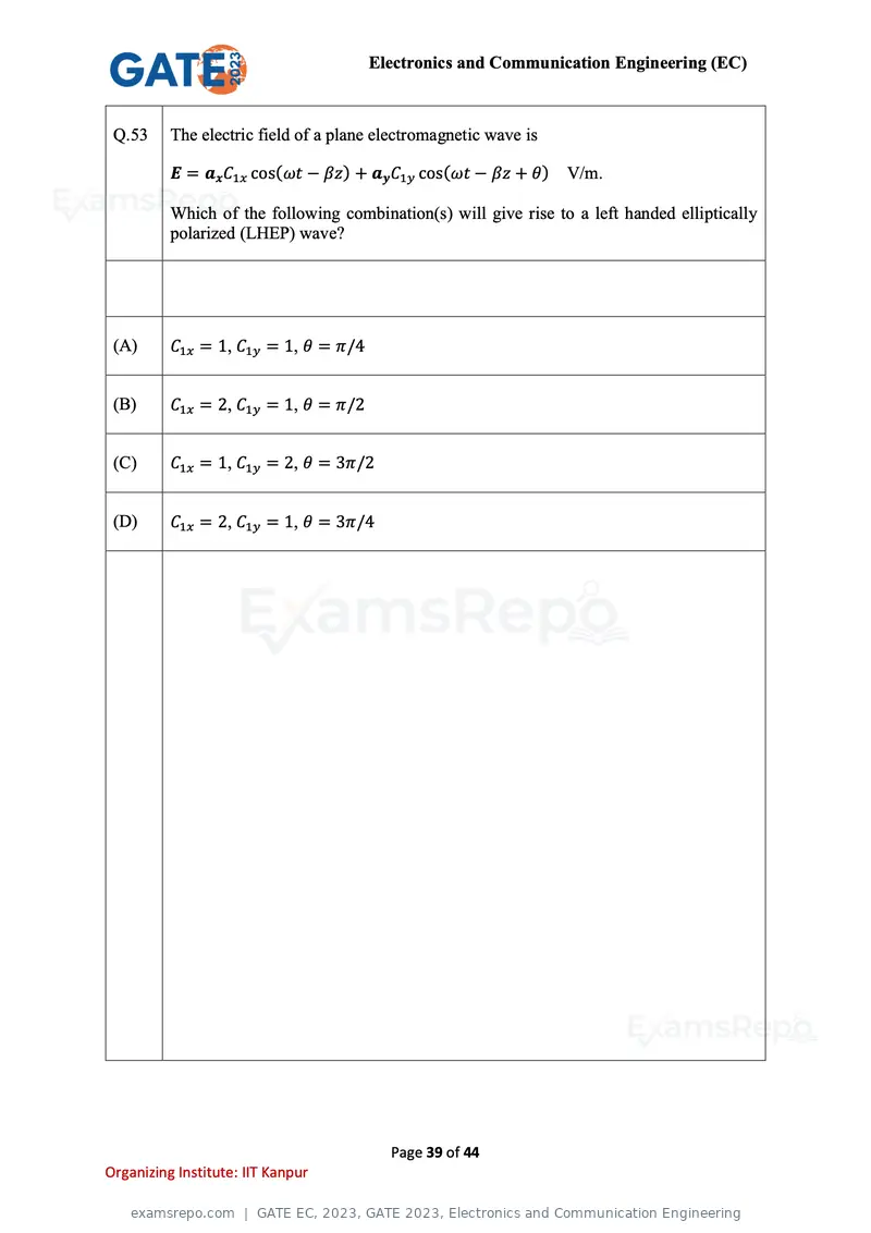
Text of page 39
Electronics and Communication Engineering (EC)


 Q.53     The electric field of a plane electromagnetic wave is

          E = ax C1x cos(ωt − βz) + ay C1y cos(ωt − βz + θ)       V/m.

          Which of the following combination(s) will give rise to a left handed elliptically
          polarized (LHEP) wave?


 (A)      C1x = 1, C1y = 1, θ = π/4


 (B)      C1x = 2, C1y = 1, θ = π/2


 (C)      C1x = 1, C1y = 2, θ = 3π/2


 (D)      C1x = 2, C1y = 1, θ = 3π/4


                                         Page 39 of 44
Organizing Institute: IIT Kanpur
Text of page 40
Electronics and Communication Engineering (EC)


 Q.54     The following circuit(s) representing a lumped element equivalent of an
          infinitesimal section of a transmission line is/are


 (A)                      LΔz        RΔz


                      CΔz/2                  GΔz/2


 (B)                          LΔz     RΔz


          GΔz           CΔz


 (C)                           LΔz     RΔz


          GΔz/2         CΔz/2              GΔz/2             CΔz/2


 (D)          RΔz/2     LΔz/2                        LΔz/2     RΔz/2


                                GΔz            CΔz


                                               Page 40 of 44
Organizing Institute: IIT Kanpur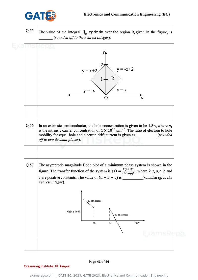
Text of page 41
Electronics and Communication Engineering (EC)


 Q.55     The value of the integral ∬R xy dx dy over the region R, given in the figure, is
          _______ (rounded off to the nearest integer).


                                                                y

                                                            2
                                              y = x+2                        y = -x+2

                                                            1            R

                                              y = -x                         y=x
                                                                O                                 x


 Q.56     In an extrinsic semiconductor, the hole concentration is given to be 1.5ni where ni
          is the intrinsic carrier concentration of 1 × 1010 cm−3. The ratio of electron to hole
          mobility for equal hole and electron drift current is given as __________ (rounded
          off to two decimal places).


 Q.57     The asymptotic magnitude Bode plot of a minimum phase system is shown in the
                                                               k(s+z)a
          figure. The transfer function of the system is (s) = b      c , where k, z, p, a, b and
                                                                                s (s+p)
          c are positive constants. The value of (a + b + c) is __________(rounded off to the
          nearest integer).


                                                -20 dB/decade


                             |G(jω )| in dB
                                                                         -40 dB/decade


                                                     ω1             ω2                    log ω


                                                 Page 41 of 44
Organizing Institute: IIT Kanpur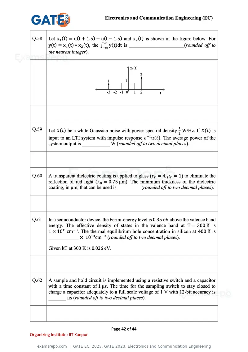
Text of page 42
Electronics and Communication Engineering (EC)


 Q.58     Let x1 (t) = u(t + 1.5) − u(t − 1.5) and x2 (t) is shown in the figure below. For
                                       ∞
          y(t) = x1 (t) ∗ x2 (t), the ∫−∞ y(t)dt is ______________________(rounded off to
          the nearest integer).


                                                       x2(t)
                                                               2
                                        1          1

                                        -3 -2 -1 0       1     2   t


 Q.59                                                                       1
          Let X(t) be a white Gaussian noise with power spectral density 2 W/Hz. If X(t) is
          input to an LTI system with impulse response e −t u(t). The average power of the
          system output is ___________ W (rounded off to two decimal places).


 Q.60     A transparent dielectric coating is applied to glass (εr = 4, μr = 1) to eliminate the
          reflection of red light (λ0 = 0.75 μm). The minimum thickness of the dielectric
          coating, in μm, that can be used is _________ (rounded off to two decimal places).


 Q.61     In a semiconductor device, the Fermi-energy level is 0.35 eV above the valence band
          energy. The effective density of states in the valence band at T = 300 K is
          1 × 1019 cm−3 . The thermal equilibrium hole concentration in silicon at 400 K is
          ____________ × 1013 cm−3 (rounded off to two decimal places).

          Given kT at 300 K is 0.026 eV.


 Q.62     A sample and hold circuit is implemented using a resistive switch and a capacitor
          with a time constant of 1 μs. The time for the sampling switch to stay closed to
          charge a capacitor adequately to a full scale voltage of 1 V with 12-bit accuracy is
          _______ μs (rounded off to two decimal places).


                                            Page 42 of 44
Organizing Institute: IIT Kanpur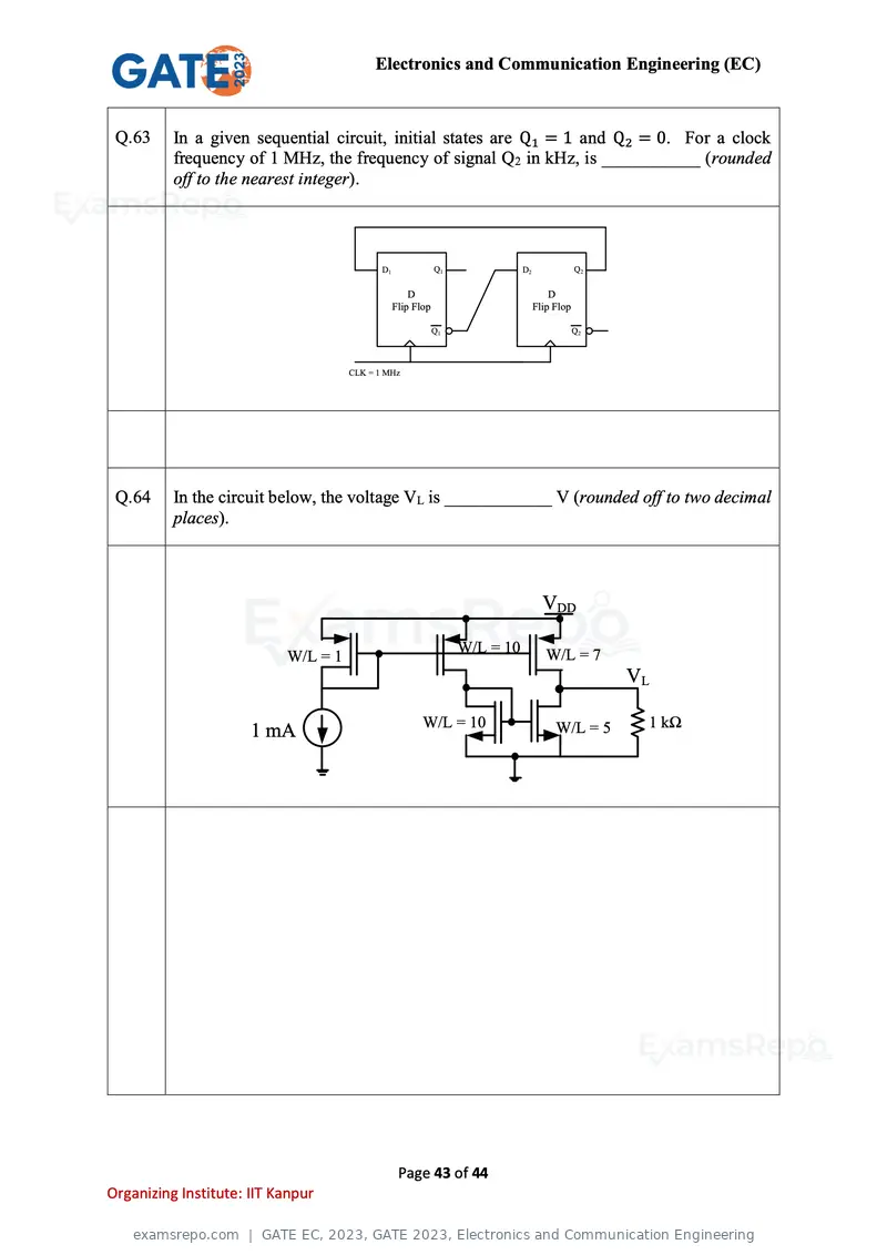
Text of page 43
Electronics and Communication Engineering (EC)


 Q.63     In a given sequential circuit, initial states are Q1 = 1 and Q2 = 0. For a clock
          frequency of 1 MHz, the frequency of signal Q2 in kHz, is ___________ (rounded
          off to the nearest integer).


                                            D1               Q1              D2               Q2

                                                     D                                D
                                                 Flip Flop                        Flip Flop

                                                             Q1                               Q2


                                     CLK = 1 MHz


 Q.64     In the circuit below, the voltage VL is ____________ V (rounded off to two decimal
          places).


                                                                                    VDD

                                                                  W/L = 10           W/L = 7
                           W/L = 1
                                                                                                   VL

                                                        W/L = 10                       W/L = 5      1 kΩ
                      1 mA


                                                  Page 43 of 44
Organizing Institute: IIT Kanpur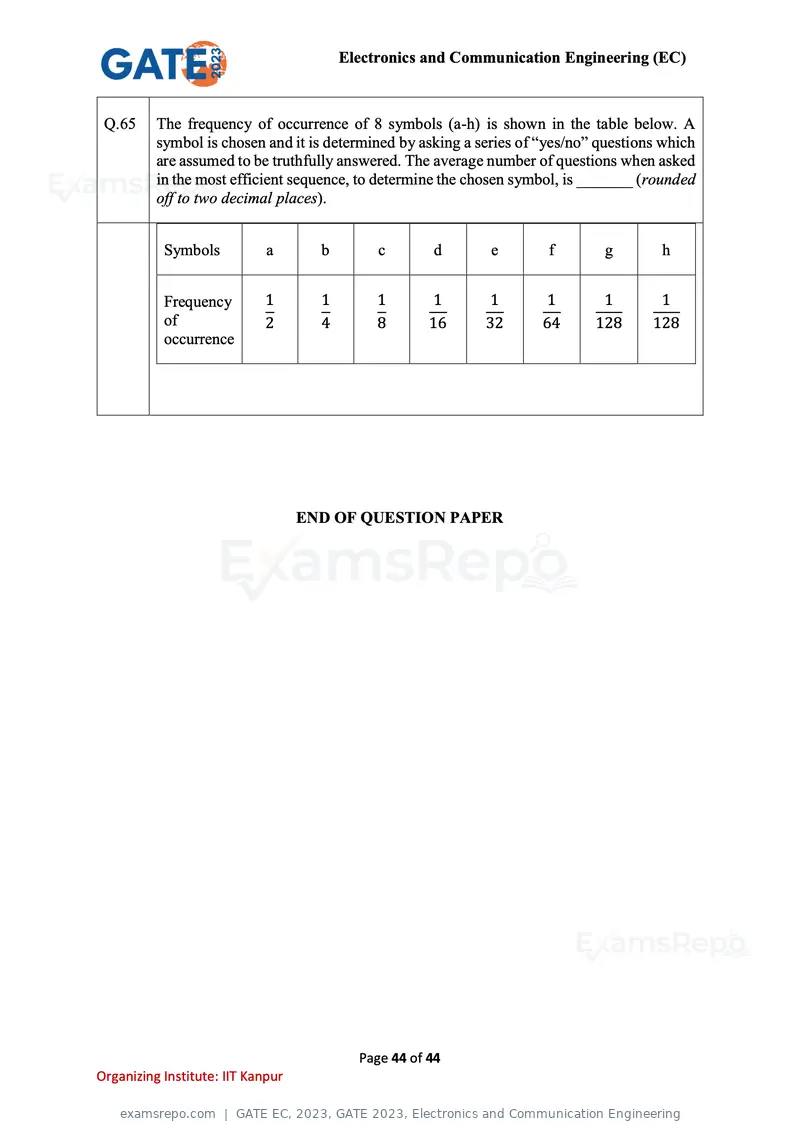
Text of page 44
Electronics and Communication Engineering (EC)


 Q.65     The frequency of occurrence of 8 symbols (a-h) is shown in the table below. A
          symbol is chosen and it is determined by asking a series of “yes/no” questions which
          are assumed to be truthfully answered. The average number of questions when asked
          in the most efficient sequence, to determine the chosen symbol, is _______ (rounded
          off to two decimal places).


              Symbols        a       b        c       d       e        f       g        h


              Frequency     1        1        1        1      1        1       1        1
              of            2        4        8       16     32       64      128      128
              occurrence


          .


                                   END OF QUESTION PAPER


                                           Page 44 of 44
Organizing Institute: IIT Kanpur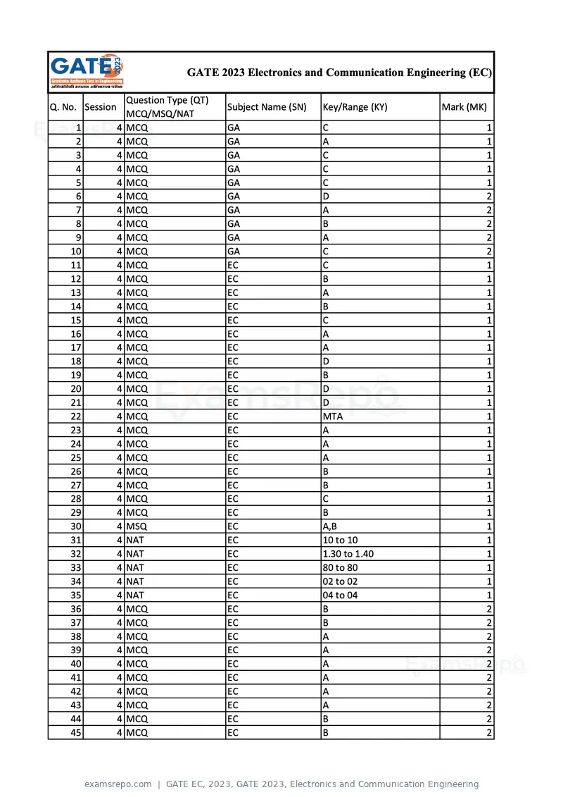
Text of page 1
GATE 2023 Electronics and Communication Engineering (EC)

                   Question Type (QT)
Q. No. Session                          Subject Name (SN)   Key/Range (KY)    Mark (MK)
                   MCQ/MSQ/NAT
     1           4 MCQ                  GA                  C                          1
     2           4 MCQ                  GA                  A                          1
     3           4 MCQ                  GA                  C                          1
     4           4 MCQ                  GA                  C                          1
     5           4 MCQ                  GA                  C                          1
     6           4 MCQ                  GA                  D                          2
     7           4 MCQ                  GA                  A                          2
     8           4 MCQ                  GA                  B                          2
     9           4 MCQ                  GA                  A                          2
    10           4 MCQ                  GA                  C                          2
    11           4 MCQ                  EC                  C                          1
    12           4 MCQ                  EC                  B                          1
    13           4 MCQ                  EC                  A                          1
    14           4 MCQ                  EC                  B                          1
    15           4 MCQ                  EC                  C                          1
    16           4 MCQ                  EC                  A                          1
    17           4 MCQ                  EC                  A                          1
    18           4 MCQ                  EC                  D                          1
    19           4 MCQ                  EC                  B                          1
    20           4 MCQ                  EC                  D                          1
    21           4 MCQ                  EC                  D                          1
    22           4 MCQ                  EC                  MTA                        1
    23           4 MCQ                  EC                  A                          1
    24           4 MCQ                  EC                  A                          1
    25           4 MCQ                  EC                  A                          1
    26           4 MCQ                  EC                  B                          1
    27           4 MCQ                  EC                  B                          1
    28           4 MCQ                  EC                  C                          1
    29           4 MCQ                  EC                  B                          1
    30           4 MSQ                  EC                  A,B                        1
    31           4 NAT                  EC                  10 to 10                   1
    32           4 NAT                  EC                  1.30 to 1.40               1
    33           4 NAT                  EC                  80 to 80                   1
    34           4 NAT                  EC                  02 to 02                   1
    35           4 NAT                  EC                  04 to 04                   1
    36           4 MCQ                  EC                  B                          2
    37           4 MCQ                  EC                  B                          2
    38           4 MCQ                  EC                  A                          2
    39           4 MCQ                  EC                  A                          2
    40           4 MCQ                  EC                  A                          2
    41           4 MCQ                  EC                  A                          2
    42           4 MCQ                  EC                  A                          2
    43           4 MCQ                  EC                  A                          2
    44           4 MCQ                  EC                  B                          2
    45           4 MCQ                  EC                  B                          2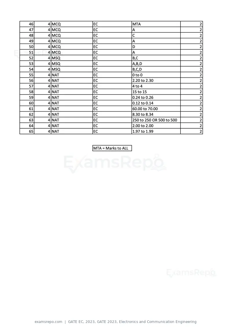
Text of page 2
46   4 MCQ   EC                   MTA                        2
47   4 MCQ   EC                   A                          2
48   4 MCQ   EC                   C                          2
49   4 MCQ   EC                   A                          2
50   4 MCQ   EC                   D                          2
51   4 MCQ   EC                   A                          2
52   4 MSQ   EC                   B,C                        2
53   4 MSQ   EC                   A,B,D                      2
54   4 MSQ   EC                   B,C,D                      2
55   4 NAT   EC                   0 to 0                     2
56   4 NAT   EC                   2.20 to 2.30               2
57   4 NAT   EC                   4 to 4                     2
58   4 NAT   EC                   15 to 15                   2
59   4 NAT   EC                   0.24 to 0.26               2
60   4 NAT   EC                   0.12 to 0.14               2
61   4 NAT   EC                   60.00 to 70.00             2
62   4 NAT   EC                   8.30 to 8.34               2
63   4 NAT   EC                   250 to 250 OR 500 to 500   2
64   4 NAT   EC                   2.00 to 2.00               2
65   4 NAT   EC                   1.97 to 1.99               2


             MTA = Marks to ALL
Page 1 of 44
Source: GATE. Question paper published by GATE.