
GATE EC 2024: Electronics and Communication Engineering
Text of page 1
Electronics and Communication Engineering (EC)


General Aptitude (GA)
Q.1 – Q.5 Carry ONE mark Each

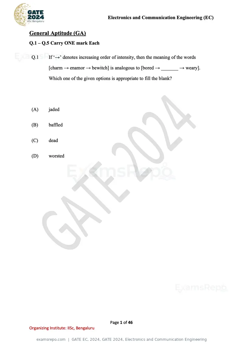
 Q.1       If ‘→’ denotes increasing order of intensity, then the meaning of the words

           [charm → enamor → bewitch] is analogous to [bored → _______ → weary].

           Which one of the given options is appropriate to fill the blank?


 (A)       jaded


 (B)       baffled


 (C)       dead


 (D)       worsted


                                          Page 1 of 46
Organizing Institute: IISc, Bengaluru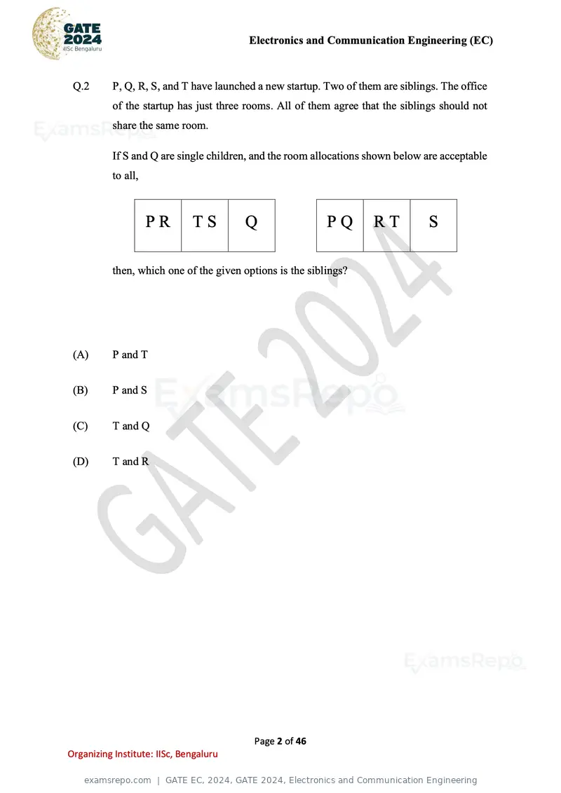
Text of page 2
Electronics and Communication Engineering (EC)


 Q.2       P, Q, R, S, and T have launched a new startup. Two of them are siblings. The office
           of the startup has just three rooms. All of them agree that the siblings should not
           share the same room.

           If S and Q are single children, and the room allocations shown below are acceptable
           to all,


                     PR       TS        Q                  PQ       RT           S

           then, which one of the given options is the siblings?


 (A)       P and T


 (B)       P and S


 (C)       T and Q


 (D)       T and R


                                           Page 2 of 46
Organizing Institute: IISc, Bengaluru
Text of page 3
Electronics and Communication Engineering (EC)


 Q.3       Five years ago, the ratio of Aman’s age to his father’s age was 1:4, and five years
           from now, the ratio will be 2:5. What was his father’s age when Aman was born?


 (A)       28 years


 (B)       30 years


 (C)       35 years


 (D)       32 years


 Q.4       For a real number x > 1,
                                          1       1       1
                                               +       +        =1
                                        log 2 x log 3 x log 4 x
           The value of x is


 (A)       4


 (B)       12


 (C)       24


 (D)       36


                                            Page 3 of 46
Organizing Institute: IISc, Bengaluru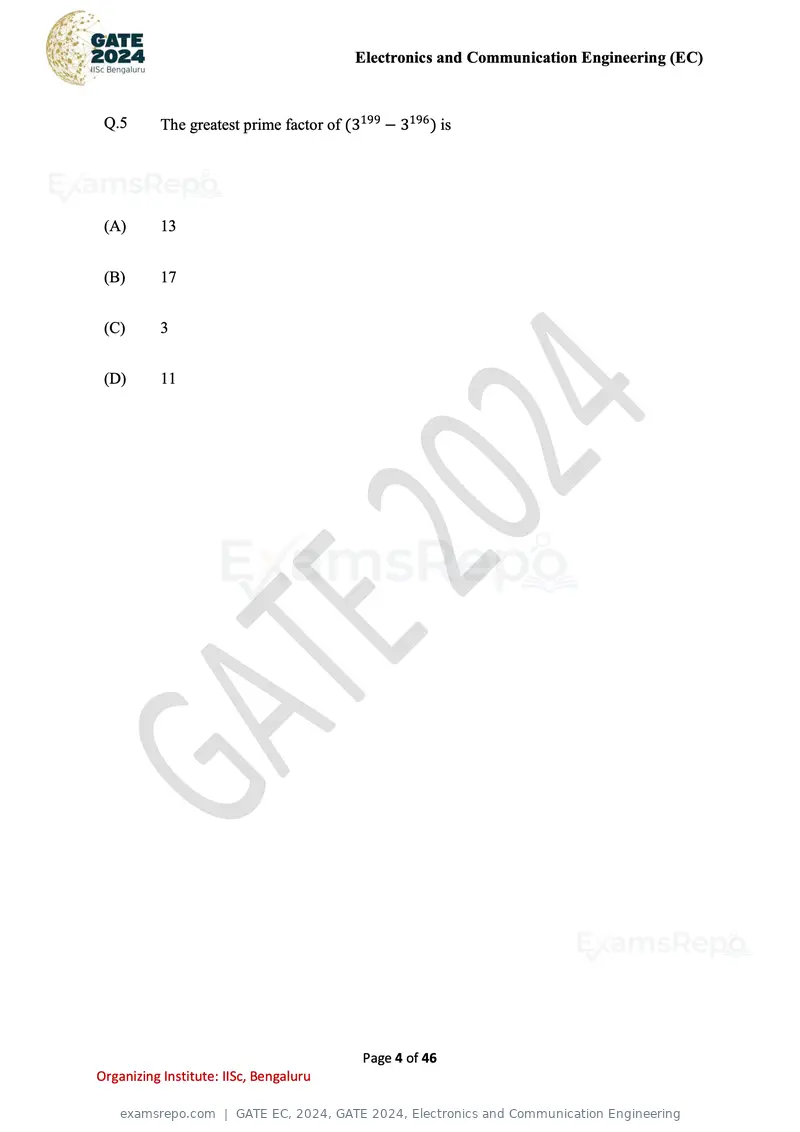
Text of page 4
Electronics and Communication Engineering (EC)


 Q.5       The greatest prime factor of (3199 − 3196 ) is


 (A)       13


 (B)       17


 (C)       3


 (D)       11


                                          Page 4 of 46
Organizing Institute: IISc, Bengaluru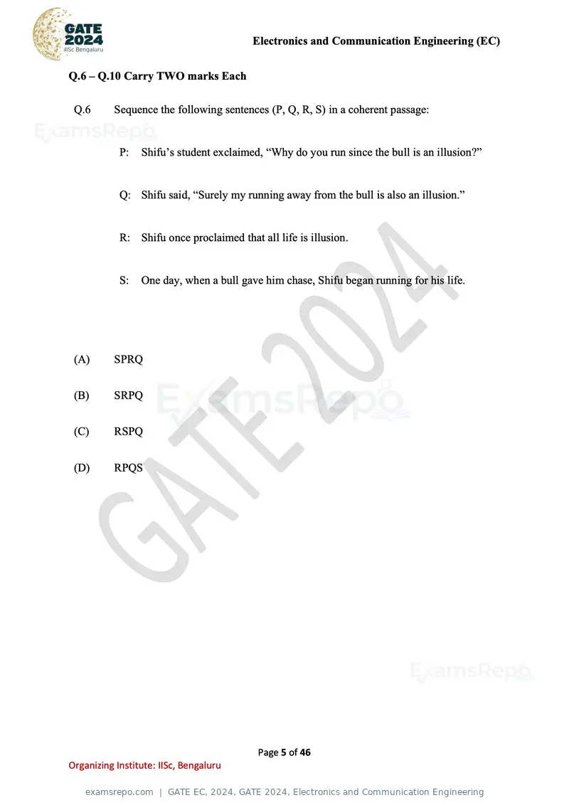
Text of page 5
Electronics and Communication Engineering (EC)


Q.6 – Q.10 Carry TWO marks Each

 Q.6       Sequence the following sentences (P, Q, R, S) in a coherent passage:


            P:   Shifu’s student exclaimed, “Why do you run since the bull is an illusion?”


            Q: Shifu said, “Surely my running away from the bull is also an illusion.”


            R: Shifu once proclaimed that all life is illusion.


            S:   One day, when a bull gave him chase, Shifu began running for his life.


 (A)       SPRQ


 (B)       SRPQ


 (C)       RSPQ


 (D)       RPQS


                                          Page 5 of 46
Organizing Institute: IISc, Bengaluru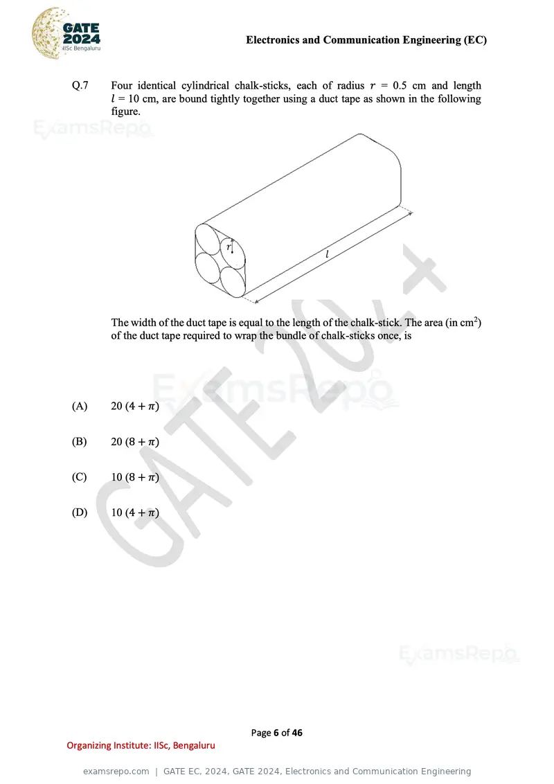
Text of page 6
Electronics and Communication Engineering (EC)


 Q.7       Four identical cylindrical chalk-sticks, each of radius r = 0.5 cm and length
           l = 10 cm, are bound tightly together using a duct tape as shown in the following
           figure.


           The width of the duct tape is equal to the length of the chalk-stick. The area (in cm2)
           of the duct tape required to wrap the bundle of chalk-sticks once, is


 (A)       20 (4 + π)


 (B)       20 (8 + π)


 (C)       10 (8 + π)


 (D)       10 (4 + π)


                                           Page 6 of 46
Organizing Institute: IISc, Bengaluru
Text of page 7
Electronics and Communication Engineering (EC)


 Q.8       The bar chart shows the data for the percentage of population falling into different
           categories based on Body Mass Index (BMI) in 2003 and 2023.

                                                                      2023    2003

                   Obese


              Overweight


                  Normal


            Underweight

                           0% 5% 10% 15% 20% 25% 30% 35% 40% 45% 50% 55%
                                          Percentage of population

           Based on the data provided, which one of the following options is INCORRECT?


 (A)       The ratio of the percentage of population falling into overweight category to the
           percentage of population falling into normal category has increased in 20 years.


 (B)       The ratio of the percentage of population falling into underweight category to the
           percentage of population falling into normal category has decreased in 20 years.


 (C)       The ratio of the percentage of population falling into obese category to the
           percentage of population falling into normal category has decreased in 20 years.


 (D)       The percentage of population falling into normal category has decreased in 20 years.


                                           Page 7 of 46
Organizing Institute: IISc, Bengaluru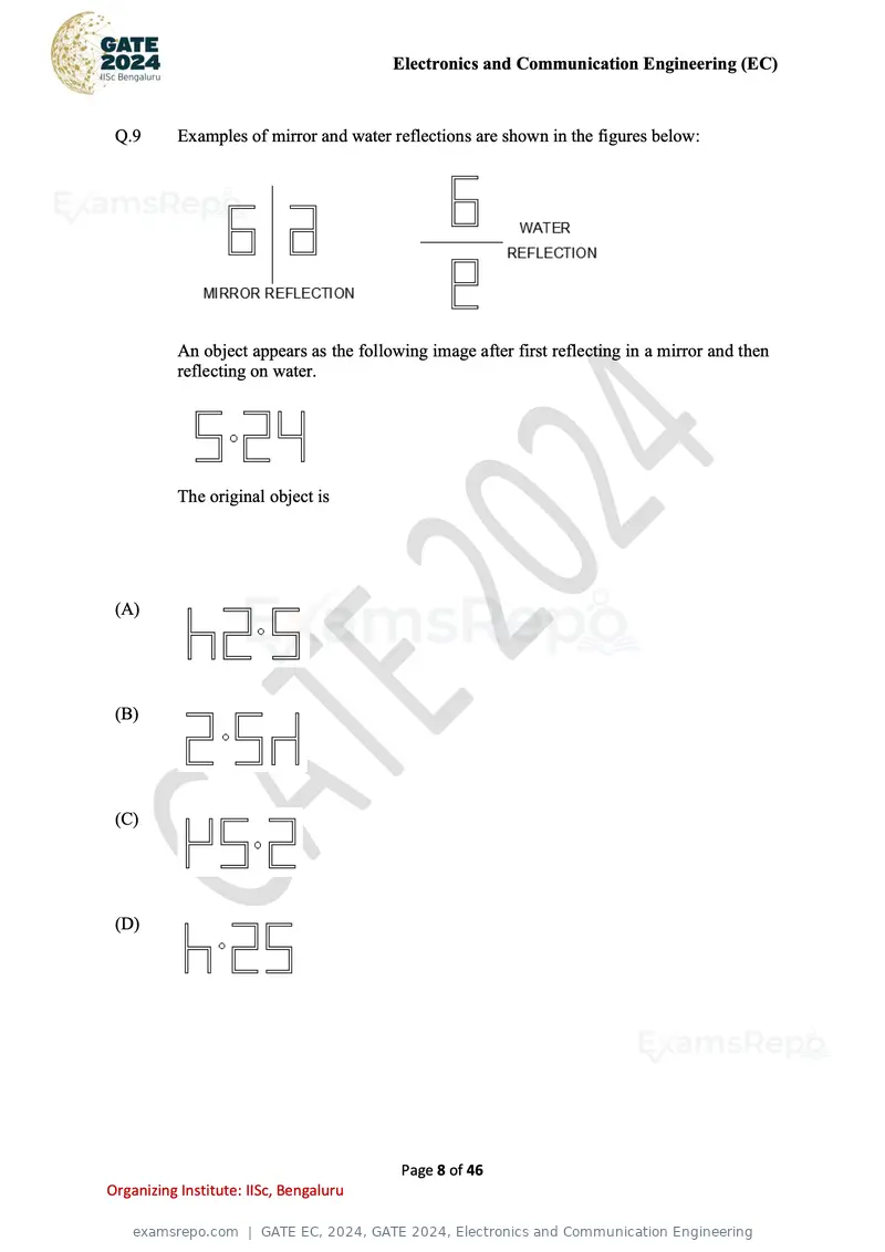
Text of page 8
Electronics and Communication Engineering (EC)


 Q.9       Examples of mirror and water reflections are shown in the figures below:


           An object appears as the following image after first reflecting in a mirror and then
           reflecting on water.


           The original object is


 (A)


 (B)


 (C)


 (D)


                                          Page 8 of 46
Organizing Institute: IISc, Bengaluru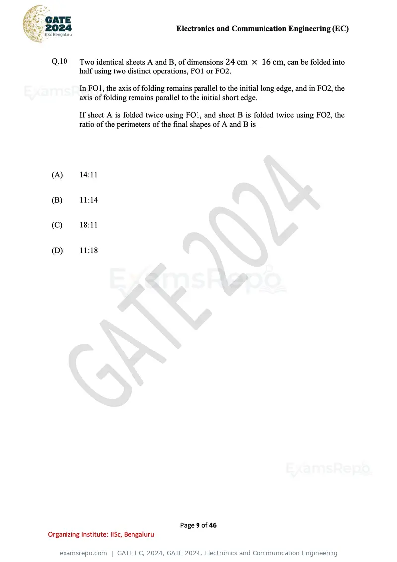
Text of page 9
Electronics and Communication Engineering (EC)


 Q.10      Two identical sheets A and B, of dimensions 24 cm × 16 cm, can be folded into
           half using two distinct operations, FO1 or FO2.

           In FO1, the axis of folding remains parallel to the initial long edge, and in FO2, the
           axis of folding remains parallel to the initial short edge.

           If sheet A is folded twice using FO1, and sheet B is folded twice using FO2, the
           ratio of the perimeters of the final shapes of A and B is


 (A)       14:11


 (B)       11:14


 (C)       18:11


 (D)       11:18


                                           Page 9 of 46
Organizing Institute: IISc, Bengaluru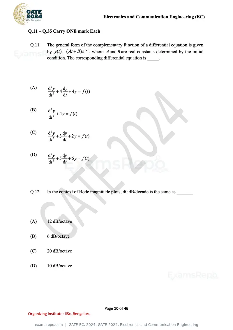
Text of page 10
Electronics and Communication Engineering (EC)


Q.11 – Q.35 Carry ONE mark Each

 Q.11      The general form of the complementary function of a differential equation is given
                                  −2 t
           by y (t ) = ( At + B) e , where A and B are real constants determined by the initial
           condition. The corresponding differential equation is _____.


 (A)       d2 y    dy
              2
                + 4 + 4 y = f (t )
           dt      dt


 (B)       d2 y
                + 4 y = f (t )
           dt 2


 (C)       d2 y    dy
              2
                + 3 + 2 y = f (t )
           dt      dt


 (D)       d2 y    dy
              2
                + 5 + 6 y = f (t )
           dt      dt


 Q.12      In the context of Bode magnitude plots, 40 dB/decade is the same as _______.


 (A)       12 dB/octave


 (B)       6 dB/octave


 (C)       20 dB/octave


 (D)       10 dB/octave


                                         Page 10 of 46
Organizing Institute: IISc, Bengaluru
Text of page 11
Electronics and Communication Engineering (EC)
6
Q.13 In the feedback control system shown in the figure below G ( s ) = .
s ( s + 1)( s + 2)
R (s) + E (s) Y ( s)
+ G(s)
-
R(s), Y (s), and E ( s) are the Laplace transforms of r (t ), y(t ), and e(t ) , respectively.
If the input r (t ) is a unit step function, then __________.
(A) lim e(t ) = 0
t →
(B) 1
lim e(t ) =
t→ 3
(C) 1
lim e(t ) =
t→ 4
(D) lim e(t ) does not exist, e(t ) is oscillatory
t→
Page 11 of 46
Organizing Institute: IISc, Bengaluru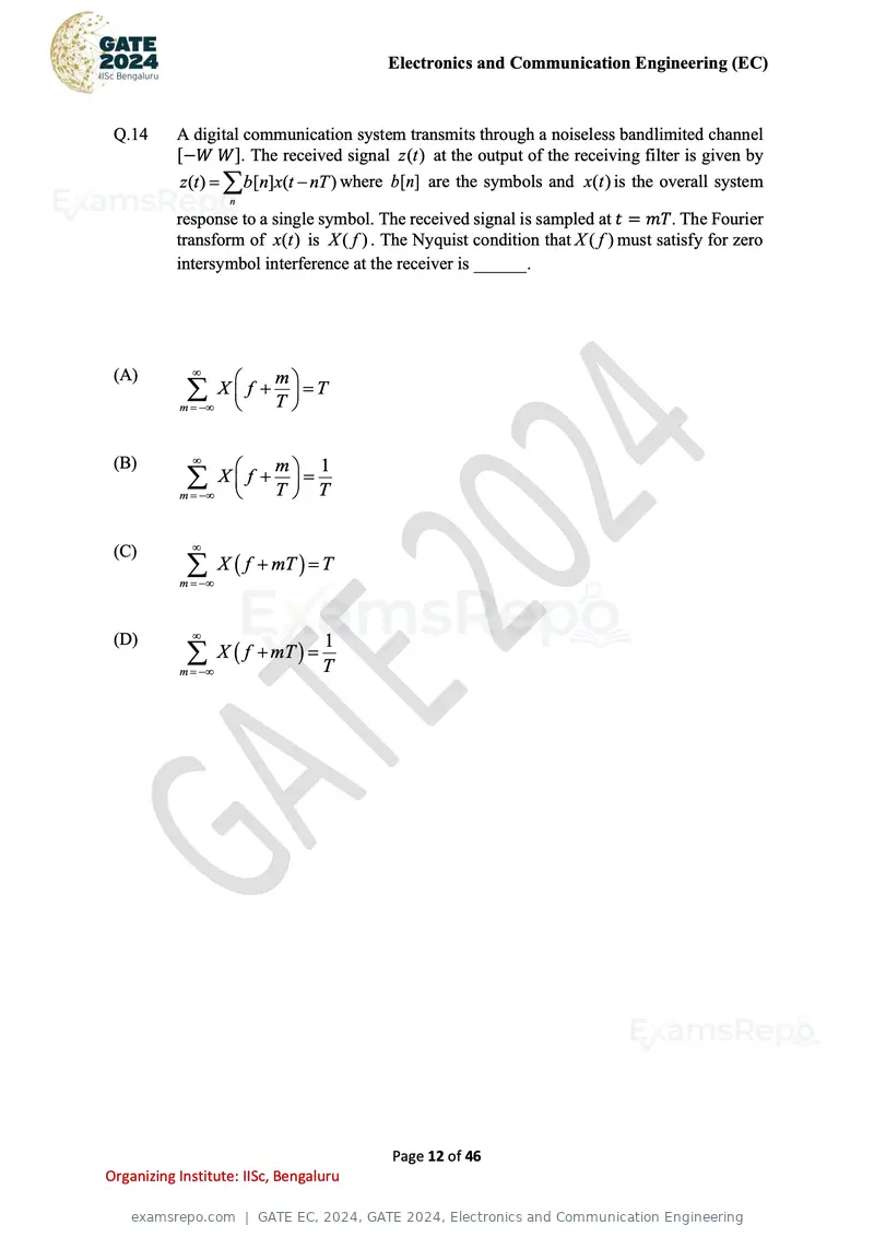
Text of page 12
Electronics and Communication Engineering (EC)
Q.14 A digital communication system transmits through a noiseless bandlimited channel
[−W W]. The received signal z (t ) at the output of the receiving filter is given by
z(t ) = b[n]x(t − nT ) where b [n] are the symbols and x(t ) is the overall system
n
response to a single symbol. The received signal is sampled at t = mT. The Fourier
transform of x(t ) is X ( f ) . The Nyquist condition that X ( f ) must satisfy for zero
intersymbol interference at the receiver is ______.
(A) m
X f + T = T
m = −
(B) m 1
X f + T = T
m = −
(C)
X ( f + mT ) = T
m = −
(D)
1
X ( f + mT ) = T
m = −
Page 12 of 46
Organizing Institute: IISc, Bengaluru
Text of page 14
Electronics and Communication Engineering (EC)


 Q.16      Let iˆ and ĵ be the unit vectors along x and y axes, respectively and let A be a
           positive constant. Which one of the following statements is true for the vector fields
                   ˆ + ˆjx) and F2 = A(iy
           F1 = A(iy                   ˆ − ˆjx) ?


 (A)       Both F1 and F2 are electrostatic fields.


 (B)       Only F1 is an electrostatic field.


 (C)       Only F2 is an electrostatic field.


 (D)       Neither F1 nor F2 is an electrostatic field.


                                           Page 14 of 46
Organizing Institute: IISc, Bengaluru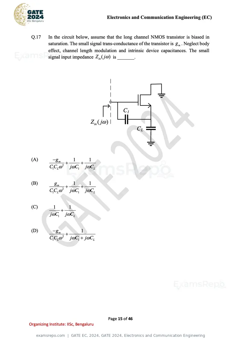
Text of page 15
Electronics and Communication Engineering (EC)
Q.17 In the circuit below, assume that the long channel NMOS transistor is biased in
saturation. The small signal trans-conductance of the transistor is g m . Neglect body
effect, channel length modulation and intrinsic device capacitances. The small
signal input impedance Z in ( j ) is _______.
C1
Z in ( j )
CL
(A) − gm 1 1
+ +
C1CL 2
jC1 jCL
(B) gm 1 1
+ +
C1CL 2
jC1 jCL
(C) 1 1
+
jC1 jCL
(D) − gm 1
+
C1CL 2
jC1 + jCL
Page 15 of 46
Organizing Institute: IISc, Bengaluru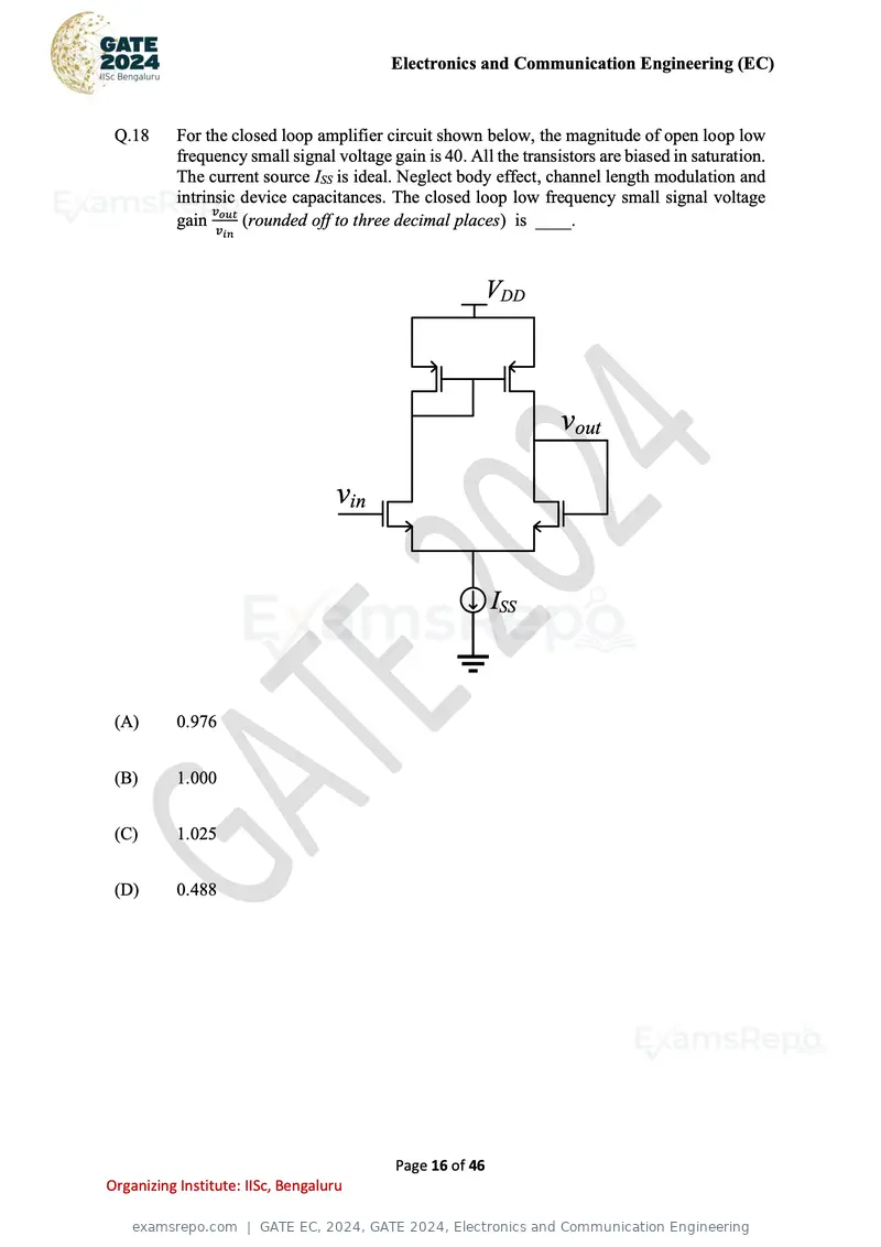
Text of page 16
Electronics and Communication Engineering (EC)


 Q.18      For the closed loop amplifier circuit shown below, the magnitude of open loop low
           frequency small signal voltage gain is 40. All the transistors are biased in saturation.
           The current source ISS is ideal. Neglect body effect, channel length modulation and
           intrinsic device capacitances. The closed loop low frequency small signal voltage
                 v
           gain vout (rounded off to three decimal places) is ____.
                   in


                                                         VDD


                                                                    vout

                                    vin


                                                           ISS


 (A)       0.976


 (B)       1.000


 (C)       1.025


 (D)       0.488


                                           Page 16 of 46
Organizing Institute: IISc, Bengaluru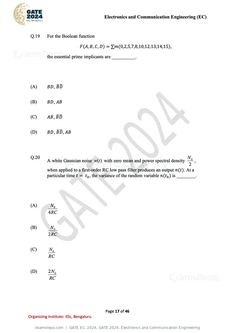
Text of page 17
Electronics and Communication Engineering (EC)


 Q.19      For the Boolean function

                              F(A, B, C, D) = ∑m(0,2,5,7,8,10,12,13,14,15),

           the essential prime implicants are __________.


 (A)       BD, B̅ D
                  ̅


 (B)       BD, AB


 (C)       AB, B̅ D
                  ̅


 (D)       BD, B̅ D
                  ̅ , AB


 Q.20                                                                                  N0
           A white Gaussian noise w(t ) with zero mean and power spectral density         ,
                                                                                       2
           when applied to a first-order RC low pass filter produces an output n(t). At a
           particular time t = tk , the variance of the random variable n(tk ) is ________.


 (A)        N0
           4 RC


 (B)        N0
           2 RC


 (C)       N0
           RC


 (D)       2N 0
           RC


                                          Page 17 of 46
Organizing Institute: IISc, Bengaluru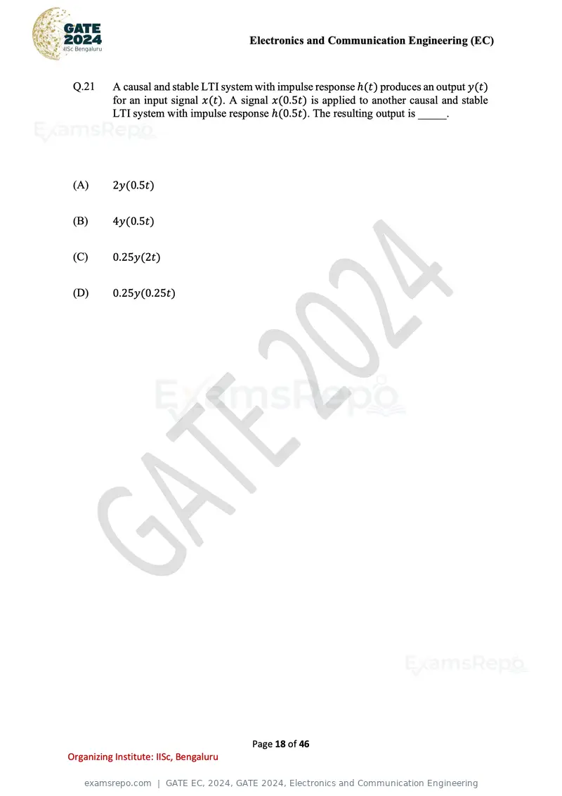
Text of page 18
Electronics and Communication Engineering (EC)


 Q.21      A causal and stable LTI system with impulse response ℎ(t) produces an output y(t)
           for an input signal x(t). A signal x(0.5t) is applied to another causal and stable
           LTI system with impulse response ℎ(0.5t). The resulting output is _____.


 (A)       2y(0.5t)


 (B)       4y(0.5t)


 (C)       0.25y(2t)


 (D)       0.25y(0.25t)


                                         Page 18 of 46
Organizing Institute: IISc, Bengaluru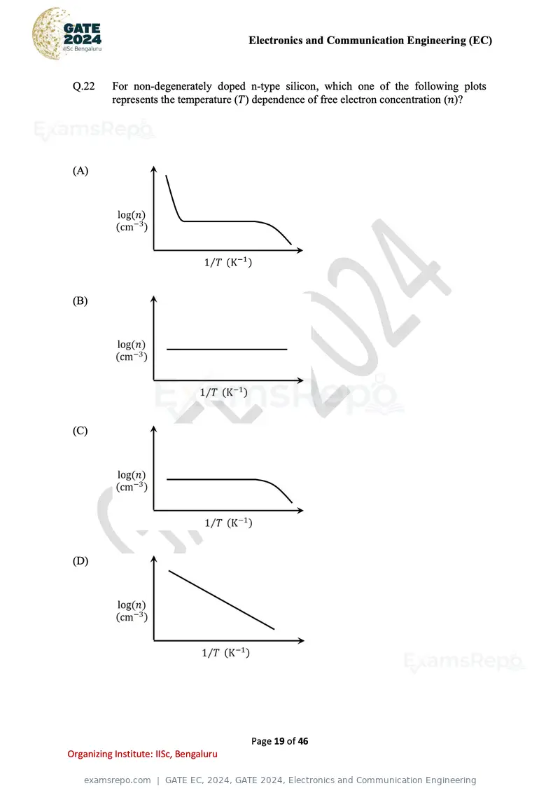
Text of page 19
Electronics and Communication Engineering (EC)


 Q.22      For non-degenerately doped n-type silicon, which one of the following plots
           represents the temperature (T) dependence of free electron concentration (n)?


 (A)


 (B)


 (C)


 (D)


                                        Page 19 of 46
Organizing Institute: IISc, Bengaluru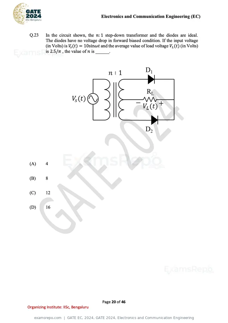
Text of page 20
Electronics and Communication Engineering (EC)


 Q.23      In the circuit shown, the n: 1 step-down transformer and the diodes are ideal.
           The diodes have no voltage drop in forward biased condition. If the input voltage
           (in Volts) is Vs (t) = 10sinωt and the average value of load voltage VL (t) (in Volts)
           is 2.5/π , the value of n is ______.


 (A)       4


 (B)       8


 (C)       12


 (D)       16


                                          Page 20 of 46
Organizing Institute: IISc, Bengaluru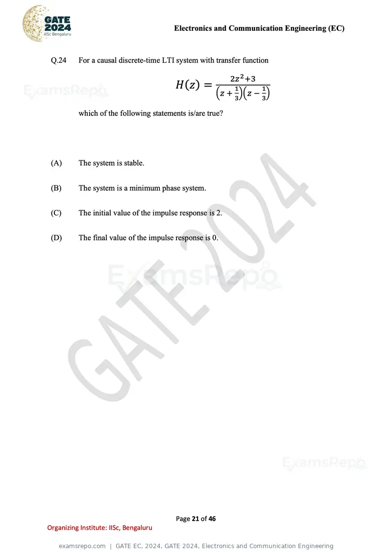
Text of page 21
Electronics and Communication Engineering (EC)


 Q.24      For a causal discrete-time LTI system with transfer function

                                                             2z 2 +3
                                          H (z) =             1        1
                                                       (z + )(z − )
                                                              3        3

           which of the following statements is/are true?


 (A)       The system is stable.


 (B)       The system is a minimum phase system.


 (C)       The initial value of the impulse response is 2.


 (D)       The final value of the impulse response is 0.


                                          Page 21 of 46
Organizing Institute: IISc, Bengaluru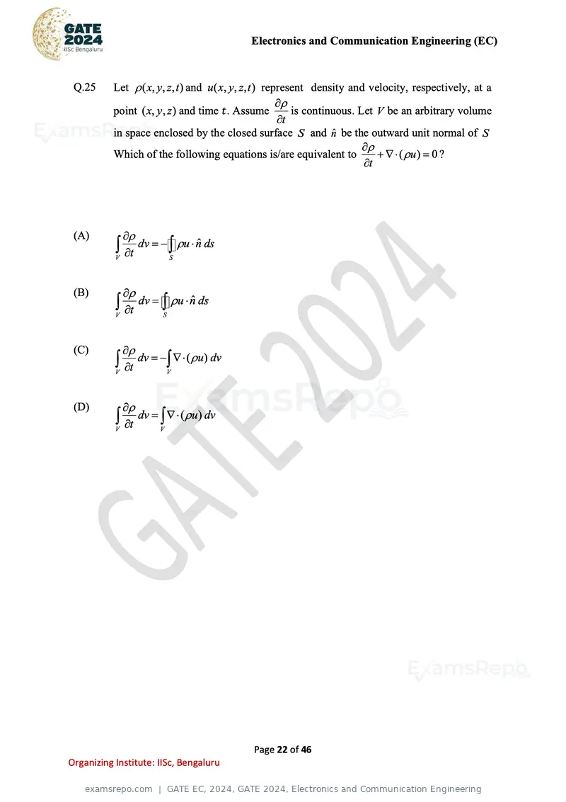
Text of page 22
Electronics and Communication Engineering (EC)
Q.25 Let ( x, y, z, t ) and u ( x, y, z, t ) represent density and velocity, respectively, at a
point ( x, y, z ) and time t. Assume is continuous. Let V be an arbitrary volume
t
in space enclosed by the closed surface S and n̂ be the outward unit normal of S
Which of the following equations is/are equivalent to + ( u) = 0 ?
t
(A)
t dv = − u nˆ ds
V S
(B)
t dv = u nˆ ds
V S
(C)
t dv = − (u) dv
V V
(D)
t dv = (u) dv
V V
Page 22 of 46
Organizing Institute: IISc, Bengaluru
Text of page 23
Electronics and Communication Engineering (EC)


 Q.26      The free electron concentration profile n(x) in a doped semiconductor at equilibrium
           is shown in the figure, where the points A, B, and C mark three different positions.
           Which of the following statements is/are true?


 (A)       For x between B and C, the electron diffusion current is directed from C to B.


 (B)       For x between B and A, the electron drift current is directed from B to A.


 (C)       For x between B and C, the electric field is directed from B to C.


 (D)       For x between B and A, the electric field is directed from A to B.


 Q.27      A machine has a 32-bit architecture with 1-word long instructions. It has 24 registers
           and supports an instruction set of size 40. Each instruction has five distinct fields,
           namely opcode, two source register identifiers, one destination register identifier,
           and an immediate value. Assuming that the immediate operand is an unsigned
           integer, its maximum value is ________.


                                          Page 23 of 46
Organizing Institute: IISc, Bengaluru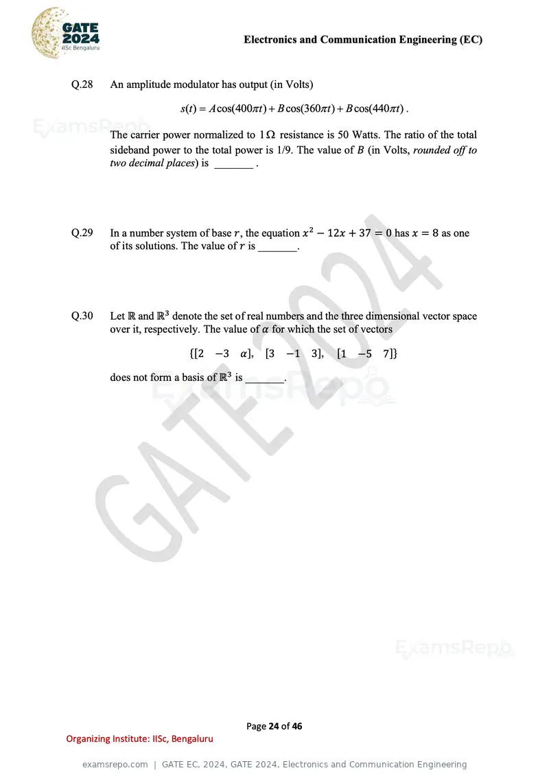
Text of page 24
Electronics and Communication Engineering (EC)
Q.28 An amplitude modulator has output (in Volts)
s(t ) = A cos(400 t ) + B cos(360 t ) + B cos(440 t ) .
The carrier power normalized to 1 resistance is 50 Watts. The ratio of the total
sideband power to the total power is 1/9. The value of B (in Volts, rounded off to
two decimal places) is _______ .
Q.29 In a number system of base r, the equation x 2 − 12x + 37 = 0 has x = 8 as one
of its solutions. The value of r is _______.
Q.30 Let ℝ and ℝ3 denote the set of real numbers and the three dimensional vector space
over it, respectively. The value of α for which the set of vectors
{[2 −3 α ], [3 −1 3], [1 −5 7]}
does not form a basis of ℝ3 is _______.
Page 24 of 46
Organizing Institute: IISc, Bengaluru
Text of page 25
Electronics and Communication Engineering (EC)
Q.31 In the given circuit, the current Ix (in mA) is ______.
1000 I0
- +
1k 1k 1k
5 mA
I0 Ix
2 mA
Q.32 In the circuit given below, the switch S was kept open for a sufficiently long time
and is closed at time t = 0. The time constant (in seconds) of the circuit for t > 0
is _______.
t=0
3H S
2 4 4
5A
Q.33 Suppose X and Y are independent and identically distributed random variables that
are distributed uniformly in the interval [0,1] . The probability that X Y
is _______ .
Page 25 of 46
Organizing Institute: IISc, Bengaluru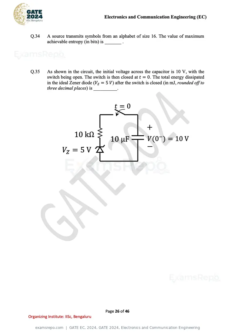
Text of page 26
Electronics and Communication Engineering (EC)


 Q.34      A source transmits symbols from an alphabet of size 16. The value of maximum
           achievable entropy (in bits) is _______ .


 Q.35      As shown in the circuit, the initial voltage across the capacitor is 10 V, with the
           switch being open. The switch is then closed at t = 0. The total energy dissipated
           in the ideal Zener diode (VZ = 5 V) after the switch is closed (in mJ, rounded off to
           three decimal places) is __________.


                                               t=0

                                                                +
                          10 kΩ                                  V(0− ) = 10 V
                                             10 μF
                   VZ = 5 V                                      −


                                          Page 26 of 46
Organizing Institute: IISc, Bengaluru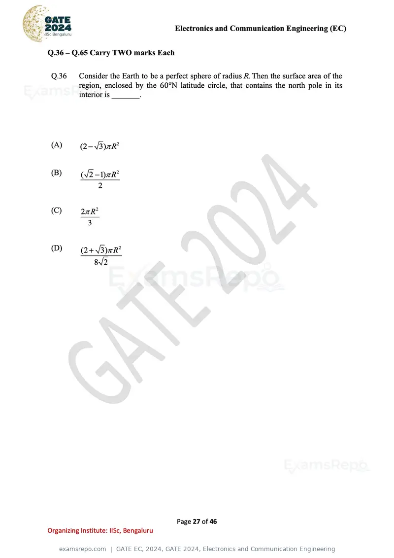
Text of page 27
Electronics and Communication Engineering (EC)
Q.36 – Q.65 Carry TWO marks Each
Q.36 Consider the Earth to be a perfect sphere of radius R. Then the surface area of the
region, enclosed by the 60°N latitude circle, that contains the north pole in its
interior is _______.
(A) (2 − 3) R2
(B) ( 2 − 1) R2
2
(C) 2 R 2
3
(D) (2 + 3) R 2
8 2
Page 27 of 46
Organizing Institute: IISc, Bengaluru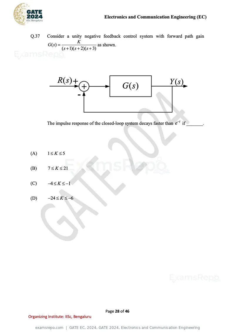
Text of page 28
Electronics and Communication Engineering (EC)
Q.37 Consider a unity negative feedback control system with forward path gain
K
G (s) = as shown.
( s + 1)( s + 2)( s + 3)
R( s ) + Y ( s)
+ G(s)
-
The impulse response of the closed-loop system decays faster than e−t if _______.
(A) 1 K 5
(B) 7 K 21
(C) −4 K −1
(D) −24 K −6
Page 28 of 46
Organizing Institute: IISc, Bengaluru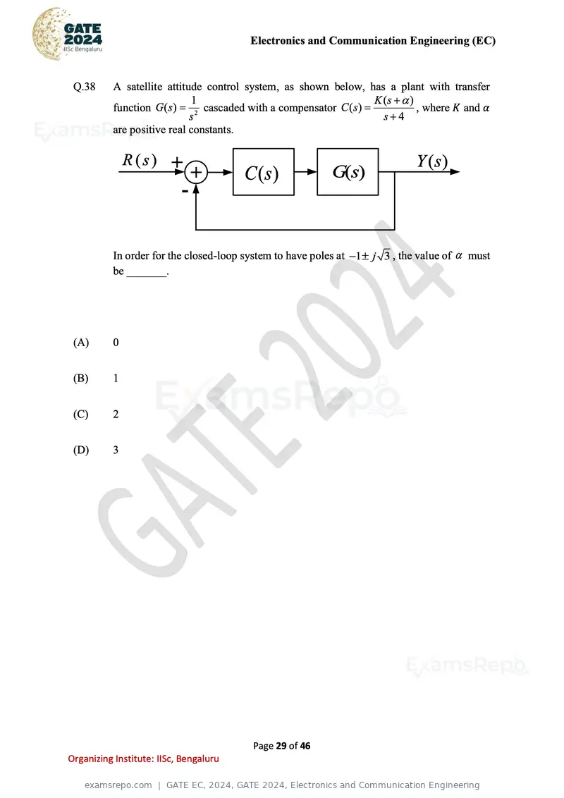
Text of page 29
Electronics and Communication Engineering (EC)
Q.38 A satellite attitude control system, as shown below, has a plant with transfer
1 K (s + )
function G ( s ) = 2 cascaded with a compensator C ( s ) = , where K and α
s s+4
are positive real constants.
R (s) + Y ( s)
+ C ( s) G(s)
-
In order for the closed-loop system to have poles at −1 j 3 , the value of must
be _______.
(A) 0
(B) 1
(C) 2
(D) 3
Page 29 of 46
Organizing Institute: IISc, Bengaluru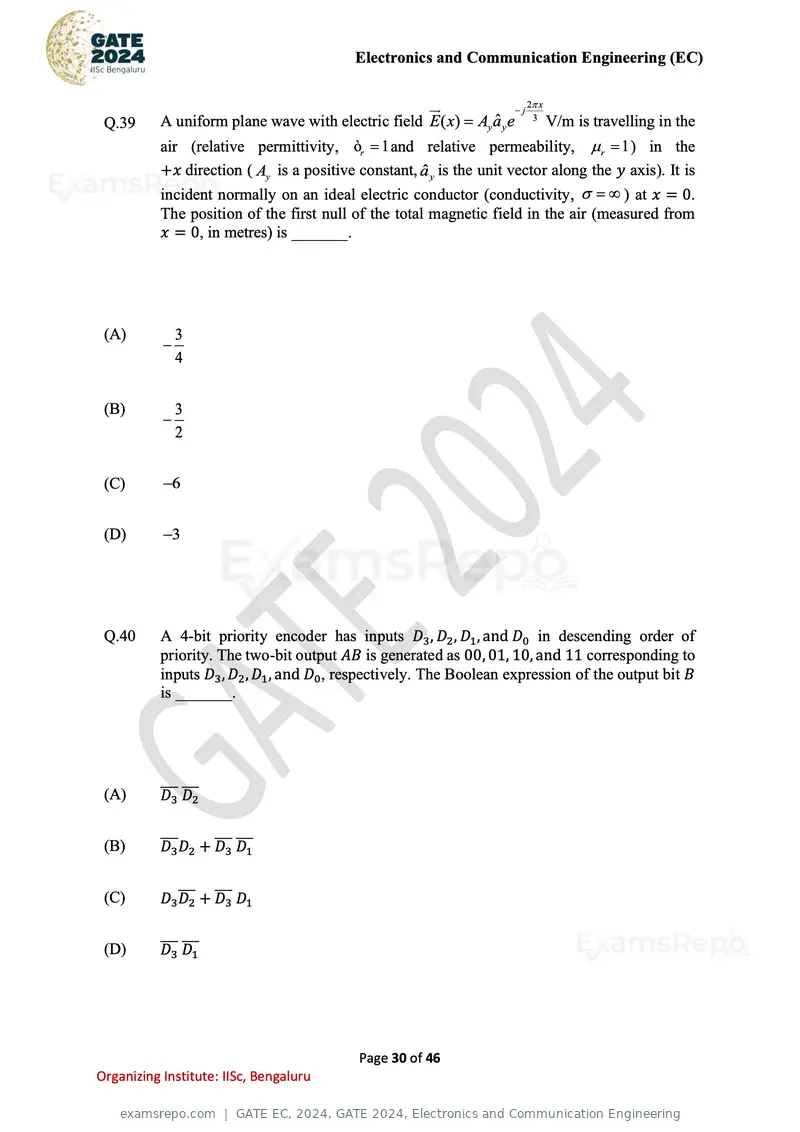
Text of page 30
Electronics and Communication Engineering (EC)
2 x
−j
Q.39 A uniform plane wave with electric field E ( x) = Ay aˆ y e 3
V/m is travelling in the
air (relative permittivity, òr = 1 and relative permeability, r = 1 ) in the
+x direction ( Ay is a positive constant, aˆ y is the unit vector along the y axis). It is
incident normally on an ideal electric conductor (conductivity, = ) at x = 0.
The position of the first null of the total magnetic field in the air (measured from
x = 0, in metres) is _______.
(A) 3
−
4
(B) 3
−
2
(C) −6
(D) −3
Q.40 A 4-bit priority encoder has inputs D3 , D2 , D1 , and D0 in descending order of
priority. The two-bit output AB is generated as 00, 01, 10, and 11 corresponding to
inputs D3 , D2 , D1 , and D0 , respectively. The Boolean expression of the output bit B
is _______.
(A) ̅̅̅3 D
D ̅̅̅2
(B) ̅̅̅
D3 D2 + ̅̅̅
D3 ̅̅̅
D1
(C) ̅̅̅2 + D
D3 D ̅̅̅3 D1
(D) ̅̅̅
D3 ̅̅̅
D1
Page 30 of 46
Organizing Institute: IISc, Bengaluru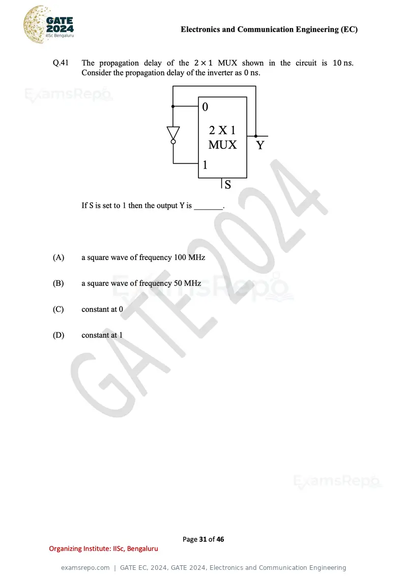
Text of page 31
Electronics and Communication Engineering (EC)


 Q.41      The propagation delay of the 2 × 1 MUX shown in the circuit is 10 ns.
           Consider the propagation delay of the inverter as 0 ns.


                                                 0
                                                     2X1
                                                     MUX       Y
                                                 1
                                                           S
           If S is set to 1 then the output Y is _______.


 (A)       a square wave of frequency 100 MHz


 (B)       a square wave of frequency 50 MHz


 (C)       constant at 0


 (D)       constant at 1


                                           Page 31 of 46
Organizing Institute: IISc, Bengaluru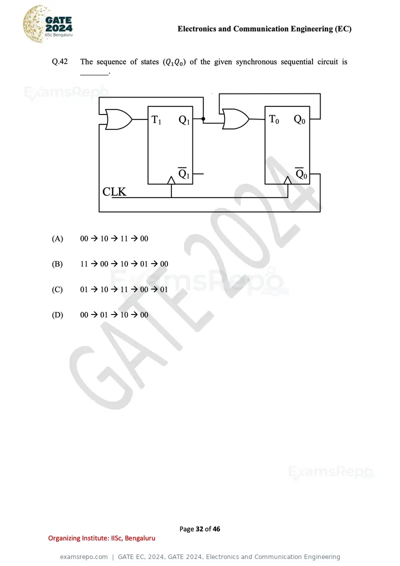
Text of page 32
Electronics and Communication Engineering (EC)


 Q.42      The sequence of states (Q1 Q0 ) of the given synchronous sequential circuit is
           _______.


                                   T1   Q1                        T0     Q0


                                        Q1                               Q0
                  CLK


 (A)       00 → 10 → 11 → 00


 (B)       11 → 00 → 10 → 01 → 00


 (C)       01 → 10 → 11 → 00 → 01


 (D)       00 → 01 → 10 → 00


                                        Page 32 of 46
Organizing Institute: IISc, Bengaluru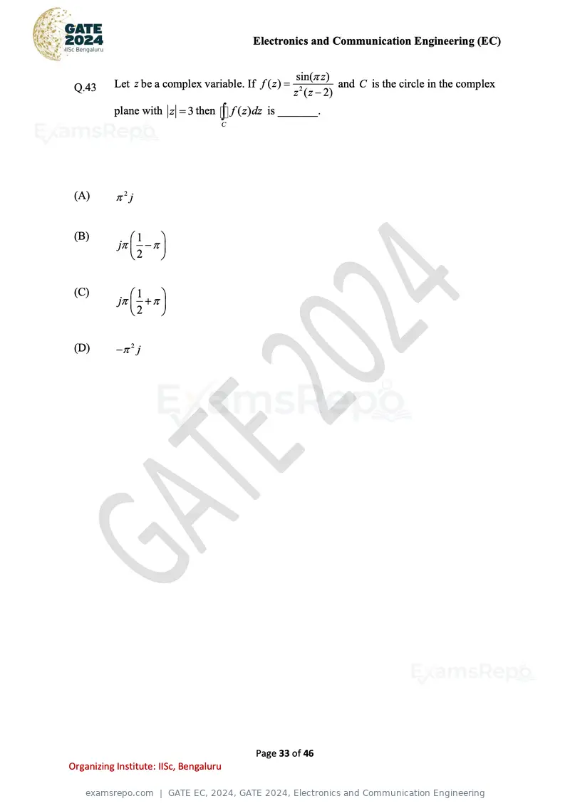
Text of page 33
Electronics and Communication Engineering (EC)
sin( z )
Q.43 Let z be a complex variable. If f ( z ) = and C is the circle in the complex
z 2 ( z − 2)
plane with z = 3 then f ( z )dz is _______.
C
(A) 2j
(B) 1
j −
2
(C) 1
j +
2
(D) − 2 j
Page 33 of 46
Organizing Institute: IISc, Bengaluru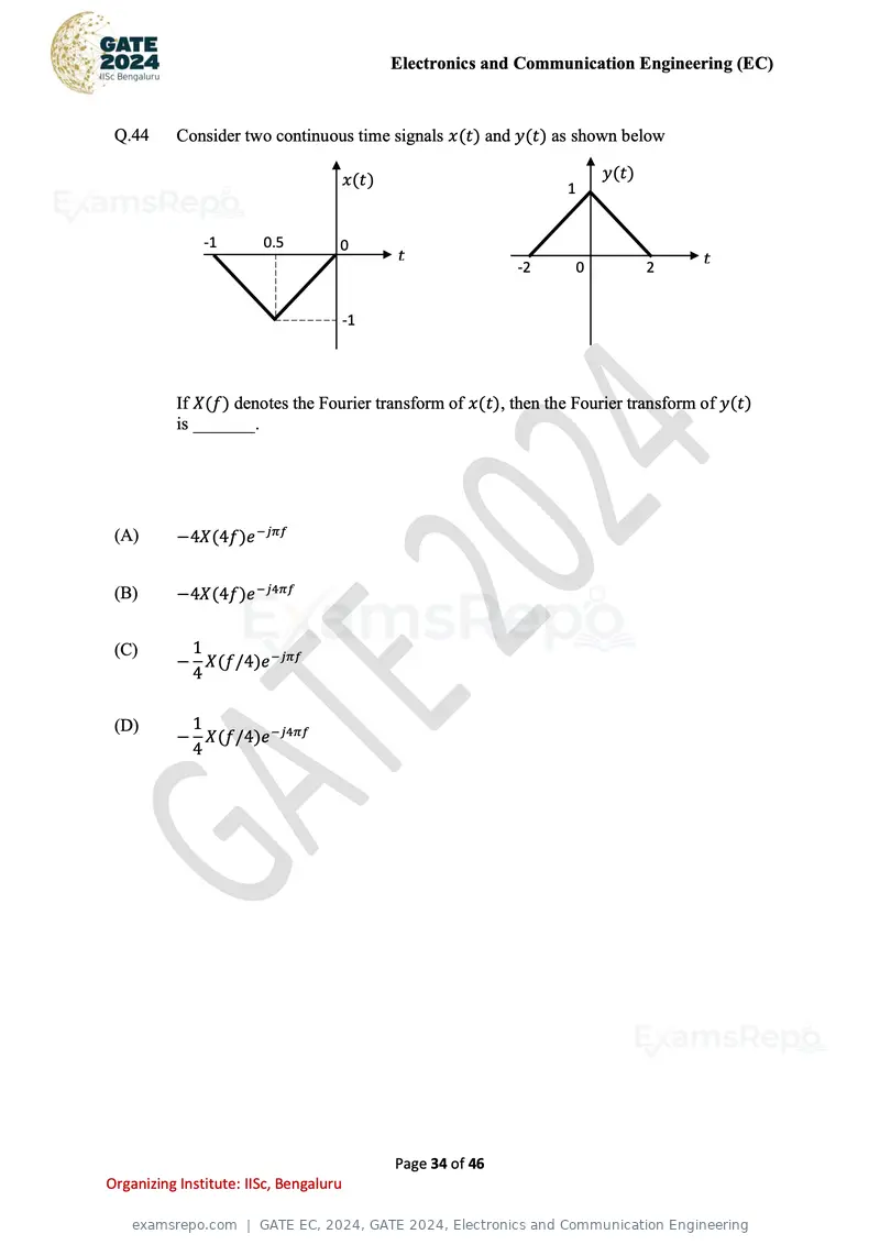
Text of page 34
Electronics and Communication Engineering (EC)


 Q.44      Consider two continuous time signals x(t) and y(t) as shown below

                                        x(t)                                y(t)
                                                                    1


               -1       0.5         0
                                               t                                       t
                                                               -2       0          2


                                        -1


           If X(f) denotes the Fourier transform of x(t), then the Fourier transform of y(t)
           is _______.


 (A)       −4X(4f)e −jπf


 (B)       −4X(4f)e −j4πf


 (C)        1
           − X(f/4)e −jπf
            4

 (D)        1
           − X(f/4)e −j4πf
            4


                                               Page 34 of 46
Organizing Institute: IISc, Bengaluru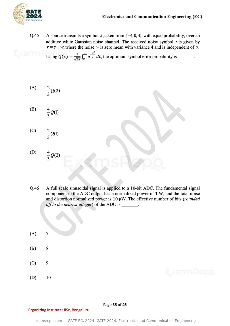
Text of page 35
Electronics and Communication Engineering (EC)


 Q.45      A source transmits a symbol s, taken from {−4,0, 4} with equal probability, over an
           additive white Gaussian noise channel. The received noisy symbol r is given by
           r = s + w, where the noise w is zero mean with variance 4 and is independent of s.
                                 ∞      −t2
                             1
           Using Q(x) =       ∫ e 2 dt, the optimum symbol error probability is _______.
                           √2π x


 (A)       2
             Q (2)
           3


 (B)       4
             Q(1)
           3


 (C)       2
             Q(1)
           3


 (D)       4
             Q (2)
           3


 Q.46      A full scale sinusoidal signal is applied to a 10-bit ADC. The fundamental signal
           component in the ADC output has a normalized power of 1 W, and the total noise
           and distortion normalized power is 10 μW. The effective number of bits (rounded
           off to the nearest integer) of the ADC is _______.


 (A)       7


 (B)       8


 (C)       9


 (D)       10


                                              Page 35 of 46
Organizing Institute: IISc, Bengaluru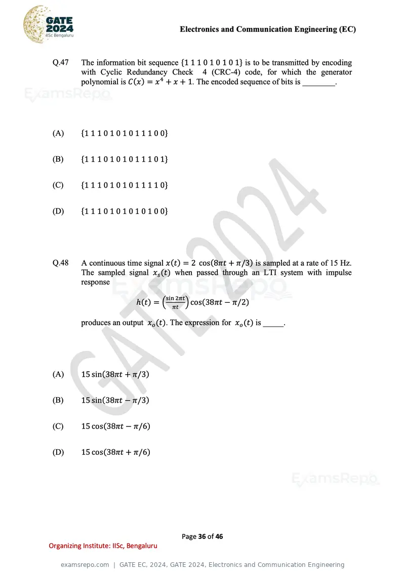
Text of page 36
Electronics and Communication Engineering (EC)


 Q.47      The information bit sequence {1 1 1 0 1 0 1 0 1} is to be transmitted by encoding
           with Cyclic Redundancy Check 4 (CRC-4) code, for which the generator
           polynomial is C(x) = x 4 + x + 1. The encoded sequence of bits is ________.


 (A)       {1 1 1 0 1 0 1 0 1 1 1 0 0}


 (B)       {1 1 1 0 1 0 1 0 1 1 1 0 1}


 (C)       {1 1 1 0 1 0 1 0 1 1 1 1 0}


 (D)       {1 1 1 0 1 0 1 0 1 0 1 0 0}


 Q.48      A continuous time signal x(t) = 2 cos(8πt + π/3) is sampled at a rate of 15 Hz.
           The sampled signal xs (t) when passed through an LTI system with impulse
           response
                                        sin 2πt
                             ℎ(t) = (             ) cos(38πt − π/2)
                                          πt

           produces an output xo (t). The expression for xo (t) is _____.


 (A)       15 sin(38πt + π/3)


 (B)       15 sin(38πt − π/3)


 (C)       15 cos(38πt − π/6)


 (D)       15 cos(38πt + π/6)


                                               Page 36 of 46
Organizing Institute: IISc, Bengaluru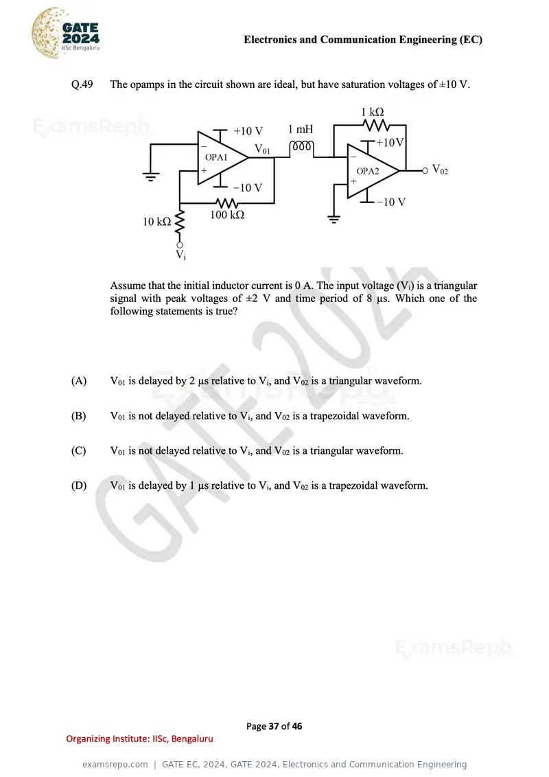
Text of page 37
Electronics and Communication Engineering (EC)


 Q.49      The opamps in the circuit shown are ideal, but have saturation voltages of ±10 V.


           Assume that the initial inductor current is 0 A. The input voltage (Vi) is a triangular
           signal with peak voltages of ±2 V and time period of 8 µs. Which one of the
           following statements is true?


 (A)       V01 is delayed by 2 µs relative to Vi, and V02 is a triangular waveform.


 (B)       V01 is not delayed relative to Vi, and V02 is a trapezoidal waveform.


 (C)       V01 is not delayed relative to Vi, and V02 is a triangular waveform.


 (D)       V01 is delayed by 1 µs relative to Vi, and V02 is a trapezoidal waveform.


                                           Page 37 of 46
Organizing Institute: IISc, Bengaluru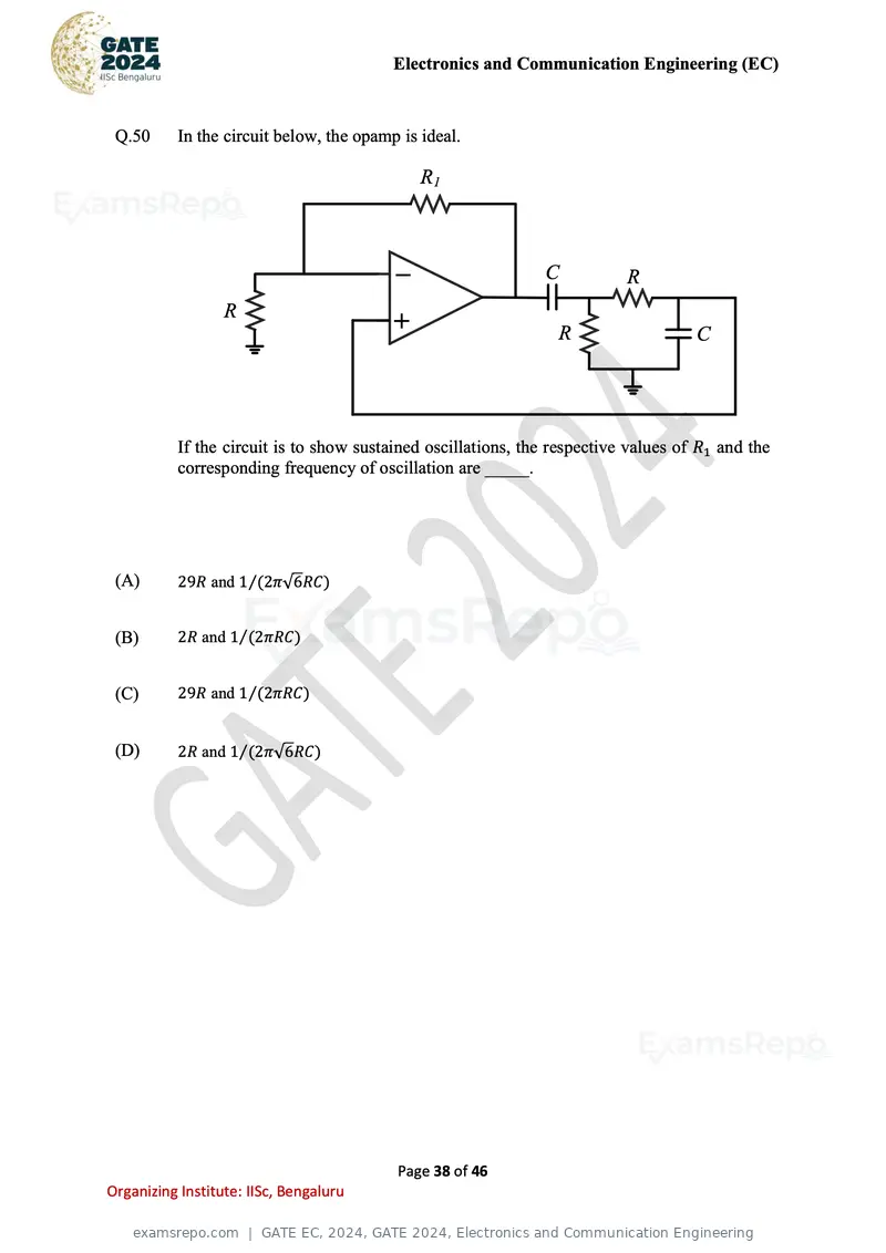
Text of page 38
Electronics and Communication Engineering (EC)


 Q.50      In the circuit below, the opamp is ideal.

                                              R1


                                          _                    C           R
                  R
                                          +                      R                   C


           If the circuit is to show sustained oscillations, the respective values of R1 and the
           corresponding frequency of oscillation are _____.


 (A)       29R and 1⁄(2π√6RC)


 (B)       2R and 1⁄(2πRC)


 (C)       29R and 1⁄(2πRC)


 (D)       2R and 1⁄(2π√6RC)


                                          Page 38 of 46
Organizing Institute: IISc, Bengaluru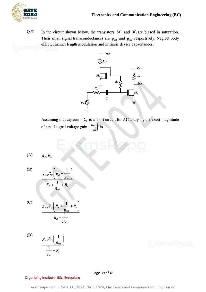
Text of page 39
Electronics and Communication Engineering (EC)
Q.51 In the circuit shown below, the transistors M 1 and M 2 are biased in saturation.
Their small signal transconductances are g m1 and g m 2 respectively. Neglect body
effect, channel length modulation and intrinsic device capacitances.
VDD
Iref
VDD
M1 RD
RB vout
RS
M2
C1
vin
Assuming that capacitor C1 is a short circuit for AC analysis, the exact magnitude
v
of small signal voltage gain | vout | is ______.
in
(A) g m 2 RD
(B) 1
g m 2 RD RB +
g m1
1
RB + + Rs
g m1
(C) 1
g m 2 RD RB + + Rs
g m1
1
RB +
g m1
(D) 1
g m 2 RD
g m1
1
+ Rs
g m1
Page 39 of 46
Organizing Institute: IISc, Bengaluru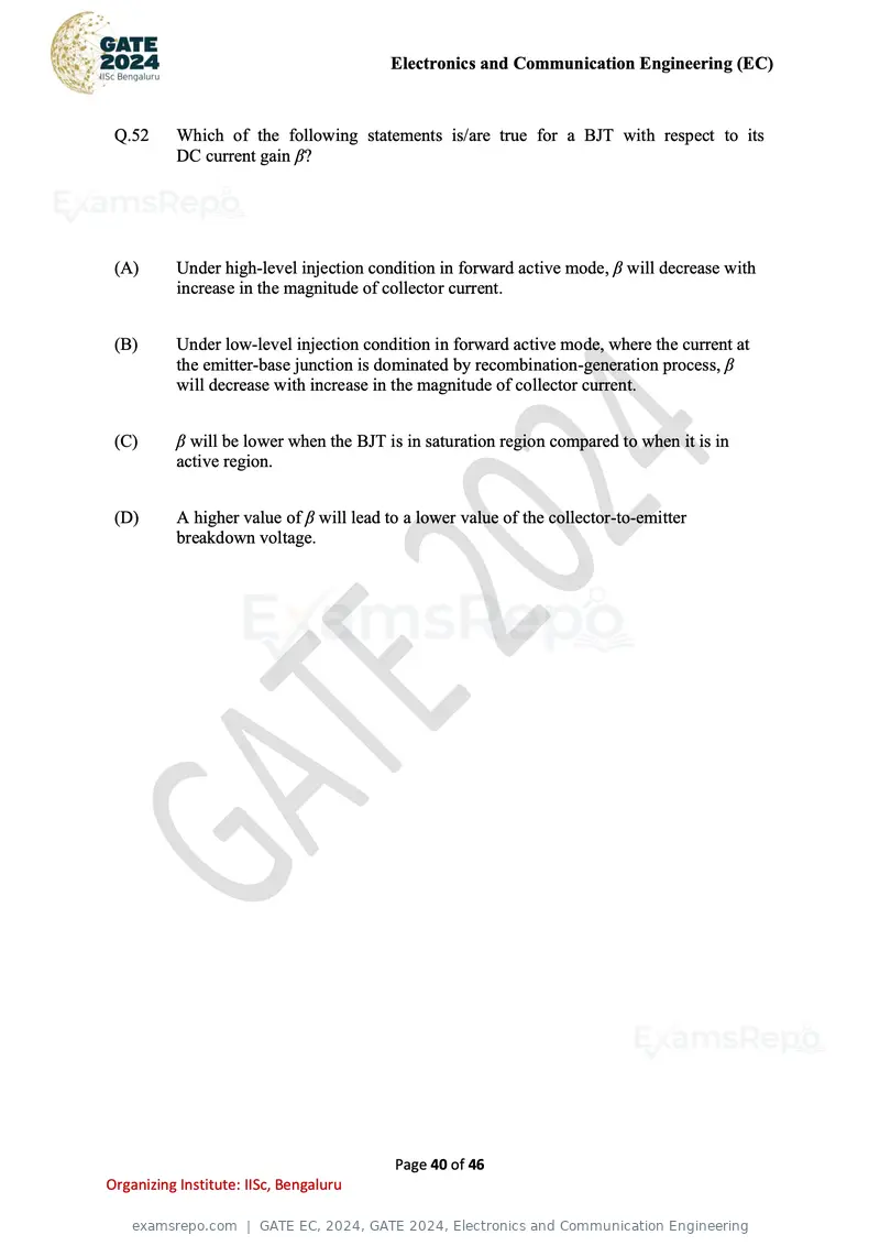
Text of page 40
Electronics and Communication Engineering (EC)


 Q.52      Which of the following statements is/are true for a BJT with respect to its
           DC current gain β?


 (A)       Under high-level injection condition in forward active mode, β will decrease with
           increase in the magnitude of collector current.


 (B)       Under low-level injection condition in forward active mode, where the current at
           the emitter-base junction is dominated by recombination-generation process, β
           will decrease with increase in the magnitude of collector current.


 (C)       β will be lower when the BJT is in saturation region compared to when it is in
           active region.


 (D)       A higher value of β will lead to a lower value of the collector-to-emitter
           breakdown voltage.


                                          Page 40 of 46
Organizing Institute: IISc, Bengaluru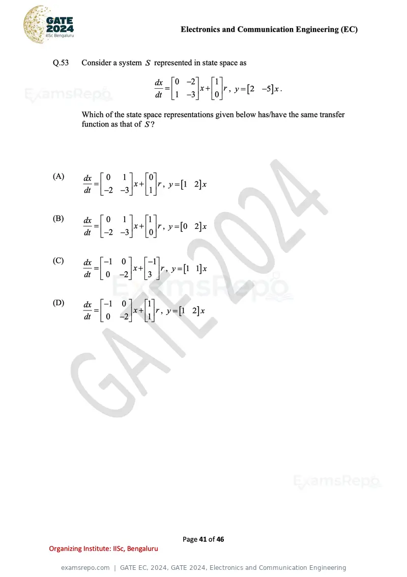
Text of page 41
Electronics and Communication Engineering (EC)
Q.53 Consider a system S represented in state space as
dx 0 −2 1
= x+ r , y = 2 −5 x .
dt 1 −3 0
Which of the state space representations given below has/have the same transfer
function as that of S ?
(A) dx 0 1 0
= x + r , y = 1 2 x
dt −2 −3 1
(B) dx 0 1 1
=
dt −2 −3
x + 0 r , y = 0 2 x
(C) dx −1 0 −1
= x+ r , y = 1 1 x
dt 0 −2 3
(D) dx −1 0 1
= x + r , y = 1 2 x
dt 0 −2 1
Page 41 of 46
Organizing Institute: IISc, Bengaluru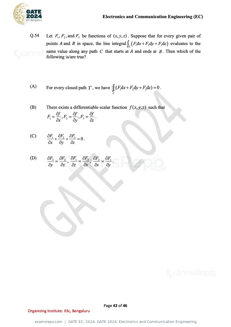
Text of page 42
Electronics and Communication Engineering (EC)
Q.54 Let F1 , F2 , and F3 be functions of ( x, y, z ) . Suppose that for every given pair of
points A and B in space, the line integral ( F1dx + F2 dy + F3dz ) evaluates to the
C
same value along any path C that starts at A and ends at B . Then which of the
following is/are true?
(A) For every closed path , we have ( F1dx + F2dy + F3dz ) = 0 .
(B) There exists a differentiable scalar function f ( x, y, z ) such that
f f f
F1 = , F2 = , F3 = .
x y z
(C) F1 F2 F3
+ + = 0.
x y z
(D) F3 F2 F1 F3 F2 F1
= , = , = .
y z z x x y
Page 42 of 46
Organizing Institute: IISc, Bengaluru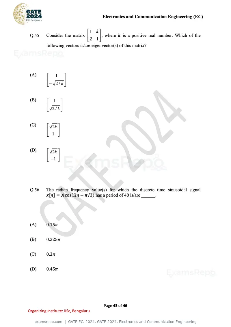
Text of page 43
Electronics and Communication Engineering (EC)
1 k
Q.55 Consider the matrix , where k is a positive real number. Which of the
2 1
following vectors is/are eigenvector(s) of this matrix?
(A) 1
− 2 / k
(B) 1
2/k
(C) 2k
1
(D) 2k
−1
Q.56 The radian frequency value(s) for which the discrete time sinusoidal signal
x[n] = A cos(Ωn + π/3) has a period of 40 is/are ______.
(A) 0.15π
(B) 0.225π
(C) 0.3π
(D) 0.45π
Page 43 of 46
Organizing Institute: IISc, Bengaluru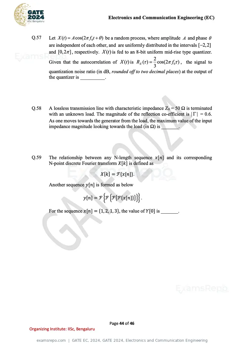
Text of page 44
Electronics and Communication Engineering (EC)
Q.57 Let X (t ) = A cos(2 f 0t + ) be a random process, where amplitude A and phase
are independent of each other, and are uniformly distributed in the intervals [−2, 2]
and [0, 2 ] , respectively. X (t ) is fed to an 8-bit uniform mid-rise type quantizer.
2
Given that the autocorrelation of X (t ) is RX ( ) = cos(2 f 0 ) , the signal to
3
quantization noise ratio (in dB, rounded off to two decimal places) at the output of
the quantizer is __________.
Q.58 A lossless transmission line with characteristic impedance Z0 = 50 Ω is terminated
with an unknown load. The magnitude of the reflection co-efficient is | | = 0.6.
As one moves towards the generator from the load, the maximum value of the input
impedance magnitude looking towards the load (in Ω) is _______.
Q.59 The relationship between any N-length sequence x[n] and its corresponding
N-point discrete Fourier transform X[k] is defined as
X[k] = ℱ{x[n]}.
Another sequence y[n] is formed as below
y[n] = ℱ {ℱ {ℱ{ℱ{x[n]}}}} .
For the sequence x[n] = {1, 2, 1, 3}, the value of Y[0] is _______.
Page 44 of 46
Organizing Institute: IISc, Bengaluru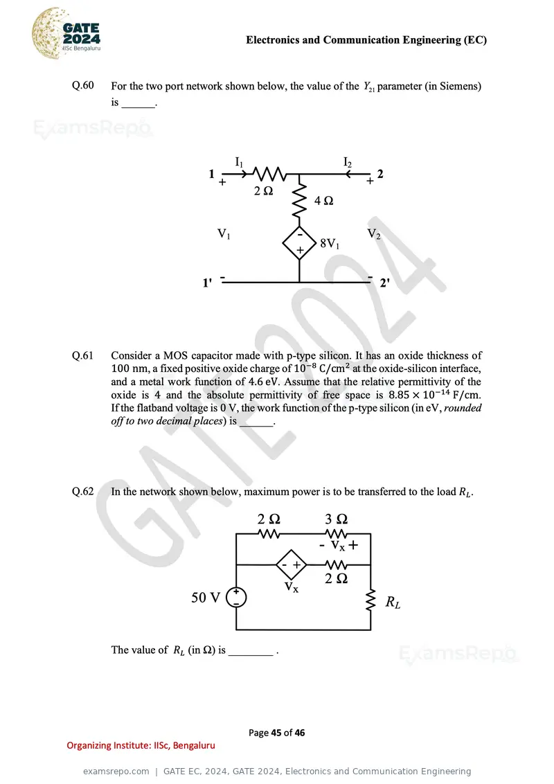
Text of page 45
Electronics and Communication Engineering (EC)


 Q.60      For the two port network shown below, the value of the Y21 parameter (in Siemens)
           is ______.


                                             I1                           I2
                                   1                                               2
                                        +                                      +
                                                   2
                                                                  4

                                        V1                   -                 V2
                                                                  8V1
                                                             +

                                 1' -                                          - 2'


 Q.61      Consider a MOS capacitor made with p-type silicon. It has an oxide thickness of
           100 nm, a fixed positive oxide charge of 10−8 C/cm2 at the oxide-silicon interface,
           and a metal work function of 4.6 eV. Assume that the relative permittivity of the
           oxide is 4 and the absolute permittivity of free space is 8.85 × 10⁻¹⁴ F/cm.
           If the flatband voltage is 0 V, the work function of the p-type silicon (in eV, rounded
           off to two decimal places) is ______.


 Q.62      In the network shown below, maximum power is to be transferred to the load RL .

                                                    2                 3
                                                                  - vx +
                                                         - +
                                                          vx          2
                              50 V                                                     RL


           The value of RL (in Ω) is ________ .


                                                  Page 45 of 46
Organizing Institute: IISc, Bengaluru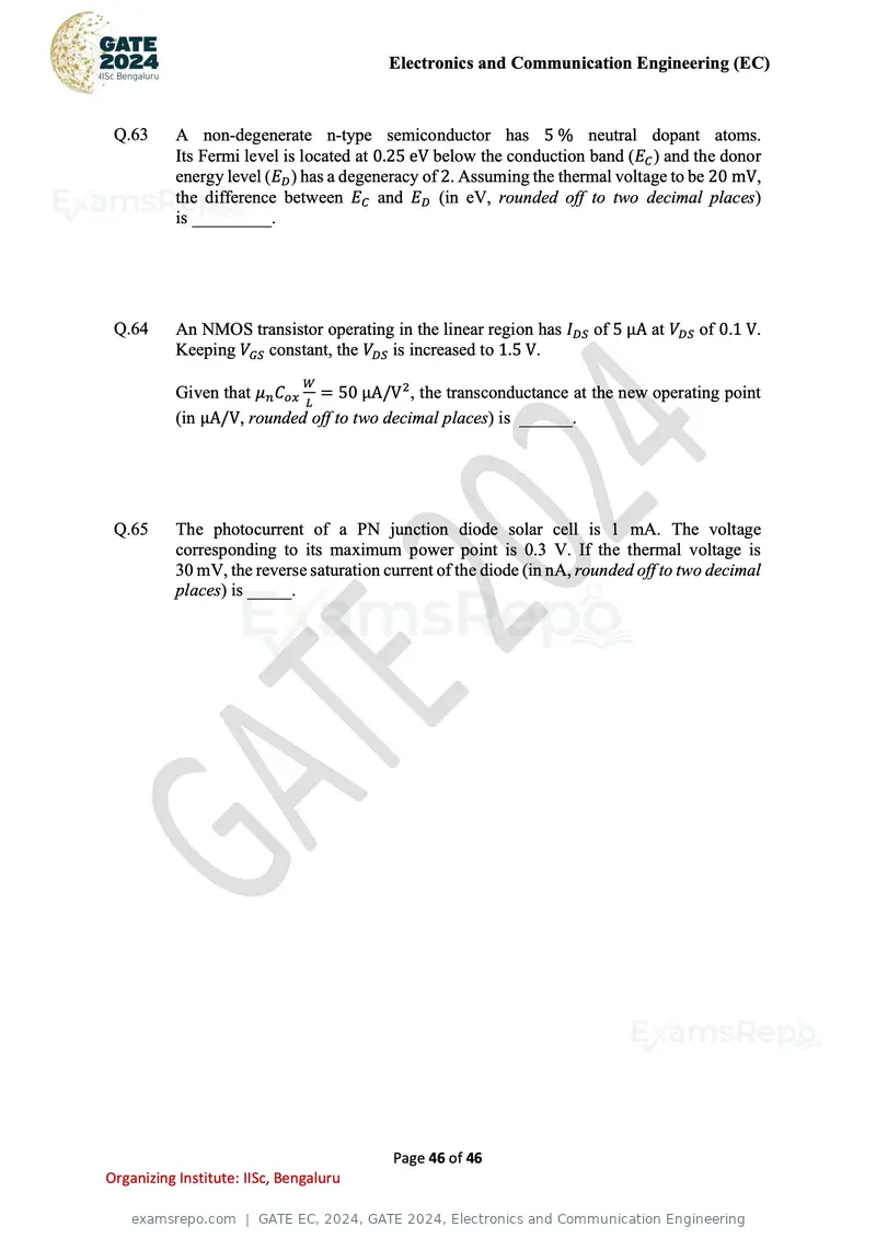
Text of page 46
Electronics and Communication Engineering (EC)


 Q.63      A non-degenerate n-type semiconductor has 5 % neutral dopant atoms.
           Its Fermi level is located at 0.25 eV below the conduction band (EC ) and the donor
           energy level (ED ) has a degeneracy of 2. Assuming the thermal voltage to be 20 mV,
           the difference between EC and ED (in eV, rounded off to two decimal places)
           is _________.


 Q.64      An NMOS transistor operating in the linear region has IDS of 5 μA at VDS of 0.1 V.
           Keeping VGS constant, the VDS is increased to 1.5 V.
                               W
           Given that μn Cox L = 50 μA/V 2 , the transconductance at the new operating point
           (in μA/V, rounded off to two decimal places) is ______.


 Q.65      The photocurrent of a PN junction diode solar cell is 1 mA. The voltage
           corresponding to its maximum power point is 0.3 V. If the thermal voltage is
           30 mV, the reverse saturation current of the diode (in nA, rounded off to two decimal
           places) is _____.


                                          Page 46 of 46
Organizing Institute: IISc, Bengaluru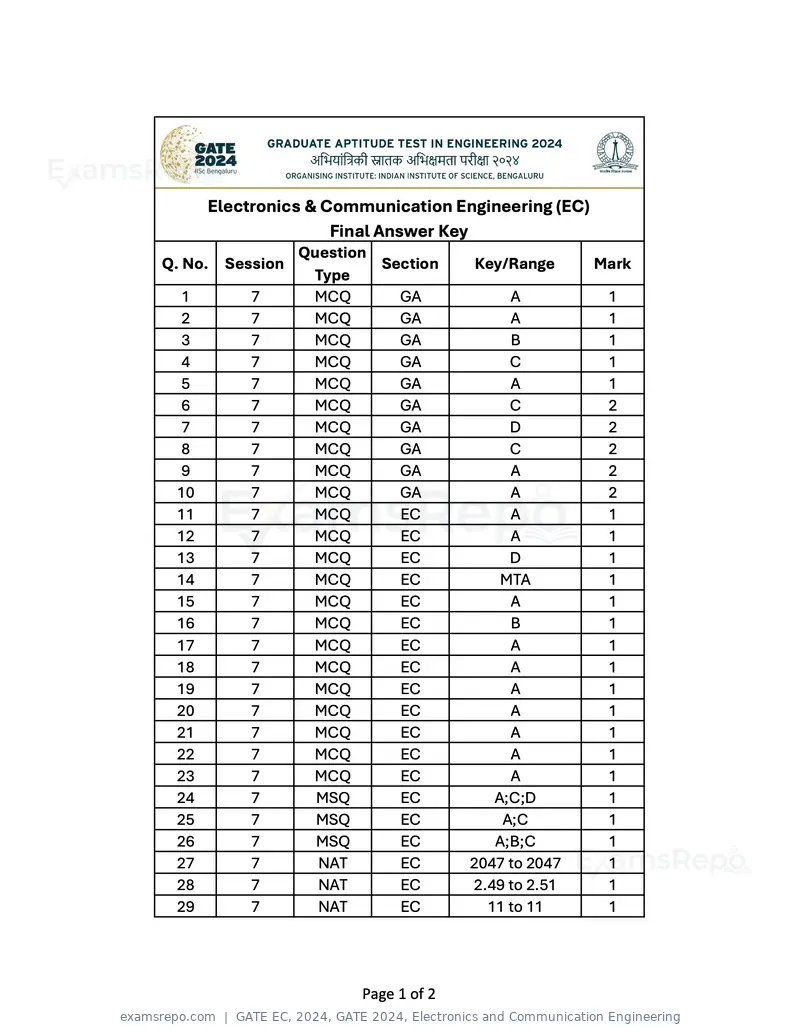
Text of page 1
Electronics & Communication Engineering (EC)
                     Final Answer Key
                   Question
Q. No.   Session            Section     Key/Range      Mark
                    Type
  1         7       MCQ       GA             A          1
  2         7       MCQ       GA             A          1
  3         7       MCQ       GA             B          1
  4         7       MCQ       GA             C          1
  5         7       MCQ       GA             A          1
  6         7       MCQ       GA             C          2
  7         7       MCQ       GA             D          2
  8         7       MCQ       GA             C          2
  9         7       MCQ       GA             A          2
 10         7       MCQ       GA             A          2
 11         7       MCQ       EC             A          1
 12         7       MCQ       EC             A          1
 13         7       MCQ       EC             D          1
 14         7       MCQ       EC            MTA         1
 15         7       MCQ       EC             A          1
 16         7       MCQ       EC             B          1
 17         7       MCQ       EC             A          1
 18         7       MCQ       EC             A          1
 19         7       MCQ       EC             A          1
 20         7       MCQ       EC             A          1
 21         7       MCQ       EC             A          1
 22         7       MCQ       EC             A          1
 23         7       MCQ       EC             A          1
 24         7        MSQ      EC           A;C;D        1
 25         7        MSQ      EC            A;C         1
 26         7        MSQ      EC           A;B;C        1
 27         7        NAT      EC        2047 to 2047    1
 28         7        NAT      EC        2.49 to 2.51    1
 29         7        NAT      EC          11 to 11      1


                          Page 1 of 2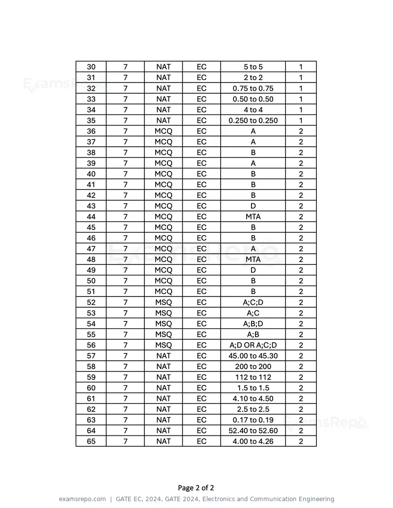
Text of page 2
30   7   NAT        EC           5 to 5       1
31   7   NAT        EC           2 to 2       1
32   7   NAT        EC        0.75 to 0.75    1
33   7   NAT        EC        0.50 to 0.50    1
34   7   NAT        EC           4 to 4       1
35   7   NAT        EC       0.250 to 0.250   1
36   7   MCQ        EC             A          2
37   7   MCQ        EC             A          2
38   7   MCQ        EC             B          2
39   7   MCQ        EC             A          2
40   7   MCQ        EC             B          2
41   7   MCQ        EC             B          2
42   7   MCQ        EC             B          2
43   7   MCQ        EC             D          2
44   7   MCQ        EC            MTA         2
45   7   MCQ        EC             B          2
46   7   MCQ        EC             B          2
47   7   MCQ        EC             A          2
48   7   MCQ        EC            MTA         2
49   7   MCQ        EC             D          2
50   7   MCQ        EC             B          2
51   7   MCQ        EC             B          2
52   7   MSQ        EC           A;C;D        2
53   7   MSQ        EC            A;C         2
54   7   MSQ        EC           A;B;D        2
55   7   MSQ        EC            A;B         2
56   7   MSQ        EC       A;D OR A;C;D     2
57   7   NAT        EC       45.00 to 45.30   2
58   7   NAT        EC         200 to 200     2
59   7   NAT        EC         112 to 112     2
60   7   NAT        EC         1.5 to 1.5     2
61   7   NAT        EC        4.10 to 4.50    2
62   7   NAT        EC         2.5 to 2.5     2
63   7   NAT        EC        0.17 to 0.19    2
64   7   NAT        EC       52.40 to 52.60   2
65   7   NAT        EC        4.00 to 4.26    2


               Page 2 of 2
Page 1 of 46
Source: GATE. Question paper published by GATE.