
GATE EC 2026: Electronics and Communication Engineering

Text of page 1
Electronics & Communication Engineering (EC)


General Aptitude (GA)
Q.1 – Q.5 Carry ONE mark Each

 Q.1         Among the following options, the antonym of the word ‘nocturnal’ is _________.


 (A)         normal


 (B)         diurnal


 (C)         abnormal


 (D)         exceptional


Organizing Institute: IIT Guwahati         Page 1 of 58
Text of page 2
Electronics & Communication Engineering (EC)


 Q.2         The statements (S1), (S2), and (S3) pertain to the scores obtained by students in
             an exam. The maximum possible marks in the exam is 150.

             (S1) The highest score is 100.

             (S2) The fourth highest score is 76.

             (S3) There are at least four students whose scores are within 25 of each other.

             Which one of the following options is necessarily correct?


 (A)         (S1) and (S2) together imply (S3)


 (B)         (S1) and (S3) together imply (S2)


 (C)         (S2) and (S3) together imply (S1)


 (D)         (S1) implies (S3)


Organizing Institute: IIT Guwahati            Page 2 of 58
Text of page 3
Electronics & Communication Engineering (EC)


 Q.3         The figure below has exactly three intersecting line segments with a rectangular
             portion WXYZ missing. Which one of the following options P, Q, R, and S is the
             missing portion WXYZ?


                                     P                                   Q


                                     R                                   S


             P
 (A)

             Q
 (B)


 (C)         R


 (D)         S


Organizing Institute: IIT Guwahati          Page 3 of 58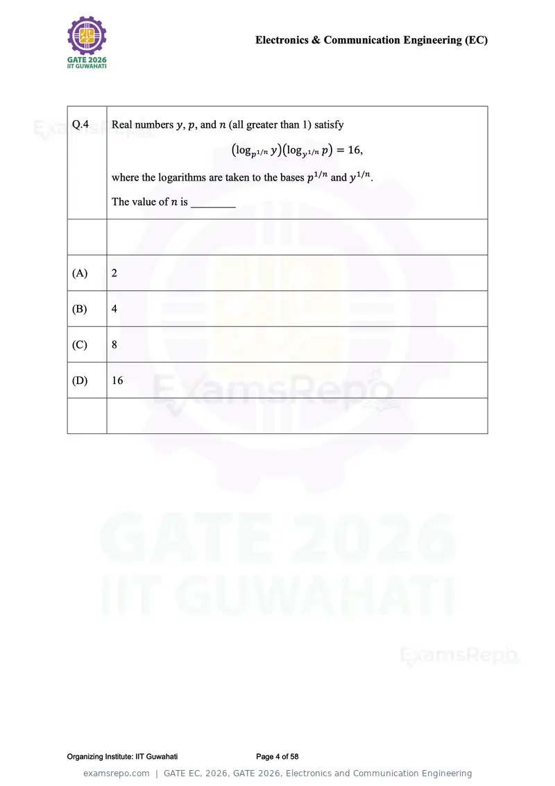
Text of page 4
Electronics & Communication Engineering (EC)


 Q.4         Real numbers y, p, and n (all greater than 1) satisfy

                                        (log p1/n y)(log y 1/n p) = 16,

             where the logarithms are taken to the bases p1/n and y1/n .

             The value of n is ________


 (A)         2


 (B)         4


 (C)         8


 (D)         16


Organizing Institute: IIT Guwahati            Page 4 of 58
Text of page 5
Electronics & Communication Engineering (EC)


 Q.5       The following observation is made about the scores obtained by 100 students in an
           exam:

           ‘For each student, there exists another student in the class such that their scores are
           at most ten marks away.’

           If the above statement is false, which one of the following statements is necessarily
           true?


 (A)       For each student, the scores of all the other students are more than 10 marks away.


 (B)       There exists at least one student in the class for whom the scores of all the other
           students are more than 10 marks away.


 (C)       There is exactly one student in the class for whom the scores of some students are
           more than 10 marks away.


 (D)       For each student, the score of exactly one other student is more than 10 marks
           away.


Organizing Institute: IIT Guwahati            Page 5 of 58
Text of page 6
Electronics & Communication Engineering (EC)


Q.6 – Q.10 Carry TWO marks Each

 Q.6         Each one of the following clues contains a keyword that is partially filled.

             Clue 1: Synonym of recognize (8 letters): _ D _ NT_ FY

             Clue 2: A story long enough to fill a book (5 letters): _ _ _ EL

             Clue 3: Two of something (6 letters): _ _ _ PLE

             Clue 4: A fraction of something, split equally into two parts (4 letters): _ _ _ F

             The first letter of each of the keywords can be rearranged to form a four-letter
             word.

             Which one of the options below is a possible choice for the four-letter word?


 (A)         CHIN


 (B)         COIN


 (C)         ITCH


 (D)         NOSE


Organizing Institute: IIT Guwahati            Page 6 of 58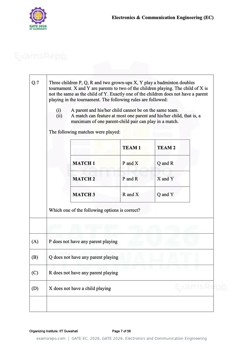
Text of page 7
Electronics & Communication Engineering (EC)


 Q.7         Three children P, Q, R and two grown-ups X, Y play a badminton doubles
             tournament. X and Y are parents to two of the children playing. The child of X is
             not the same as the child of Y. Exactly one of the children does not have a parent
             playing in the tournament. The following rules are followed:

                  (i)        A parent and his/her child cannot be on the same team.
                  (ii)       A match can feature at most one parent and his/her child, that is, a
                             maximum of one parent-child pair can play in a match.

             The following matches were played:


                                                        TEAM 1            TEAM 2


                              MATCH 1                   P and X           Q and R


                              MATCH 2                   P and R           X and Y


                              MATCH 3                   R and X           Q and Y


             Which one of the following options is correct?


 (A)         P does not have any parent playing


 (B)         Q does not have any parent playing


 (C)         R does not have any parent playing


 (D)         X does not have a child playing


Organizing Institute: IIT Guwahati                Page 7 of 58
Text of page 8
Electronics & Communication Engineering (EC)


 Q.8         Let Pk represent the perimeter of a square with sides of length k. The value of the
             expression P1 + P2 + P3 + ⋯ + P10 is __________


 (A)         55


 (B)         110


 (C)         220


 (D)         440


Organizing Institute: IIT Guwahati           Page 8 of 58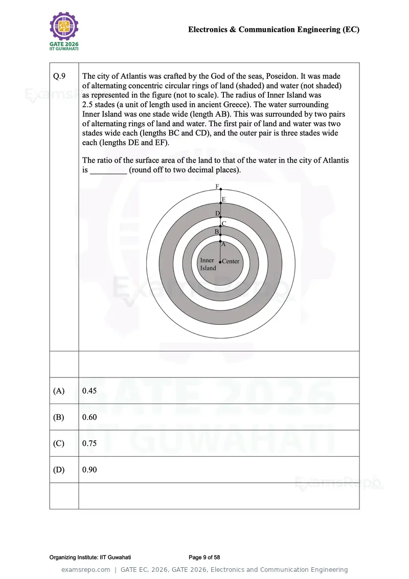
Text of page 9
Electronics & Communication Engineering (EC)


 Q.9         The city of Atlantis was crafted by the God of the seas, Poseidon. It was made
             of alternating concentric circular rings of land (shaded) and water (not shaded)
             as represented in the figure (not to scale). The radius of Inner Island was
             2.5 stades (a unit of length used in ancient Greece). The water surrounding
             Inner Island was one stade wide (length AB). This was surrounded by two pairs
             of alternating rings of land and water. The first pair of land and water was two
             stades wide each (lengths BC and CD), and the outer pair is three stades wide
             each (lengths DE and EF).

             The ratio of the surface area of the land to that of the water in the city of Atlantis
             is _________ (round off to two decimal places).


 (A)         0.45


 (B)         0.60


 (C)         0.75


 (D)         0.90


Organizing Institute: IIT Guwahati             Page 9 of 58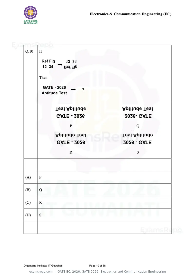
Text of page 10
Electronics & Communication Engineering (EC)


 Q.10        If


             Then


                                     P                            Q


                                     R                            S


 (A)         P


 (B)         Q


 (C)         R


 (D)         S


Organizing Institute: IIT Guwahati       Page 10 of 58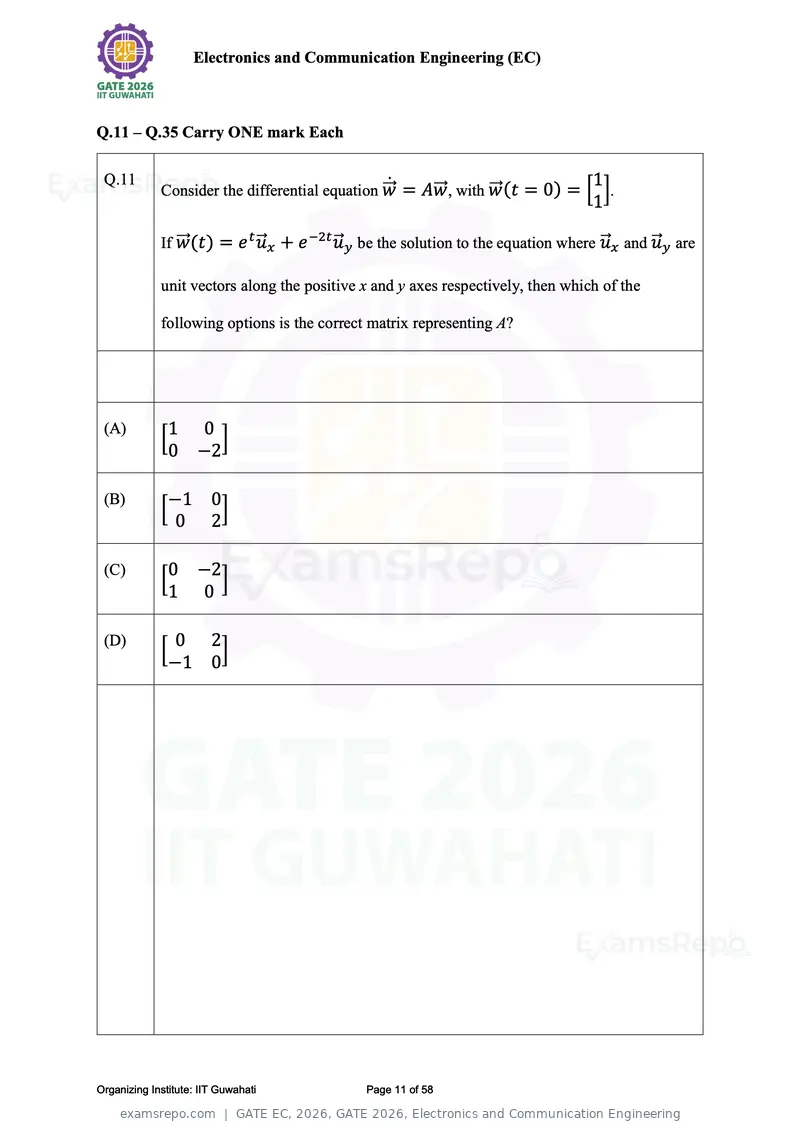
Text of page 11
Electronics and Communication Engineering (EC)


Q.11 – Q.35 Carry ONE mark Each

 Q.11                                                                            1
                                                ẇ = Aw
             Consider the differential equation ⃗⃗    ⃗⃗ , with ⃗⃗w(t = 0) = [ ].
                                                                                 1

                w(t) = e t ⃗ux + e −2t ⃗uy be the solution to the equation where ⃗ux and ⃗uy are
             If ⃗⃗

             unit vectors along the positive x and y axes respectively, then which of the

             following options is the correct matrix representing A?


 (A)             1 0
             [        ]
                 0 −2

 (B)             −1 0
             [        ]
                 0 2

 (C)             0 −2
             [        ]
                 1 0

 (D)             0 2
             [        ]
                 −1 0


Organizing Institute: IIT Guwahati           Page 11 of 58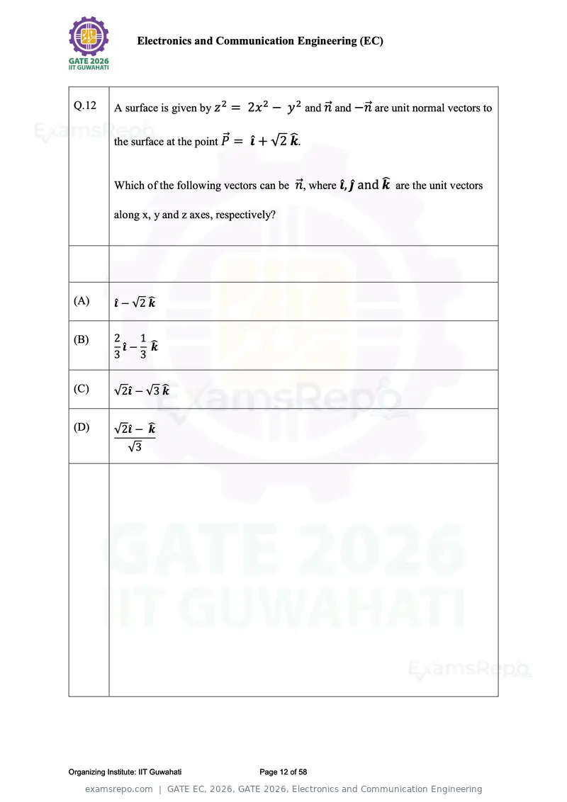
Text of page 12
Electronics and Communication Engineering (EC)


 Q.12        A surface is given by z 2 = 2x 2 − y 2 and ⃗n and −n
                                                                ⃗ are unit normal vectors to

                                                  ̂.
                                      ⃗ = î + √2 k
             the surface at the point P


                                                                        ̂ are the unit vectors
             Which of the following vectors can be ⃗n, where î, ĵ and k

             along x, y and z axes, respectively?


 (A)                 ̂
             î − √2 k


 (B)         2     1
               î − ̂k
             3     3

 (C)                   ̂
             √2î − √3 k


 (D)                ̂
             √2î − k
                 √3


Organizing Institute: IIT Guwahati           Page 12 of 58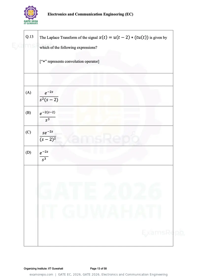
Text of page 13
Electronics and Communication Engineering (EC)


 Q.13        The Laplace Transform of the signal x(t) = u(t − 2) ∗ (tu(t)) is given by

             which of the following expressions?


             [“∗” represents convolution operator]


 (A)             e −2s
             s 2 (s − 2)

 (B)         e −2(s−2)
                s3

 (C)          se −2s
             (s − 2)2

 (D)         e −2s
              s3


Organizing Institute: IIT Guwahati          Page 13 of 58
Text of page 14
Electronics and Communication Engineering (EC)


 Q.14        Consider carrier transport in a Zener diode in the breakdown region.


             Which is the dominant transport mechanism for current flow in this case?


 (A)           Drift


 (B)           Diffusion


 (C)           Tunneling


 (D)           Ballistic transport


Organizing Institute: IIT Guwahati          Page 14 of 58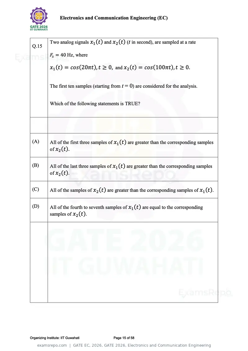
Text of page 15
Electronics and Communication Engineering (EC)


             Two analog signals x1 (t) and x2 (t) (t in second), are sampled at a rate
 Q.15
             Fs = 40 Hz, where

             x1 (t) = cos(20πt), t ≥ 0, and x2 (t) = cos(100πt), t ≥ 0.


             The first ten samples (starting from t = 0) are considered for the analysis.


             Which of the following statements is TRUE?


 (A)         All of the first three samples of x1 (t) are greater than the corresponding samples
             of x2 (t).


 (B)         All of the last three samples of x1 (t) are greater than the corresponding samples
             of x2 (t).


 (C)         All of the samples of x2 (t) are greater than the corresponding samples of x1 (t).


 (D)         All of the fourth to seventh samples of x1 (t) are equal to the corresponding
             samples of x2 (t).


Organizing Institute: IIT Guwahati           Page 15 of 58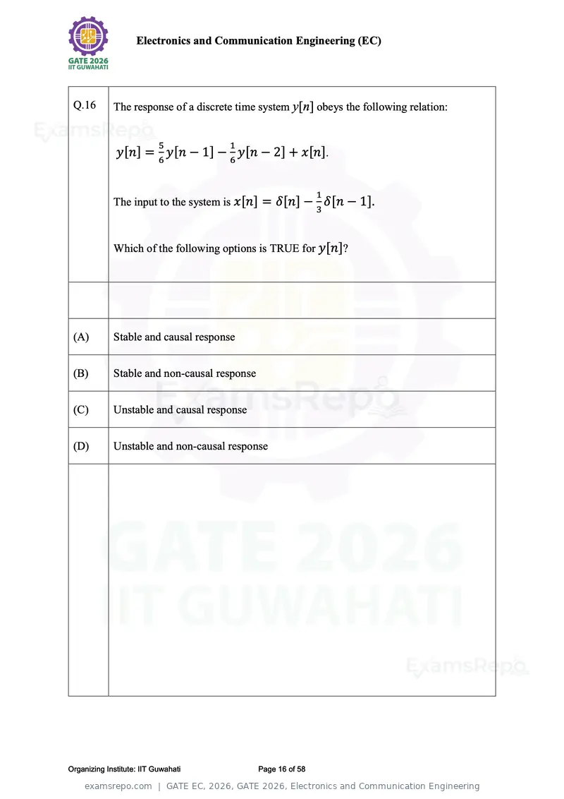
Text of page 16
Electronics and Communication Engineering (EC)


 Q.16        The response of a discrete time system y[n] obeys the following relation:


                           5          1
              y[n] = y[n − 1] − y[n − 2] + x[n].
                           6          6


                                                              1
             The input to the system is x[n] = δ[n] − δ[n − 1].
                                                              3


             Which of the following options is TRUE for y[n]?


 (A)         Stable and causal response


 (B)         Stable and non-causal response


 (C)         Unstable and causal response


 (D)         Unstable and non-causal response


Organizing Institute: IIT Guwahati            Page 16 of 58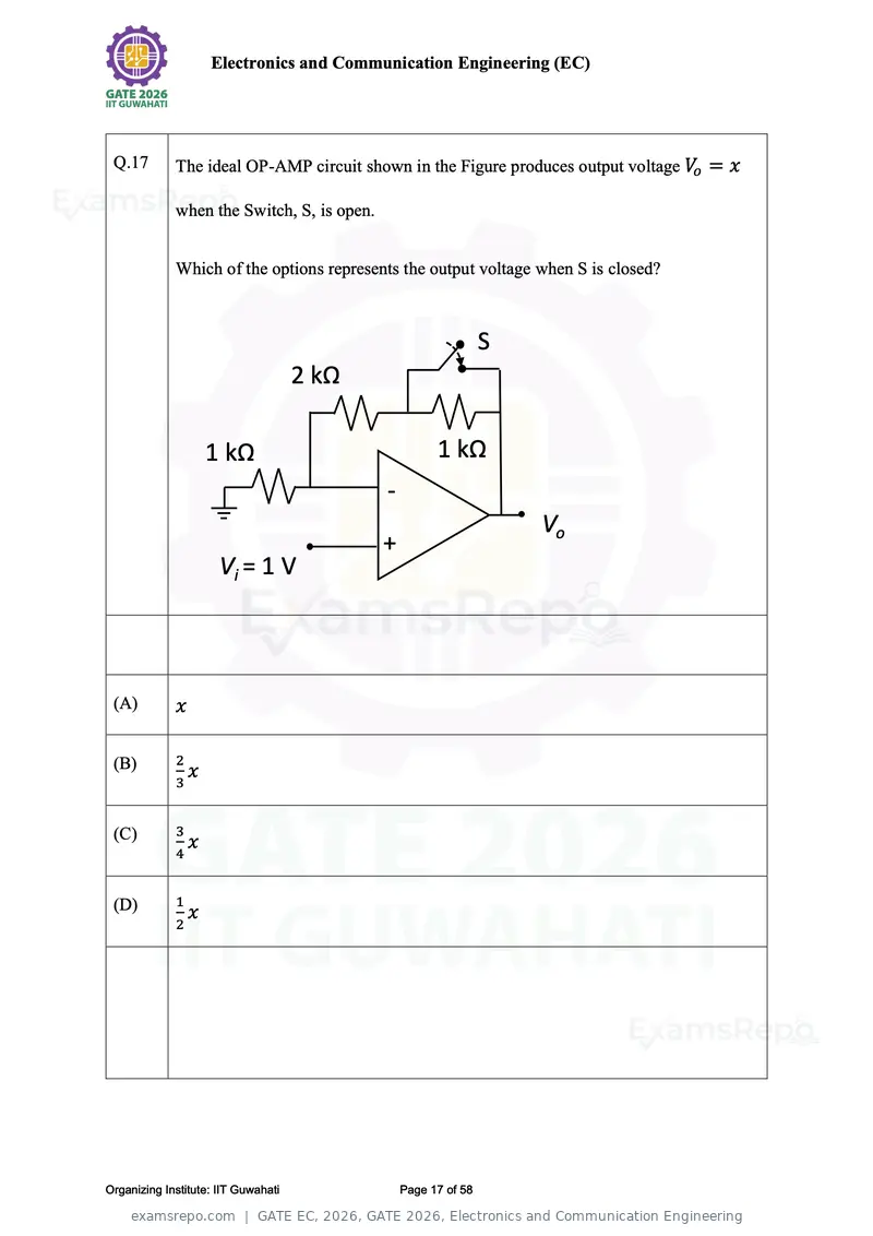
Text of page 17
Electronics and Communication Engineering (EC)


 Q.17        The ideal OP-AMP circuit shown in the Figure produces output voltage Vo = x

             when the Switch, S, is open.


             Which of the options represents the output voltage when S is closed?


                                                                S
                                     2 kΩ

                     1 kΩ                             1 kΩ
                                            -
                                                                    Vo
                                            +
                      Vi = 1 V


 (A)         x

 (B)         2
                 x
             3


 (C)         3
                 x
             4


 (D)         1
                 x
             2


Organizing Institute: IIT Guwahati              Page 17 of 58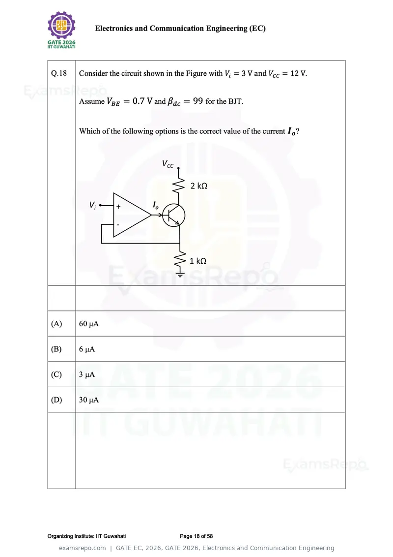
Text of page 18
Electronics and Communication Engineering (EC)


 Q.18        Consider the circuit shown in the Figure with Vi = 3 V and VCC = 12 V.


             Assume VBE = 0.7 V and βdc = 99 for the BJT.


             Which of the following options is the correct value of the current Io ?


 (A)         60 μA


 (B)         6 μA


 (C)         3 μA


 (D)         30 μA


Organizing Institute: IIT Guwahati           Page 18 of 58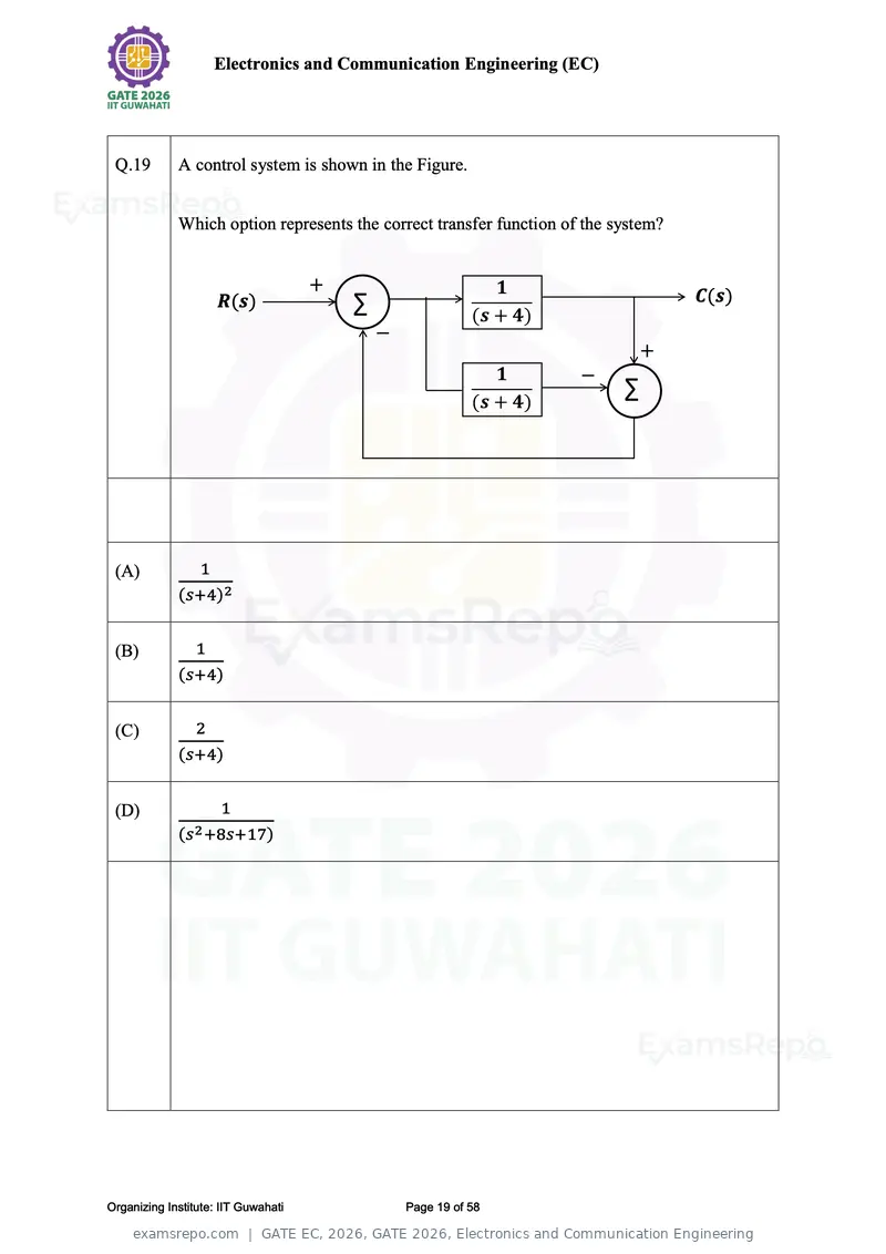
Text of page 19
Electronics and Communication Engineering (EC)


 Q.19        A control system is shown in the Figure.


             Which option represents the correct transfer function of the system?


                                     +
                       ( )               ∑                                          ( )
                                             −
                                                                               +
                                                                     −
                                                                           ∑


 (A)            1
             (s+4)2


 (B)           1
             (s+4)


 (C)           2
             (s+4)


 (D)                 1
             (s2 +8s+17)


Organizing Institute: IIT Guwahati               Page 19 of 58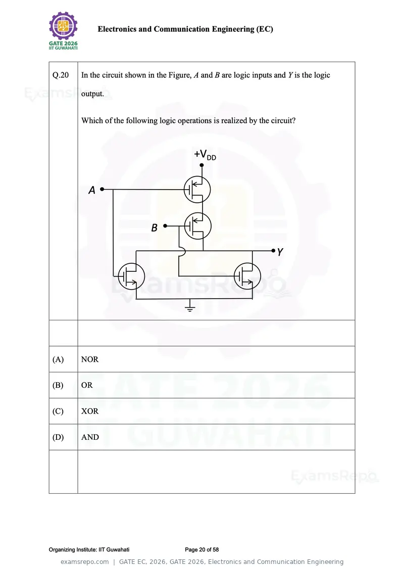
Text of page 20
Electronics and Communication Engineering (EC)


 Q.20        In the circuit shown in the Figure, A and B are logic inputs and Y is the logic

             output.


             Which of the following logic operations is realized by the circuit?


                                                +VDD


                A


                                     B

                                                                           Y


 (A)         NOR


 (B)         OR


 (C)         XOR


 (D)         AND


Organizing Institute: IIT Guwahati           Page 20 of 58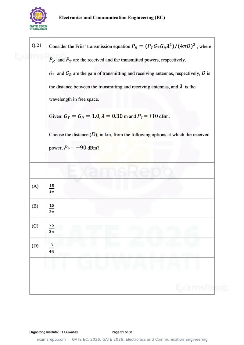
Text of page 21
Electronics and Communication Engineering (EC)


 Q.21        Consider the Friis’ transmission equation PR = (PT GT GR λ2 )⁄(4πD)2 , where

             PR and PT are the received and the transmitted powers, respectively.

             GT and GR are the gain of transmitting and receiving antennas, respectively, D is

             the distance between the transmitting and receiving antennas, and λ is the

             wavelength in free space.


             Given: GT = GR = 1.0, λ = 0.30 m and PT = +10 dBm.


             Choose the distance (D), in km, from the following options at which the received

             power, PR = −90 dBm?


 (A)         15
             4π


 (B)         15
             2π


 (C)         75
             2π


 (D)          3
             4π


Organizing Institute: IIT Guwahati          Page 21 of 58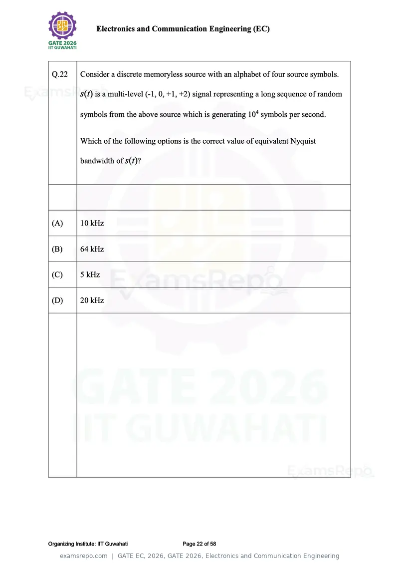
Text of page 22
Electronics and Communication Engineering (EC)


 Q.22        Consider a discrete memoryless source with an alphabet of four source symbols.

             s(t) is a multi-level (-1, 0, +1, +2) signal representing a long sequence of random

             symbols from the above source which is generating 104 symbols per second.


             Which of the following options is the correct value of equivalent Nyquist

             bandwidth of s(t)?


 (A)         10 kHz


 (B)         64 kHz


 (C)         5 kHz


 (D)         20 kHz


Organizing Institute: IIT Guwahati           Page 22 of 58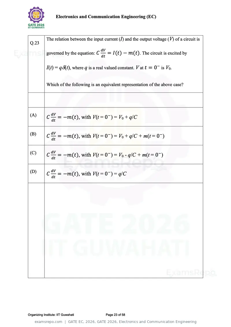
Text of page 23
Electronics and Communication Engineering (EC)
The relation between the input current (I) and the output voltage (V) of a circuit is
Q.23
dV
governed by the equation: C = I(t) − m(t). The circuit is excited by
dt
I(t) = q(t), where q is a real valued constant. V at t = 0− is V0.
Which of the following is an equivalent representation of the above case?
(A) dV
C = −m(t), with V(t = 0− ) = V0 + q/C
dt
(B) dV
C = −m(t), with V(t = 0− ) = V0 + q/C + m(t = 0− )
dt
(C) dV
C = −m(t), with V(t = 0− ) = V0 - q/C + m(t = 0− )
dt
(D) dV
C = −m(t), with V(t = 0− ) = q/C
dt
Organizing Institute: IIT Guwahati Page 23 of 58
Text of page 24
Electronics and Communication Engineering (EC)


             The electric field of a monochromatic plane wave travelling in a lossless isotropic
 Q.24
             and homogenous medium is given by

             E⃗ (z, t) = E0 [x̂cos(ωt − kz) + ŷsin(ωt − kz)]

             in a right-handed orthogonal co-ordinate system.


             Which of the following is the correct polarization of the electromagnetic wave?


 (A)         Right-handed circularly polarized


 (B)         Left-handed circularly polarized


 (C)         Linearly polarized


 (D)         Linearly polarized with −45o angle to x̂


Organizing Institute: IIT Guwahati           Page 24 of 58
Text of page 25
Electronics and Communication Engineering (EC)


 Q.25        Consider a p-n junction diode when it is forward biased with 2 V.


             Which of the following is/are the correct magnitude(s) of the energy difference

             between quasi Fermi-levels, Efn in the n-side and Efp in the p-side?


 (A)           2 eV


 (B)           1 eV


 (C)           2V


 (D)           1V


Organizing Institute: IIT Guwahati           Page 25 of 58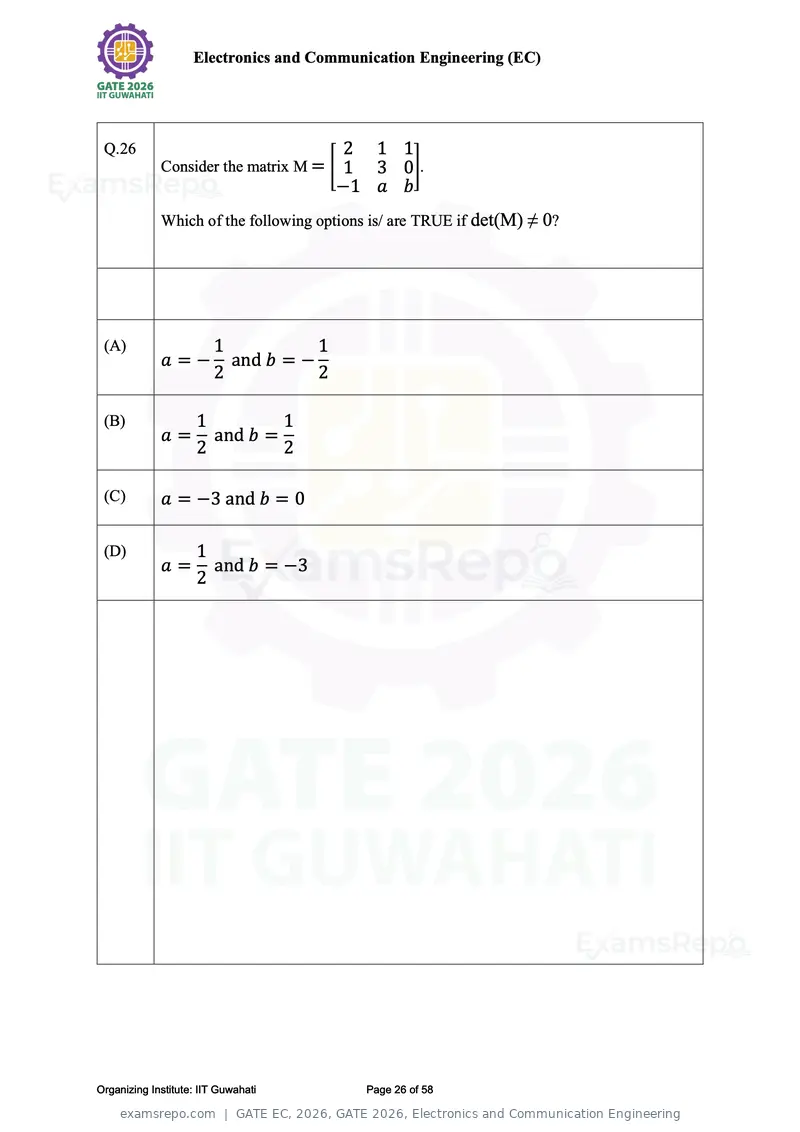
Text of page 26
Electronics and Communication Engineering (EC)


 Q.26                                   2  1 1
             Consider the matrix M = [ 1   3 0].
                                        −1 a b
             Which of the following options is/ are TRUE if det(M) ≠ 0?


 (A)                    1           1
             a=−          and b = −
                        2           2

 (B)                 1         1
             a=        and b =
                     2         2

 (C)         a = −3 and b = 0

 (D)                 1
             a=        and b = −3
                     2


Organizing Institute: IIT Guwahati          Page 26 of 58
Text of page 27
Electronics and Communication Engineering (EC)


 Q.27        A binary ripple counter is designed to count (0)10 to (64)10.


             Which of the following is/are the number of flip-flops required to design the

             counter?


 (A)         6


 (B)         7


 (C)         4


 (D)         5


Organizing Institute: IIT Guwahati           Page 27 of 58
Text of page 28
Electronics and Communication Engineering (EC)


 Q.28        Which option(s) represents/ represent the dielectric loss tangent of a substrate?


 (A)         Ratio of the real to imaginary parts of the total displacement current


 (B)         (ωε ′′ + σ)⁄(ωε′)

 (C)         Ratio of the electric susceptibility to permittivity


 (D)         Ratio of the polarization vector ⃗
                                              P to the displacement vector ⃗D


Organizing Institute: IIT Guwahati            Page 28 of 58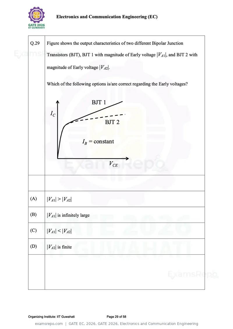
Text of page 29
Electronics and Communication Engineering (EC)


 Q.29        Figure shows the output characteristics of two different Bipolar Junction

             Transistors (BJT), BJT 1 with magnitude of Early voltage |VA1|, and BJT 2 with

             magnitude of Early voltage |VA2|.


             Which of the following options is/are correct regarding the Early voltages?


                                         BJT 1
                IC
                                              BJT 2


                                     IB = constant


                                                  VCE


 (A)         |VA1| > |VA2|

 (B)         |VA1| is infinitely large

 (C)         |VA1| < |VA2|

 (D)         |VA2| is finite


Organizing Institute: IIT Guwahati               Page 29 of 58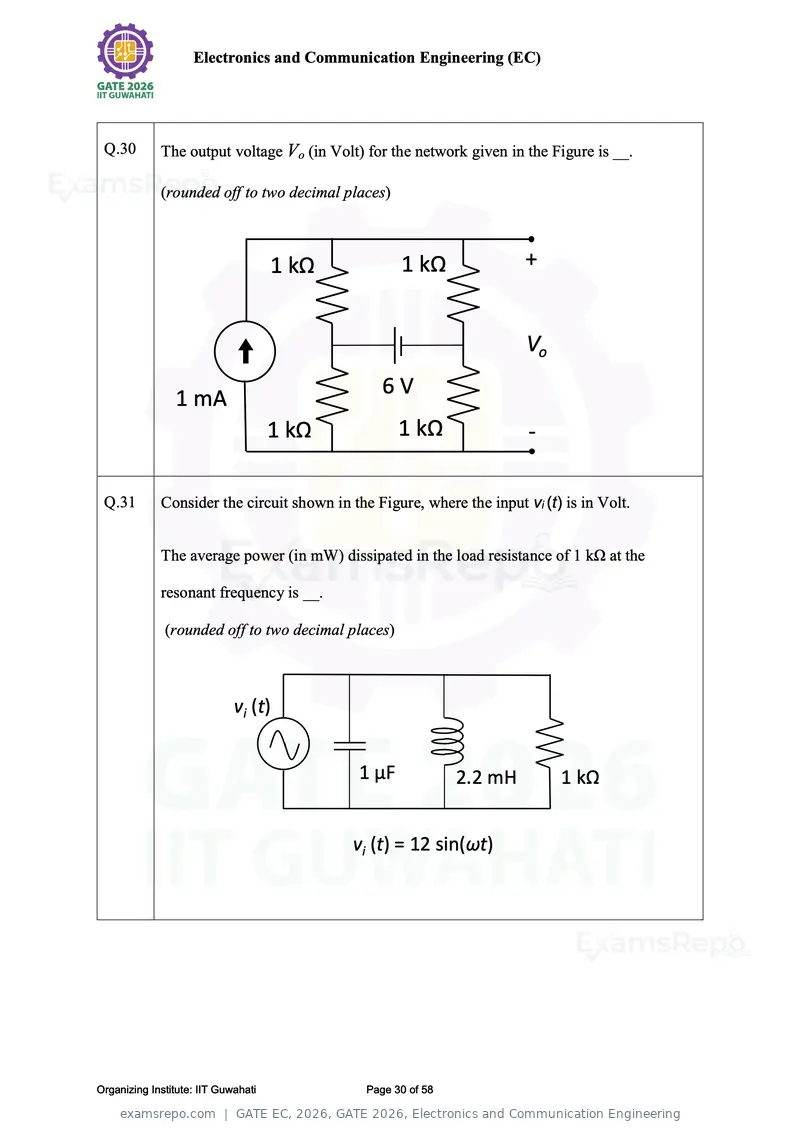
Text of page 30
Electronics and Communication Engineering (EC)


 Q.30        The output voltage Vo (in Volt) for the network given in the Figure is __.

             (rounded off to two decimal places)


                                     1 kΩ           1 kΩ                +


                                                                        Vo
                                                 6V
                1 mA
                                     1 kΩ           1 kΩ                -

 Q.31        Consider the circuit shown in the Figure, where the input vi (t) is in Volt.


             The average power (in mW) dissipated in the load resistance of 1 kΩ at the

             resonant frequency is __.

              (rounded off to two decimal places)


                             vi (t)


                                             1 μF             2.2 mH         1 kΩ


                                            vi (t) = 12 sin(ωt)


Organizing Institute: IIT Guwahati            Page 30 of 58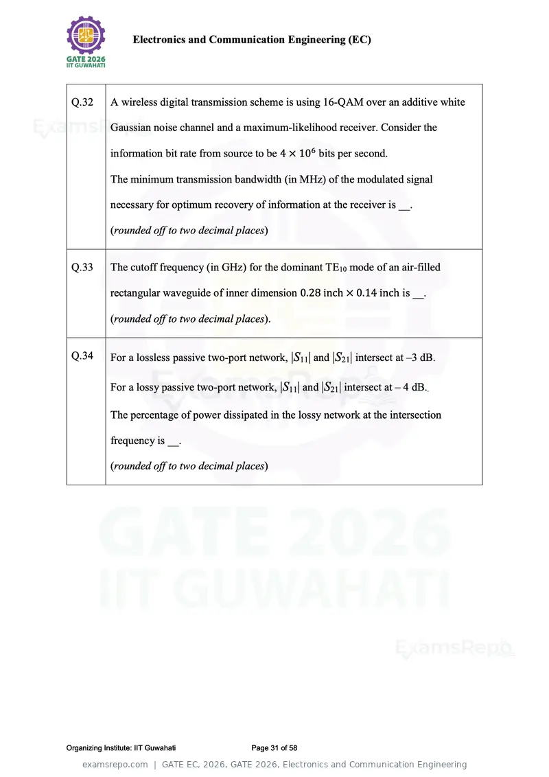
Text of page 31
Electronics and Communication Engineering (EC)


 Q.32        A wireless digital transmission scheme is using 16-QAM over an additive white

             Gaussian noise channel and a maximum-likelihood receiver. Consider the

             information bit rate from source to be 4 × 106 bits per second.

             The minimum transmission bandwidth (in MHz) of the modulated signal

             necessary for optimum recovery of information at the receiver is __.

             (rounded off to two decimal places)


 Q.33        The cutoff frequency (in GHz) for the dominant TE10 mode of an air-filled

             rectangular waveguide of inner dimension 0.28 inch × 0.14 inch is __.

             (rounded off to two decimal places).


 Q.34        For a lossless passive two-port network, |S11| and |S21| intersect at –3 dB.

             For a lossy passive two-port network, |S11| and |S21| intersect at – 4 dB..

             The percentage of power dissipated in the lossy network at the intersection

             frequency is __.

             (rounded off to two decimal places)


Organizing Institute: IIT Guwahati            Page 31 of 58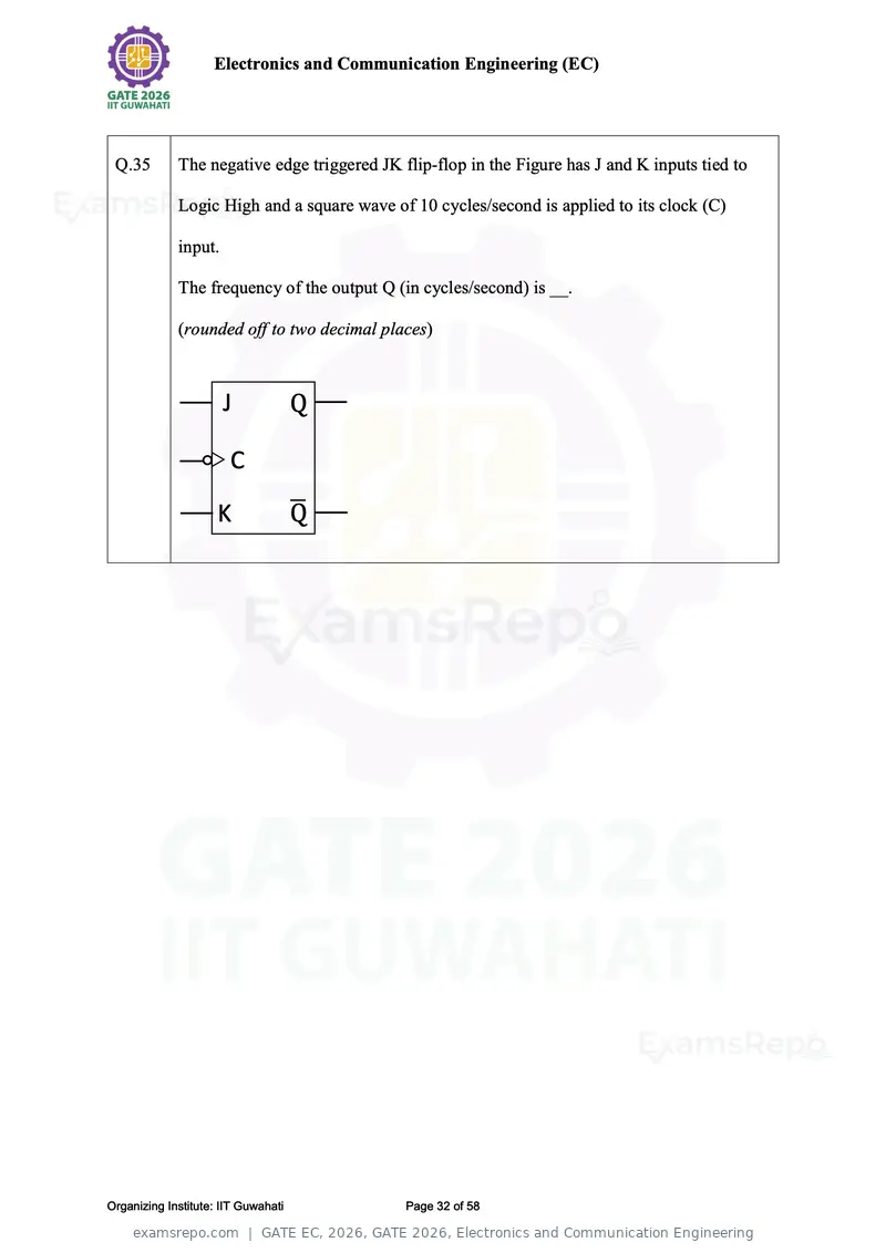
Text of page 32
Electronics and Communication Engineering (EC)


 Q.35        The negative edge triggered JK flip-flop in the Figure has J and K inputs tied to

             Logic High and a square wave of 10 cycles/second is applied to its clock (C)

             input.

             The frequency of the output Q (in cycles/second) is __.

             (rounded off to two decimal places)


                       C
                     K


Organizing Institute: IIT Guwahati           Page 32 of 58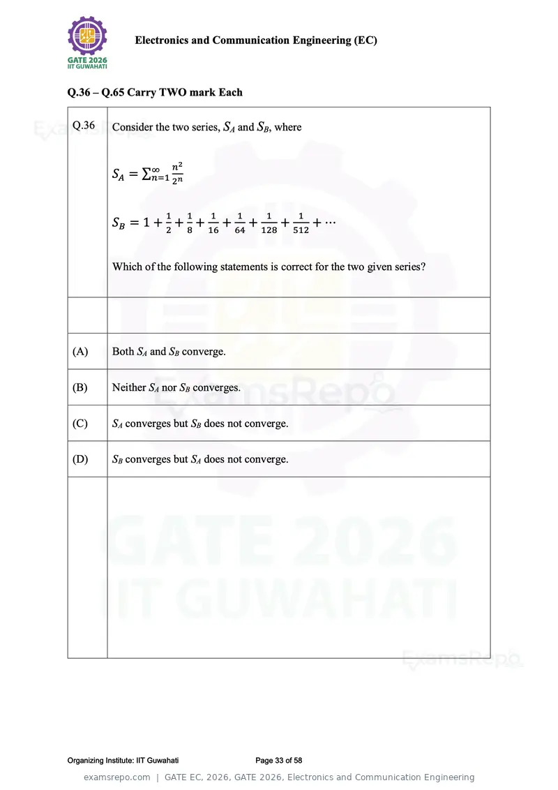
Text of page 33
Electronics and Communication Engineering (EC)


Q.36 – Q.65 Carry TWO mark Each

 Q.36        Consider the two series, SA and SB, where


                                  n2
             SA = ∑∞
                   n=1 n          2


                              1        1   1        1        1         1
             SB = 1 + + +                       +        +         +         +⋯
                              2        8   16       64       128       512


             Which of the following statements is correct for the two given series?


 (A)         Both SA and SB converge.


 (B)         Neither SA nor SB converges.


 (C)         SA converges but SB does not converge.


 (D)         SB converges but SA does not converge.


Organizing Institute: IIT Guwahati                       Page 33 of 58
Text of page 34
Electronics and Communication Engineering (EC)


 Q.37        The continuous time signal x(t) is real, periodic with period T and satisfies the

             Dirichlet conditions.

                                                                           2πnt
                                                                      j(        )
             The Fourier series representation of x(t) = ∑∞
                                                          −∞ an e           T     and   x(t) satisfies

                                     T
             the following: x (t − ) = −x(t).
                                     2


             For any integer m, which of the following options is correct?


 (A)         a2m = 0

 (B)         a2m = 1

 (C)         a2m = a2m+1

 (D)         a2m = -1


Organizing Institute: IIT Guwahati           Page 34 of 58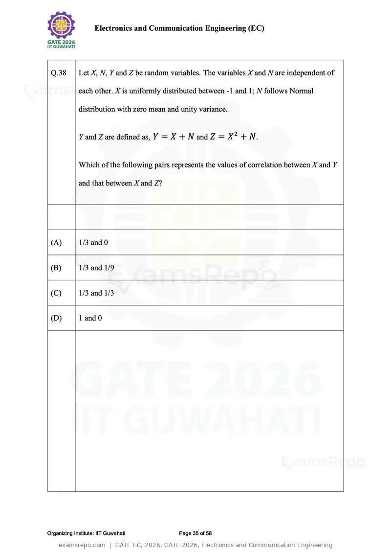
Text of page 35
Electronics and Communication Engineering (EC)


 Q.38        Let X, N, Y and Z be random variables. The variables X and N are independent of

             each other. X is uniformly distributed between -1 and 1; N follows Normal

             distribution with zero mean and unity variance.


             Y and Z are defined as, Y = X + N and Z = X 2 + N.


             Which of the following pairs represents the values of correlation between X and Y

             and that between X and Z?


 (A)         1/3 and 0


 (B)         1/3 and 1/9


 (C)         1/3 and 1/3


 (D)         1 and 0


Organizing Institute: IIT Guwahati          Page 35 of 58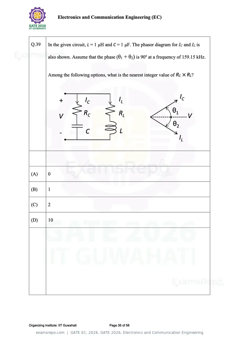
Text of page 36
Electronics and Communication Engineering (EC)


 Q.39        In the given circuit, L = 1 μH and C = 1 μF. The phasor diagram for IC and IL is

             also shown. Assume that the phase (θ1 + θ2) is 90o at a frequency of 159.15 kHz.


             Among the following options, what is the nearest integer value of RC × RL?


                                     IC            IL                              IC
                     +
                                     RC           RL                          θ1
                     V                                                                  V
                                                                              θ2
                     -               C             L
                                                                                   IL


 (A)         0


 (B)         1


 (C)         2


 (D)         10


Organizing Institute: IIT Guwahati           Page 36 of 58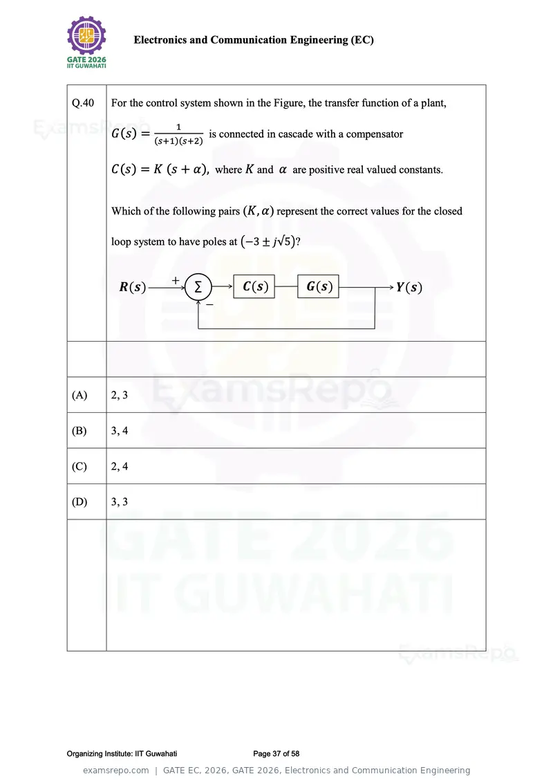
Text of page 37
Electronics and Communication Engineering (EC)


 Q.40        For the control system shown in the Figure, the transfer function of a plant,

                                 1
             G(s) = (s+1)(s+2) is connected in cascade with a compensator

             C(s) = K (s + α), where K and α are positive real valued constants.


             Which of the following pairs (K, α) represent the correct values for the closed

             loop system to have poles at (−3 ± j√5)?


                                     ∑


 (A)         2, 3


 (B)         3, 4


 (C)         2, 4


 (D)         3, 3


Organizing Institute: IIT Guwahati           Page 37 of 58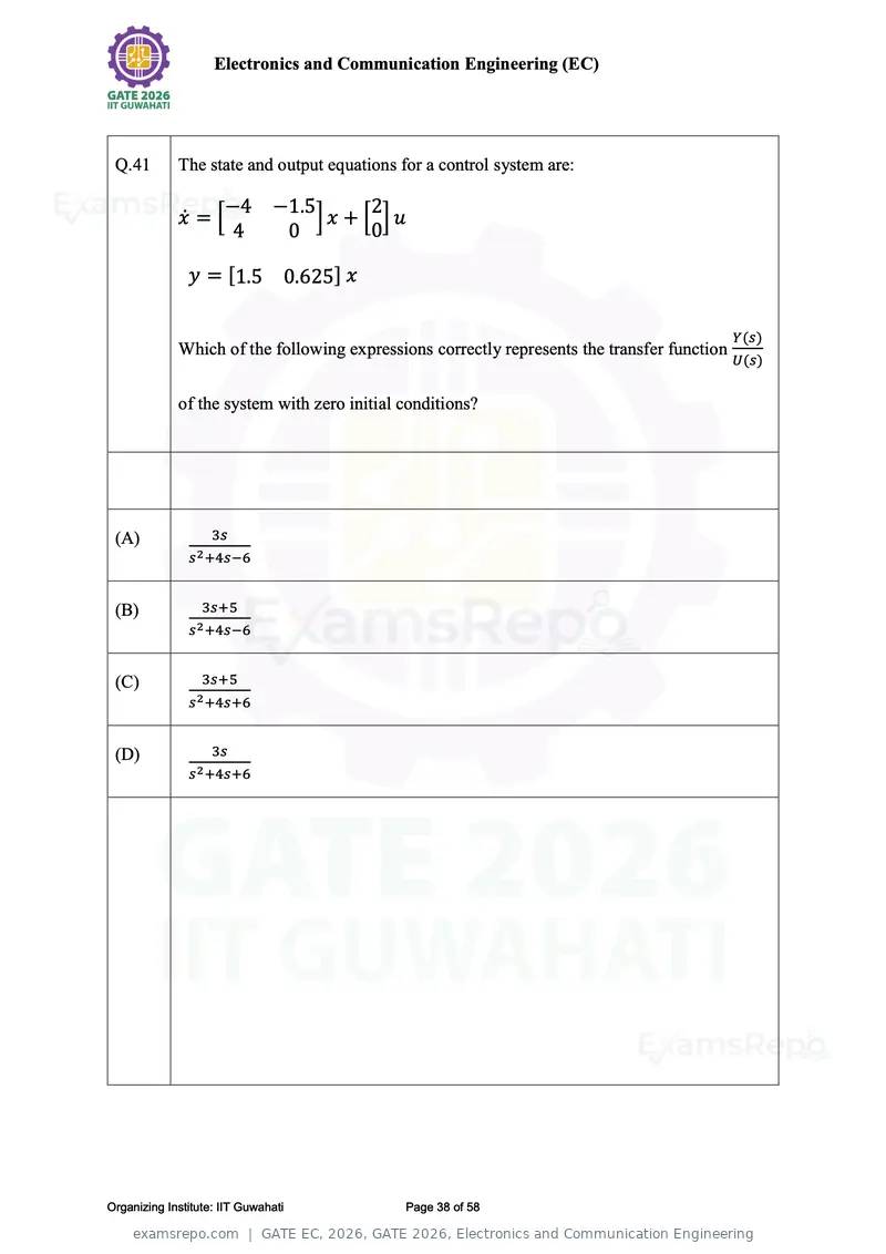
Text of page 38
Electronics and Communication Engineering (EC)


 Q.41        The state and output equations for a control system are:

                   −4          −1.5       2
             ẋ = [                 ]x + [ ]u
                    4           0         0

               y = [1.5 0.625] x

                                                                                             Y(s)
             Which of the following expressions correctly represents the transfer function
                                                                                             U(s)

             of the system with zero initial conditions?


 (A)                3s
               s 2 +4s−6


 (B)              3s+5
               s 2 +4s−6


 (C)              3s+5
               s 2 +4s+6


 (D)                3s
               s 2 +4s+6


Organizing Institute: IIT Guwahati              Page 38 of 58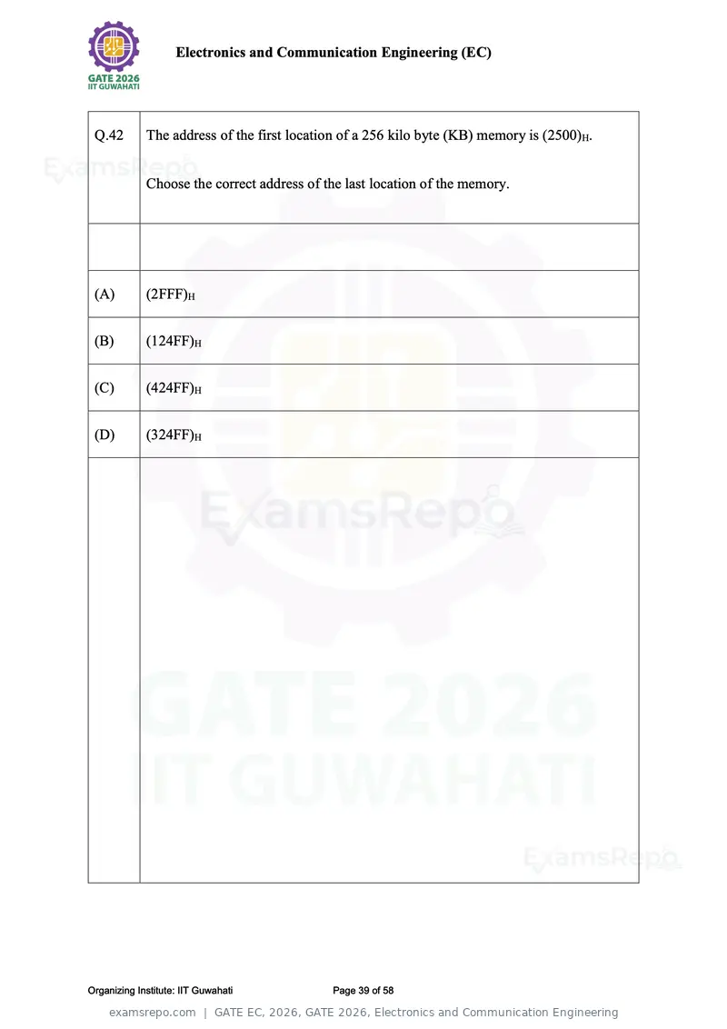
Text of page 39
Electronics and Communication Engineering (EC)


 Q.42        The address of the first location of a 256 kilo byte (KB) memory is (2500)H.


             Choose the correct address of the last location of the memory.


 (A)         (2FFF)H


 (B)         (124FF)H


 (C)         (424FF)H


 (D)         (324FF)H


Organizing Institute: IIT Guwahati          Page 39 of 58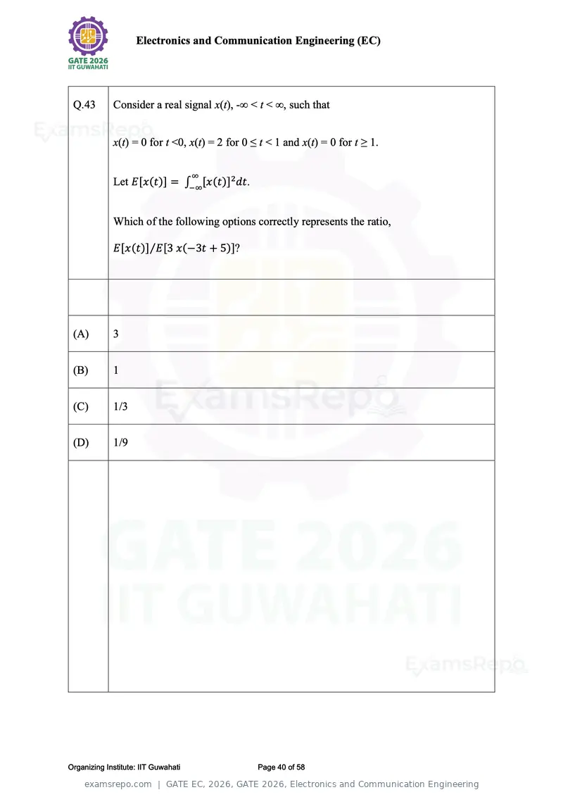
Text of page 40
Electronics and Communication Engineering (EC)


 Q.43        Consider a real signal x(t), -∞ < t < ∞, such that


             x(t) = 0 for t <0, x(t) = 2 for 0 ≤ t < 1 and x(t) = 0 for t ≥ 1.

                                     ∞
             Let E[x(t)] = ∫−∞[x(t)]2 dt.


             Which of the following options correctly represents the ratio,

             E[x(t)]⁄E[3 x(−3t + 5)]?


 (A)         3


 (B)         1


 (C)         1/3


 (D)         1/9


Organizing Institute: IIT Guwahati              Page 40 of 58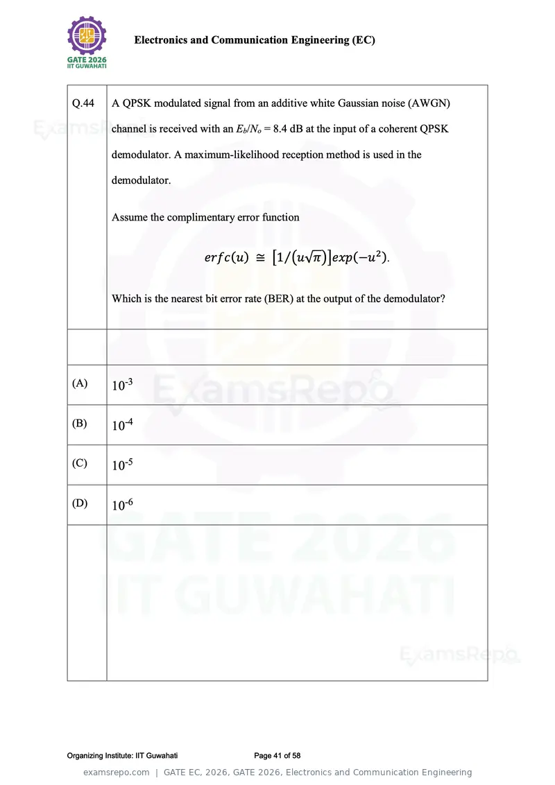
Text of page 41
Electronics and Communication Engineering (EC)


 Q.44        A QPSK modulated signal from an additive white Gaussian noise (AWGN)

             channel is received with an Eb/No = 8.4 dB at the input of a coherent QPSK

             demodulator. A maximum-likelihood reception method is used in the

             demodulator.


             Assume the complimentary error function


                                     erfc(u) ≅ [1⁄(u√π)]exp(−u2 ).


             Which is the nearest bit error rate (BER) at the output of the demodulator?


 (A)         10-3

 (B)         10-4

 (C)         10-5

 (D)         10-6


Organizing Institute: IIT Guwahati           Page 41 of 58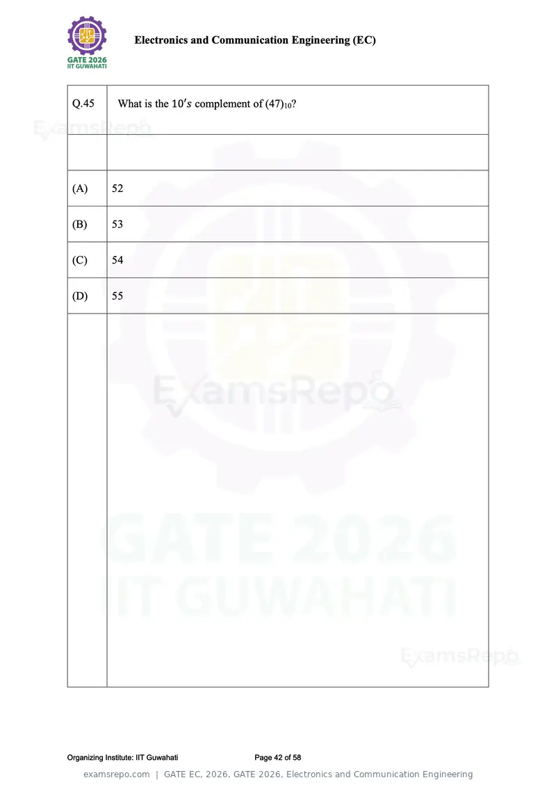
Text of page 42
Electronics and Communication Engineering (EC)


 Q.45          What is the 10′s complement of (47)10?


 (A)         52


 (B)         53


 (C)         54


 (D)         55


Organizing Institute: IIT Guwahati          Page 42 of 58
Text of page 43
Electronics and Communication Engineering (EC)


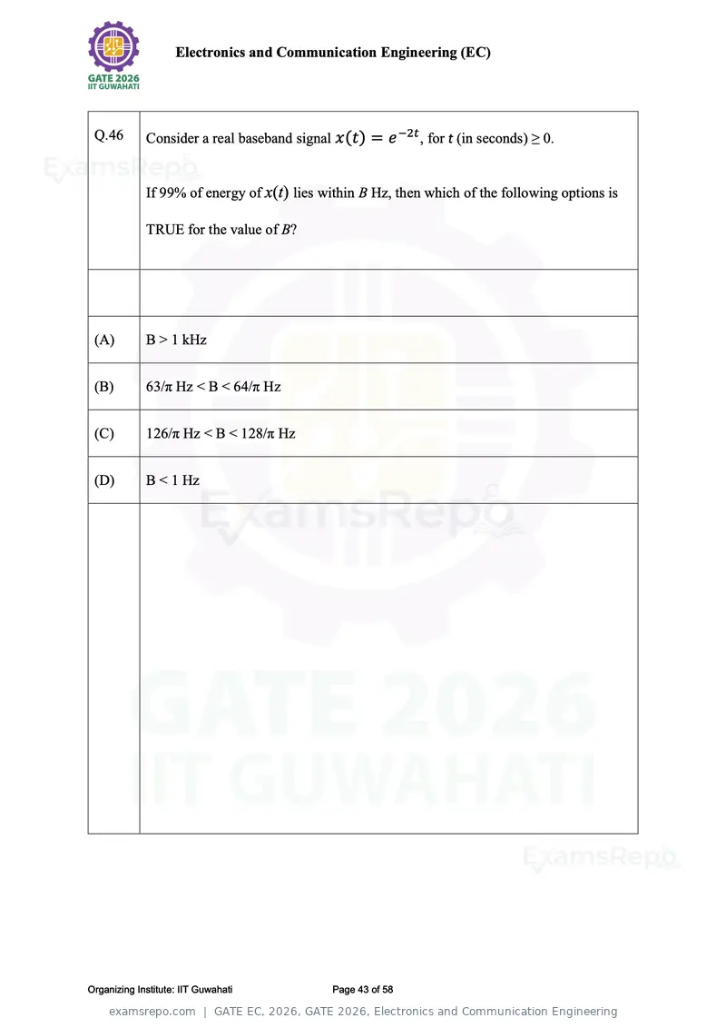
 Q.46        Consider a real baseband signal x(t) = e −2t , for t (in seconds) ≥ 0.


             If 99% of energy of x(t) lies within B Hz, then which of the following options is

             TRUE for the value of B?


 (A)         B > 1 kHz


 (B)         63/π Hz < B < 64/π Hz


 (C)         126/π Hz < B < 128/π Hz


 (D)         B < 1 Hz


Organizing Institute: IIT Guwahati          Page 43 of 58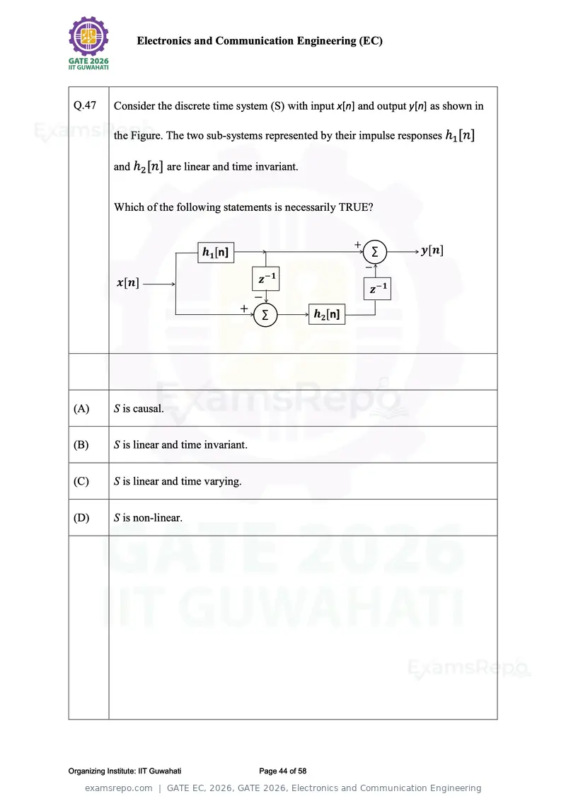
Text of page 44
Electronics and Communication Engineering (EC)


 Q.47        Consider the discrete time system (S) with input x[n] and output y[n] as shown in

             the Figure. The two sub-systems represented by their impulse responses ℎ1 [n]

             and ℎ2 [n] are linear and time invariant.


             Which of the following statements is necessarily TRUE?


                                     n]                              ∑


                                               ∑               n]


 (A)         S is causal.


 (B)         S is linear and time invariant.


 (C)         S is linear and time varying.


 (D)         S is non-linear.


Organizing Institute: IIT Guwahati             Page 44 of 58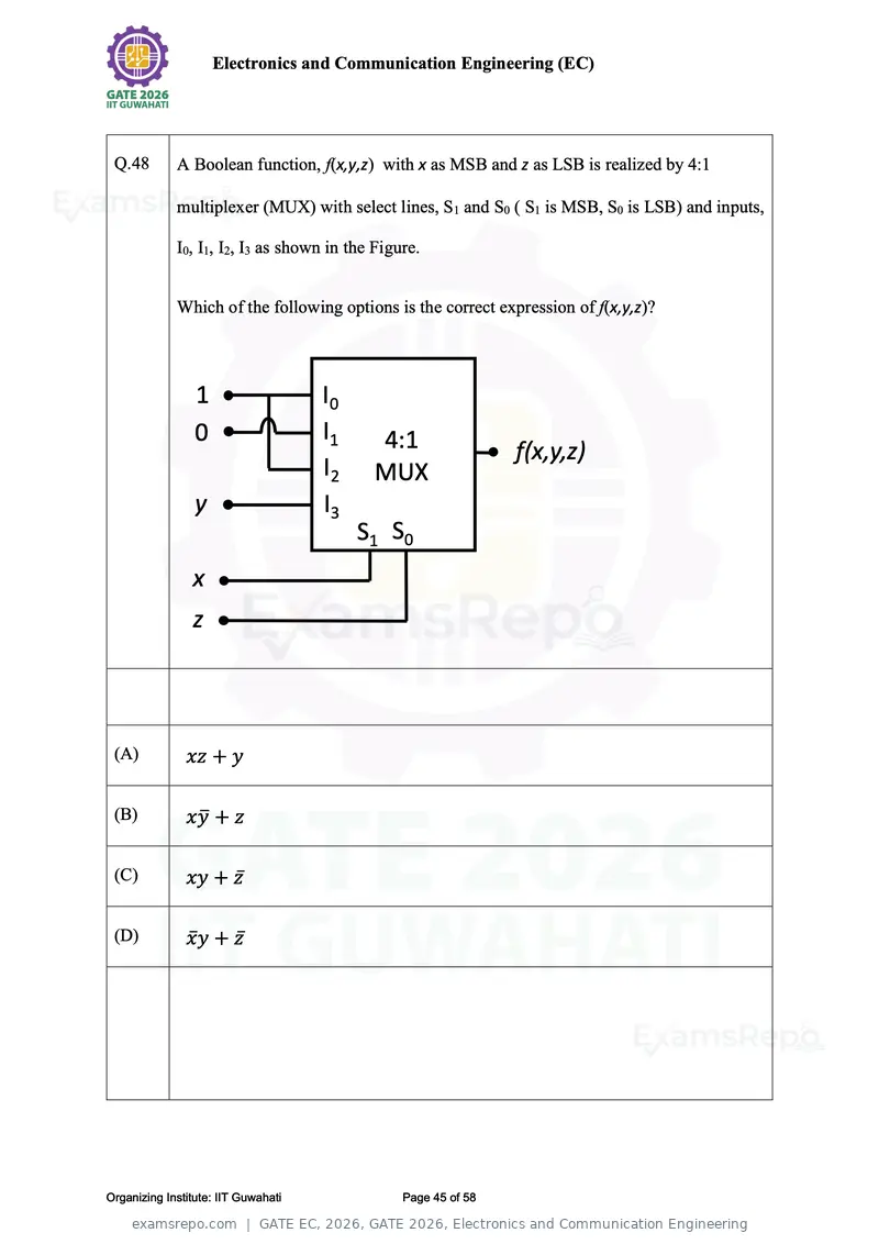
Text of page 45
Electronics and Communication Engineering (EC)


 Q.48        A Boolean function, f(x,y,z) with x as MSB and z as LSB is realized by 4:1

             multiplexer (MUX) with select lines, S1 and S0 ( S1 is MSB, S0 is LSB) and inputs,

             I0, I1, I2, I3 as shown in the Figure.


             Which of the following options is the correct expression of f(x,y,z)?


                 1                   I0
                 0                   I1    4:1                  f(x,y,z)
                                     I2    MUX
                 y                   I3
                                          S1 S0
                x
                z


 (A)           xz + y

 (B)           xy̅ + z

 (C)           xy + z̅

 (D)           x̅ y + z̅


Organizing Institute: IIT Guwahati              Page 45 of 58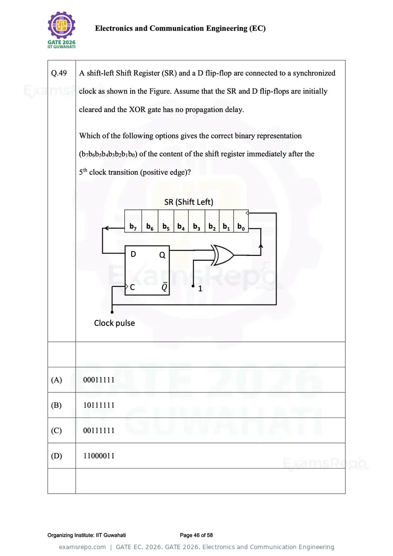
Text of page 46
Electronics and Communication Engineering (EC)


 Q.49        A shift-left Shift Register (SR) and a D flip-flop are connected to a synchronized

             clock as shown in the Figure. Assume that the SR and D flip-flops are initially

             cleared and the XOR gate has no propagation delay.


             Which of the following options gives the correct binary representation

             (b7b6b5b4b3b2b1b0) of the content of the shift register immediately after the

             5th clock transition (positive edge)?


                                               SR (Shift Left)

                                     b7   b6   b5 b4    b3    b2 b1 b0


                                     D         Q


                                     C         ̅          1


                    Clock pulse


 (A)           00011111


 (B)           10111111


 (C)           00111111


 (D)           11000011


Organizing Institute: IIT Guwahati                 Page 46 of 58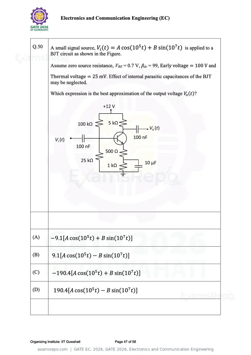
Text of page 47
Electronics and Communication Engineering (EC)


 Q.50        A small signal source, Vi (t) = A cos(105 t) + B sin(107 t) is applied to a
             BJT circuit as shown in the Figure.

             Assume zero source resistance, VBE = 0.7 V, βdc = 99, Early voltage = 100 V and

             Thermal voltage = 25 mV. Effect of internal parasitic capacitances of the BJT
             may be neglected.

             Which expression is the best approximation of the output voltage Vo (t)?


 (A)         −9.1[A cos(105 t) + B sin(107 t)]

 (B)          9.1[A cos(105 t) − B sin(107 t)]

 (C)          −190.4[A cos(105 t) + B sin(107 t)]

 (D)           190.4[A cos(105 t) − B sin(107 t)]


Organizing Institute: IIT Guwahati          Page 47 of 58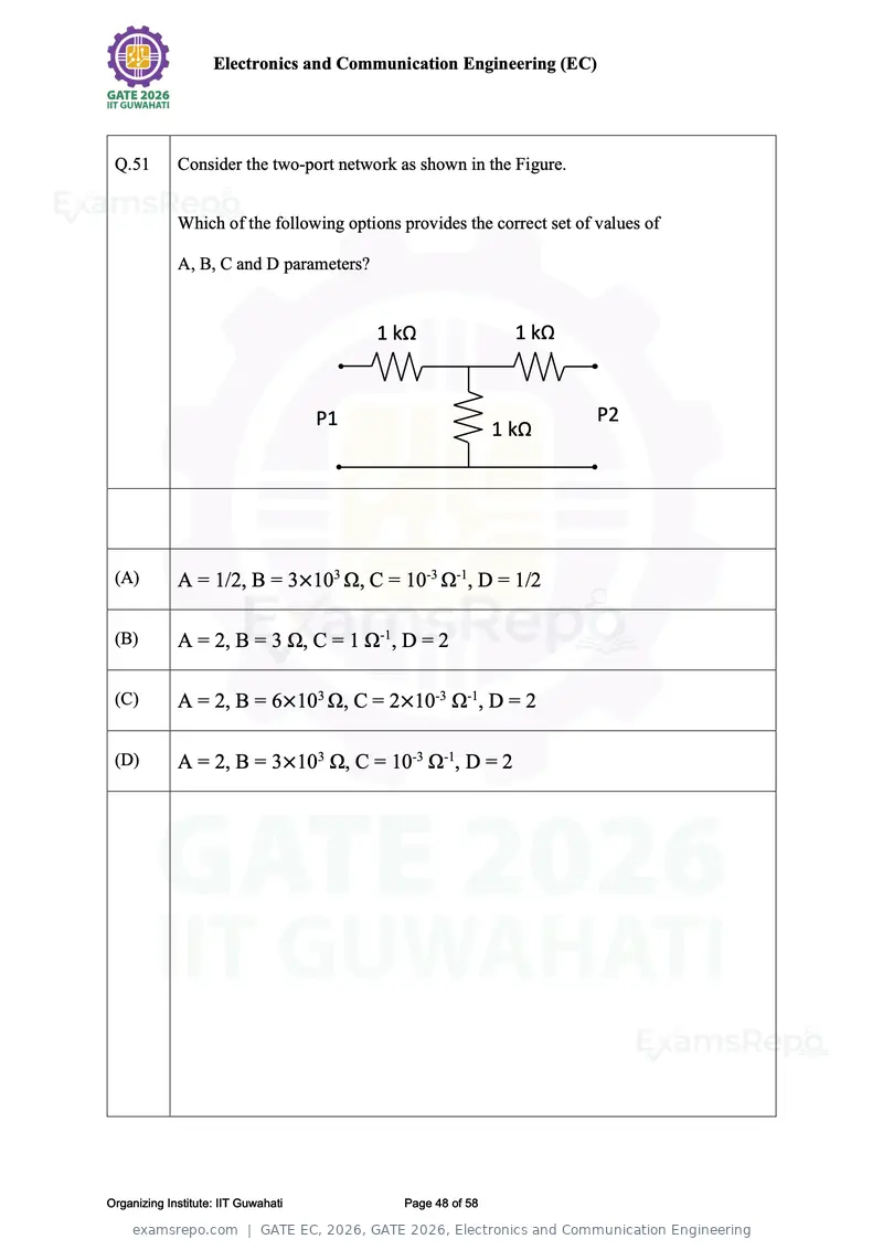
Text of page 48
Electronics and Communication Engineering (EC)


 Q.51        Consider the two-port network as shown in the Figure.


             Which of the following options provides the correct set of values of

             A, B, C and D parameters?


                                          1 kΩ                1 kΩ


                                     P1                                 P2
                                                            1 kΩ


 (A)         A = 1/2, B = 3×10³ Ω, C = 10-3 Ω-1, D = 1/2

 (B)         A = 2, B = 3 Ω, C = 1 Ω-1, D = 2

 (C)         A = 2, B = 6×10³ Ω, C = 2×10⁻³ Ω-1, D = 2

 (D)         A = 2, B = 3×10³ Ω, C = 10-3 Ω-1, D = 2


Organizing Institute: IIT Guwahati          Page 48 of 58
Text of page 49
Electronics and Communication Engineering (EC)


 Q.52        A complex load (in Ω) is represented as ΓL = 0.5∠30o on the Smith chart.

             A co-axial cable with a characteristic impedance of 50 Ω is connected to the load.

             The new input impedance of the load now moves to a diametrically opposite point

             on the same Γ circle on the Smith chart.


             Which option is the nearest input impedance of the cable connected load (in Ω)?


 (A)         20.7 − j5.1


 (B)         17.7 − j11.8


 (C)         97.5 − j65.0


 (D)         97.5 + j65.0


Organizing Institute: IIT Guwahati          Page 49 of 58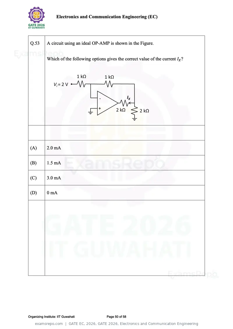
Text of page 50
Electronics and Communication Engineering (EC)


 Q.53        A circuit using an ideal OP-AMP is shown in the Figure.


             Which of the following options gives the correct value of the current IX ?


 (A)         2.0 mA


 (B)         1.5 mA


 (C)         3.0 mA


 (D)         0 mA


Organizing Institute: IIT Guwahati           Page 50 of 58
Text of page 51
Electronics and Communication Engineering (EC)


 Q.54        Consider an LED based on a direct bandgap semiconductor material with energy

             bandgap 1.3 eV.


             Given: Plank’s constant, ℎ = 6.63 × 10⁻³⁴ J s and speed of light in free space is

             3 × 10⁸ m s −1.


             In which of the following wavelength ranges the LED will NOT emit?


 (A)         1410 ± 20 nm


 (B)         1090 ± 20 nm


 (C)         950 ± 20 nm


 (D)         510 ± 20 nm


Organizing Institute: IIT Guwahati           Page 51 of 58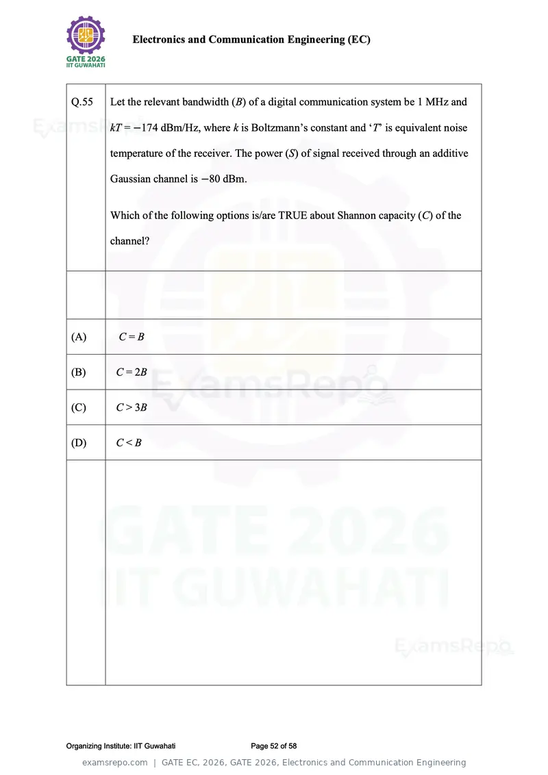
Text of page 52
Electronics and Communication Engineering (EC)


 Q.55        Let the relevant bandwidth (B) of a digital communication system be 1 MHz and

             kT = −174 dBm/Hz, where k is Boltzmann’s constant and ‘T’ is equivalent noise

             temperature of the receiver. The power (S) of signal received through an additive

             Gaussian channel is −80 dBm.


             Which of the following options is/are TRUE about Shannon capacity (C) of the

             channel?


 (A)            C=B


 (B)           C = 2B


 (C)           C > 3B


 (D)           C<B


Organizing Institute: IIT Guwahati          Page 52 of 58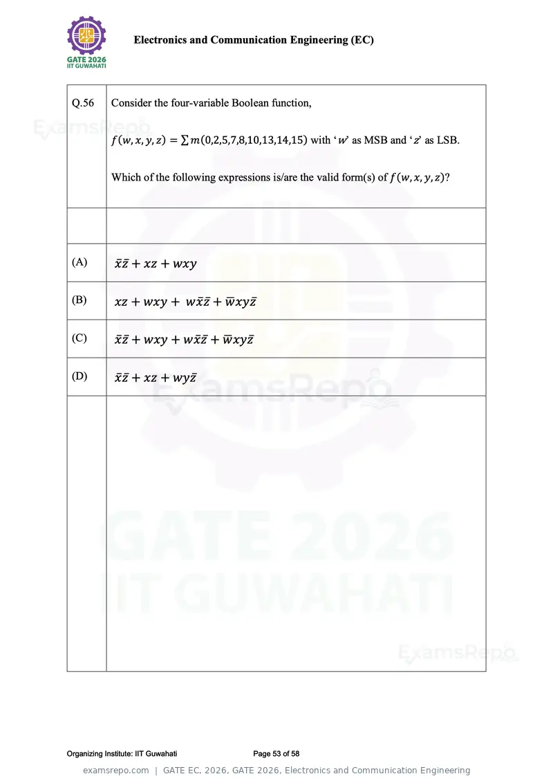
Text of page 53
Electronics and Communication Engineering (EC)


 Q.56        Consider the four-variable Boolean function,


             f(w, x, y, z) = ∑ m(0,2,5,7,8,10,13,14,15) with ‘w’ as MSB and ‘z’ as LSB.


             Which of the following expressions is/are the valid form(s) of f(w, x, y, z)?


 (A)          x̅ z̅ + xz + wxy

 (B)          xz + wxy + wx̅ z̅ + wxyz̅

 (C)          x̅ z̅ + wxy + wx̅ z̅ + w xyz̅

 (D)          x̅ z̅ + xz + wyz̅


Organizing Institute: IIT Guwahati           Page 53 of 58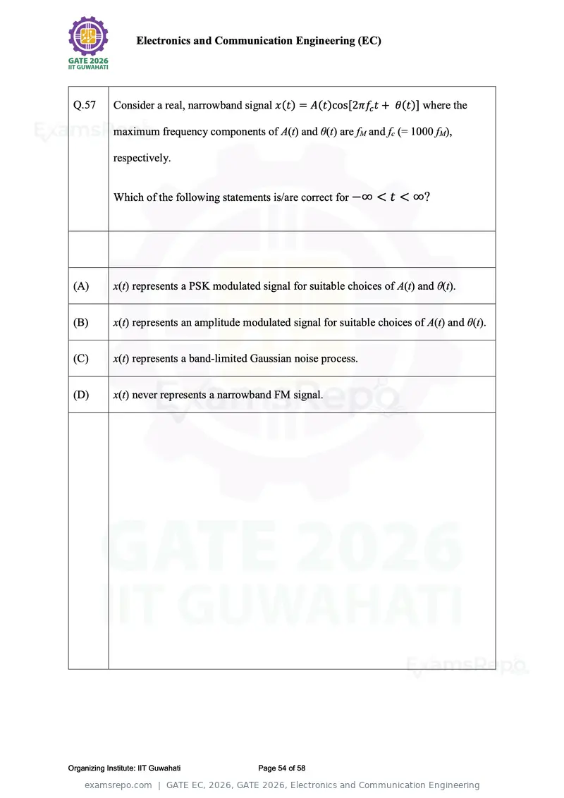
Text of page 54
Electronics and Communication Engineering (EC)


 Q.57        Consider a real, narrowband signal x(t) = A(t)cos[2πfc t + θ(t)] where the

             maximum frequency components of A(t) and θ(t) are fM and fc (= 1000 fM),

             respectively.


             Which of the following statements is/are correct for −∞ < t < ∞?


 (A)         x(t) represents a PSK modulated signal for suitable choices of A(t) and θ(t).


 (B)         x(t) represents an amplitude modulated signal for suitable choices of A(t) and θ(t).


 (C)         x(t) represents a band-limited Gaussian noise process.


 (D)         x(t) never represents a narrowband FM signal.


Organizing Institute: IIT Guwahati           Page 54 of 58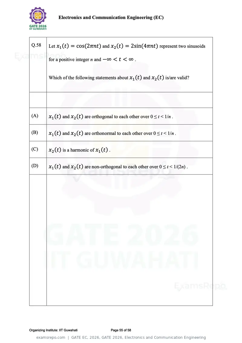
Text of page 55
Electronics and Communication Engineering (EC)


 Q.58        Let x1 (t) = cos(2πnt) and x2 (t) = 2sin(4πnt) represent two sinusoids

             for a positive integer n and −∞ < t < ∞ .


             Which of the following statements about x1 (t) and x2 (t) is/are valid?


 (A)         x1 (t) and x2 (t) are orthogonal to each other over 0 ≤ t < 1/n .

 (B)         x1 (t) and x2 (t) are orthonormal to each other over 0 ≤ t < 1/n .

 (C)         x2 (t) is a harmonic of x1 (t) .

 (D)         x1 (t) and x2 (t) are non-orthogonal to each other over 0 ≤ t < 1/(2n) .


Organizing Institute: IIT Guwahati              Page 55 of 58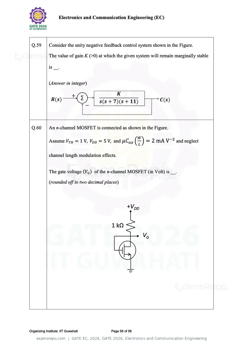
Text of page 56
Electronics and Communication Engineering (EC)


 Q.59        Consider the unity negative feedback control system shown in the Figure.

             The value of gain K (>0) at which the given system will remain marginally stable

             is __.


             (Answer in integer)

                                     ∑


 Q.60        An n-channel MOSFET is connected as shown in the Figure.

                                                            W
             Assume VTH = 1 V, VDD = 5 V, and μCox ( ) = 2 mA V −2 and neglect
                                                            L

             channel length modulation effects.


             The gate voltage (VG ) of the n-channel MOSFET (in Volt) is __.

             (rounded off to two decimal places)


                                                      +VDD

                                            1 kΩ
                                                                VG


Organizing Institute: IIT Guwahati          Page 56 of 58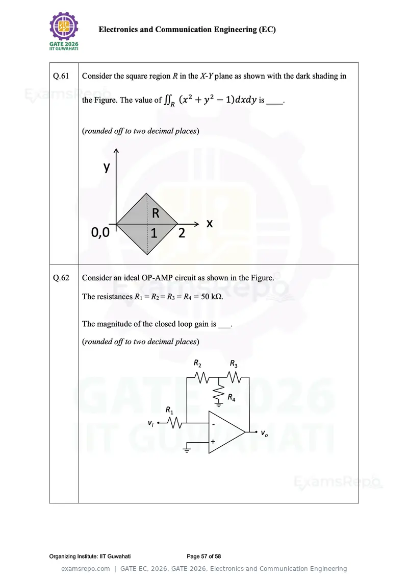
Text of page 57
Electronics and Communication Engineering (EC)


 Q.61        Consider the square region R in the X-Y plane as shown with the dark shading in

             the Figure. The value of ∬R (x 2 + y 2 − 1)dxdy is ____.


             (rounded off to two decimal places)


                      y


                                     R
                                                          x
                 0,0                 1         2

 Q.62        Consider an ideal OP-AMP circuit as shown in the Figure.

             The resistances R1 = R2 = R3 = R4 = 50 kΩ.


             The magnitude of the closed loop gain is ___.

             (rounded off to two decimal places)

                                                     R2            R3


                                                                   R4
                                          R1
                                     vi                     -
                                                                        vo
                                                            +


Organizing Institute: IIT Guwahati                 Page 57 of 58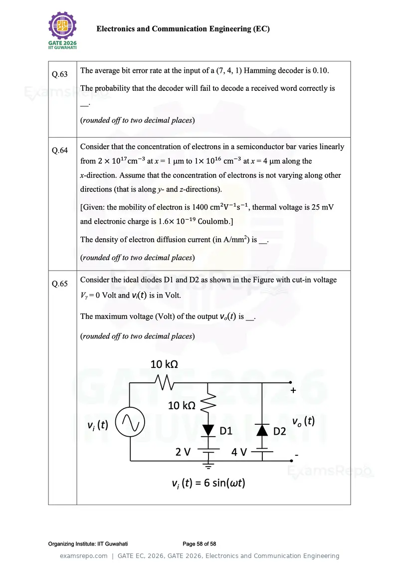
Text of page 58
Electronics and Communication Engineering (EC)
Q.63 The average bit error rate at the input of a (7, 4, 1) Hamming decoder is 0.10.
The probability that the decoder will fail to decode a received word correctly is
__.
(rounded off to two decimal places)
Q.64 Consider that the concentration of electrons in a semiconductor bar varies linearly
from 2 × 1017 cm−3 at x = 1 m to 1× 1016 cm−3 at x = 4 m along the
x-direction. Assume that the concentration of electrons is not varying along other
directions (that is along y- and z-directions).
[Given: the mobility of electron is 1400 cm2 V −1 s−1 , thermal voltage is 25 mV
and electronic charge is 1.6× 10⁻¹⁹ Coulomb.]
The density of electron diffusion current (in A/mm2) is __.
(rounded off to two decimal places)
Q.65 Consider the ideal diodes D1 and D2 as shown in the Figure with cut-in voltage
Vγ = 0 Volt and vi(t) is in Volt.
The maximum voltage (Volt) of the output vo(t) is __.
(rounded off to two decimal places)
10 kΩ
+
10 kΩ
vi (t) vo (t)
D1 D2
2V 4V -
vi (t) = 6 sin(ωt)
Organizing Institute: IIT Guwahati Page 58 of 58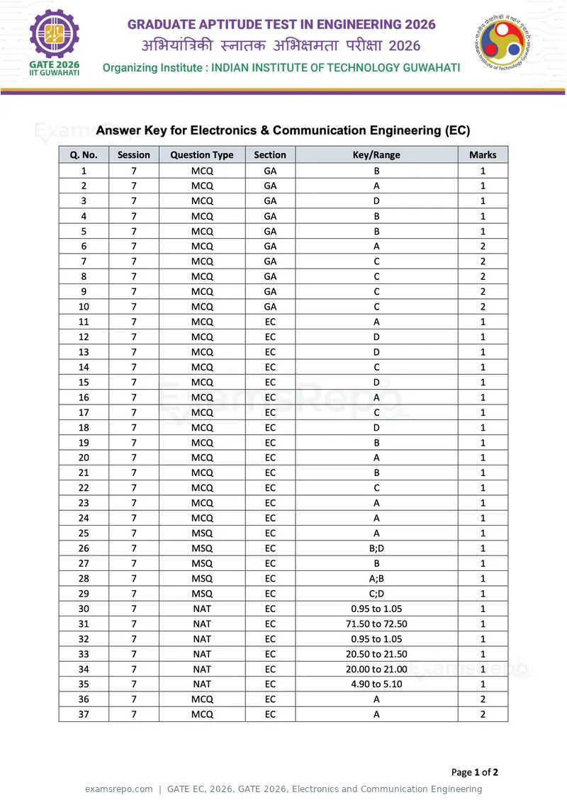
Text of page 1
Answer Key for Electronics & Communication Engineering (EC)
Q. No.   Session   Question Type   Section    Key/Range           Marks
  1        7           MCQ           GA            B                1
  2        7           MCQ           GA            A                1
  3        7           MCQ           GA            D                1
  4        7           MCQ           GA            B                1
  5        7           MCQ           GA            B                1
  6        7           MCQ           GA            A                2
  7        7           MCQ           GA            C                2
  8        7           MCQ           GA            C                2
  9        7           MCQ           GA            C                2
 10        7           MCQ           GA            C                2
 11        7           MCQ           EC            A                1
 12        7           MCQ           EC            D                1
 13        7           MCQ           EC            D                1
 14        7           MCQ           EC            C                1
 15        7           MCQ           EC            D                1
 16        7           MCQ           EC            A                1
 17        7           MCQ           EC            C                1
 18        7           MCQ           EC            D                1
 19        7           MCQ           EC            B                1
 20        7           MCQ           EC            A                1
 21        7           MCQ           EC            B                1
 22        7           MCQ           EC            C                1
 23        7           MCQ           EC            A                1
 24        7           MCQ           EC            A                1
 25        7           MSQ           EC            A                1
 26        7           MSQ           EC           B;D               1
 27        7           MSQ           EC            B                1
 28        7           MSQ           EC           A;B               1
 29        7           MSQ           EC           C;D               1
 30        7           NAT           EC       0.95 to 1.05          1
 31        7           NAT           EC      71.50 to 72.50         1
 32        7           NAT           EC       0.95 to 1.05          1
 33        7           NAT           EC      20.50 to 21.50         1
 34        7           NAT           EC      20.00 to 21.00         1
 35        7           NAT           EC       4.90 to 5.10          1
 36        7           MCQ           EC            A                2
 37        7           MCQ           EC            A                2


                                                              Page 1 of 2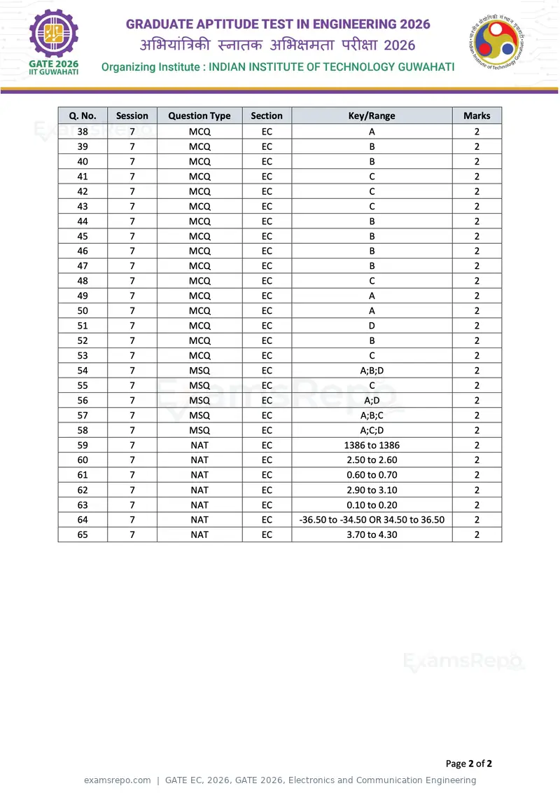
Text of page 2
Q. No.   Session   Question Type   Section              Key/Range                     Marks
 38        7           MCQ           EC                       A                         2
 39        7           MCQ           EC                       B                         2
 40        7           MCQ           EC                       B                         2
 41        7           MCQ           EC                       C                         2
 42        7           MCQ           EC                       C                         2
 43        7           MCQ           EC                       C                         2
 44        7           MCQ           EC                       B                         2
 45        7           MCQ           EC                       B                         2
 46        7           MCQ           EC                       B                         2
 47        7           MCQ           EC                       B                         2
 48        7           MCQ           EC                       C                         2
 49        7           MCQ           EC                       A                         2
 50        7           MCQ           EC                       A                         2
 51        7           MCQ           EC                       D                         2
 52        7           MCQ           EC                       B                         2
 53        7           MCQ           EC                       C                         2
 54        7           MSQ           EC                     A;B;D                       2
 55        7           MSQ           EC                       C                         2
 56        7           MSQ           EC                      A;D                        2
 57        7           MSQ           EC                     A;B;C                       2
 58        7           MSQ           EC                     A;C;D                       2
 59        7           NAT           EC                 1386 to 1386                    2
 60        7           NAT           EC                  2.50 to 2.60                   2
 61        7           NAT           EC                  0.60 to 0.70                   2
 62        7           NAT           EC                  2.90 to 3.10                   2
 63        7           NAT           EC                  0.10 to 0.20                   2
 64        7           NAT           EC      -36.50 to -34.50 OR 34.50 to 36.50         2
 65        7           NAT           EC                  3.70 to 4.30                   2


                                                                                  Page 2 of 2
Page 1 of 58
Source: GATE. Question paper published by GATE.