
MP SET 2022: State Eligibility Test, Electronic Sciences
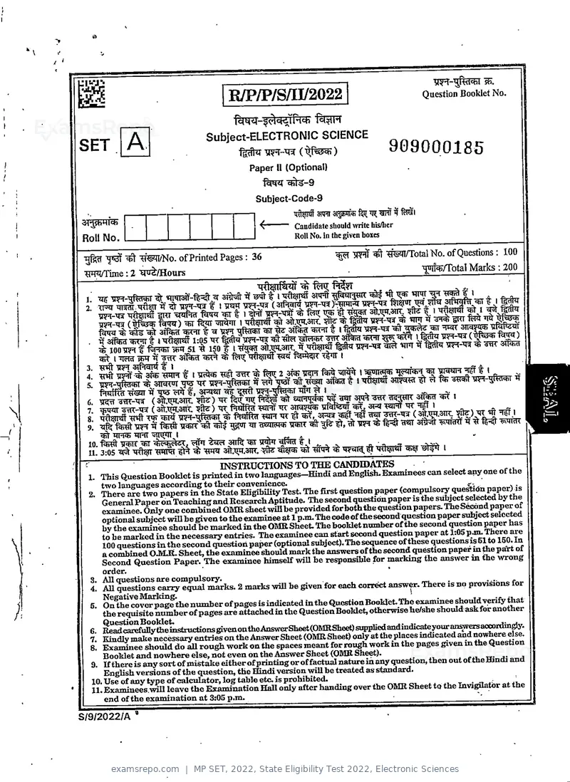
Text of page 1
WP/PISfUJ2022                                                     Question Booklet No.


                                           Subject-ELECTRONIC SCIENCE
    SET                                          ■f^[#ET            ( i^r^ch )                  909000185
                                                    Paper 11 (Optional)
                                                           IciM^
                                                      Subject-Code-9
                                                                         am                ^^
    ar^wg;                                                     ~ Candidate should >vrite his/her
    Roll No.                                                     Roll No. in the given boxes

                                                                                         git wn/Total No. of Questions: 100
                    TP^/No. of Printed Pages : 36
     TlWrime: 2 tpJ^/Hours                                                                                      tpTifgr/Total Marks: 200


        ^         -Ljwi ^ 1 uiiMTgff 1*05 TITfeatg TRT-qr      'dtn "otviqiT     Sifiu «n^nj            <t»VM                (,               -r ^
       ^ 1 TRTg wr "aj^ atfeg cKt% ^           rjt*A<K ^^*11 1
     4                     igto-R^arTT^ to 2 atqT-g^                                                                              Lw^
     5* TiT^-HitoT ■% arra^ ^ g9T--^feraT if                                   3ito11                           ^^            wr-^ftor t
     6. g^'am-TIW ( ^.tTtT.3TTT. T?ftg) ttT                    ^                    ^          ..           ^ Sff?
     7 gnrar ^riT-Tra (ait"TnT.aut. "^fte) tit Iwf^ T«rnt tit aira?^                    ^                 ^ W ' __ „_)-qT^1^1
\
        ^ Ting) TIHT Miiiiqi 1       ^                              ,
     10. "f^vdt iraiT ■qjT 4ic«h^<iT. WT      3TTR qn" hmIm         ^1 ft. ^            jl •               . ., -4v^ i
     11. 3:05 ^ Ttftastr TWntt           Wt afr.Trq.aiR. ^          ^ Tlfq% ^                             ^          '
                                             ESfSTRUCTIONS TO THE CANDIDATES
        This QuestionBooklet is printedin two languages-Hindi andEn^h.Examinees can select any one of the
        two lanffuages according to their convenience.                                            o
        There are two papers in the State Eligibility Test. The first question paper (comp^soiy qu^dnpaper) as
        GeneralPaper on Teaching andResearch Aptitude. The second qu^onpaper is the
        examinee. Only one combined OMR sheet wiHbe provided for boththe questionpapers. The          paper of
        optional subject wiUbe given to the examinee at1p.m. The code of the s^ndquestionpaper ^ject
         by the examinee shouldbe markedin the OMR Sheet. The bookletnumber ofthe se<»nd^estionpaper has
         to be markedin the necessary entries. The examinee can start second question paper at 1:05
         100 questions inthe second questionpaper (optional subject). The sequence ofthese questionsis 51to 15^1^
         a combined OJMJt Sheet, the examinee should mark the answers of the second questionpaper m^e          of
         Second Question Paper. The examinee himself will be responsible for marking the answer m the wrong
         order.
         All ouestions are compulsory.                                                                          ^        .        • ■•■
         All questions carry equal marks. 2 marks will be given for each correct answer. There is no provisions for
         On^he cover page the number ofpages isindicatedinthe QuestionBooklet.The examinee shouldverify that
;        the requisite number of pages are attachedin the QuestionBooklet, otherwise he/she should ask for another
         QuestionBooklet.
      6.
      7. Kmdly maae necessary entnesuuvue Auawisi.                                                                                        ^      ^
      8. Examinee should do all rou^ work on the spaces meant for rough work m the pages givenm the Question
         Booklet and nowhere else, not even on the Answer Sheet (OMRShwt).                                e.u^x3i„Ai
      9. If there is any sort of mistake either ofprinting or of factual nature m any question, then out ofthe Binoi ana
          English versions of the question, the Hindi versionmilbe treated as standard.
      10, Use of any type of calculator, log table etc. is prohibited.                                 t • i a ' **i.
      11.Examinees.will leave the Examination HaR only after handing over the OMR Sheet to theInvi^tor at the
         end of the examination at 3rf)5 p.m.                                                       '
    S/9/2022/A
Text of page 2
)*


             (SPACE FOR ROUGH WORK)


S/9/2022/A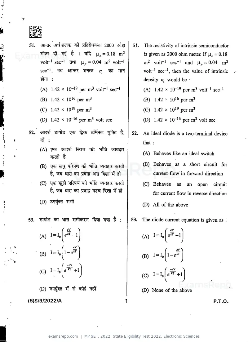
Text of page 3
51.                                   ^                 2000 ^ 51. The resistivity of intrinsic semiconducfor
            1—c
              ^ TTf t i "^Tf^ |l, =0.18 m2
                  II                                                        is given as 2000 ohm meter. If p.^ = 0.18
                       1—<o
       volr' sec~'                           |j.^ = 0.04 ni- volr'          m^ volt"' sec"' and p.^ = 0.04
      sec"',                      a-TRp; w\^             ^ iirr             volt"' sec"', then the value of intrinsic           «.'
            :                                                               density         would be *

      (A) 1.42 X 10~^^ per m^ volr' sec"'                                  (A) 1.42 X 10~'9 per m^ volr' see"'
      (B) 1.42 X lO'^-per m3                                               (B) 1.42          10'^ per
      (C) 1,42 X 10¹⁹ pei- jn3                                             (G) 1.42 X 10'9 per m^
      (D) 1.42 X 10"'^ per                          volt sec               (D) 1.42 X 10"'^ per m^ volt sec

52.                                TT^                         f,    52.    An ideal diode is a two-terminal device
      ^:
                                                                           that ;
      (A)                                                  OMCI6K
                                                                           (A) Behaves like an ideal switch
                              t
      (B)     ^       ^^ oijci^K wt                                        (B) Behaves as a short circuit for

            t,^ ?iRi ^ 31^ sm    ^                                               current flow"in forward direction

      (C)     ^   ^^                                                       (C) Behaves           as       an   open   circuit
            t,^ ^ 31^                                          ^                 for current flow in reverse direction

      (D)                         "?T^                                     (D) All of the above


53.           ^ TO ^h14i<ui                            "TO f :       53. The diode current equation is given as :
                              ^ eV       >                                              / eV        \

      (A)                      e^^-1                                       (A) 1 = ^0 e^-1
                              \          >                                              \           /

                              ^       eV^
                                                                                        f"       £y>
      (B) I = Io 1-e^"^                                                    (B)   I= L       1-e^T
                              L          >                                              \           /
                              f -eV
                                      +1                                                f' -eV        ^
      (C) I = Io
                                                                           (C)   I = L e^^T+l
                                                                                        V             /


      (D) "STl^                      ^ ^^                                  (D) None of the above

(5)S/9/2022/A                                                                                                         P.T.O.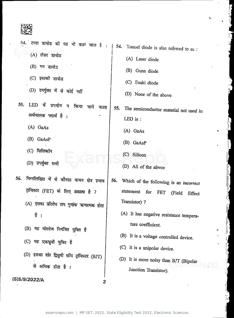
Text of page 4
^4.                     ^ ^ ^ ^^ f .
                                                           54. luruiel diode is also refeaed to as :
         (A)^
                                                               (A) Laser diode
         (B) Tpr
                                                               (B) Gunn diode
         (C)               ^rqte
                                                               (C) Esaki diode
         (D) <SH^CW
                                                               (D) None of the above

  55. LED t)' wfhr                           ;3jtH ^
                                                          55. The semiconductor material not used in
         3T4-qi(ri<^ "^T^af f ;
                                                               LED is :

        (A) GaAs
                                                              (A) GaAs
        (B) GaAsP
                                                              (B) GaAsP
        (C) f^Tf^
                                                              (C) Silicon
       (D)
                                                             (D) All of the abvoe

 56.                       ^                 ^           56, Which of the following is an incorrect
                (FET) ^ %TT 37^ t ?                          statement for FET (Field Effect

       (A)                     ^ ;^uiict) '^u||^ch           Transistor) ?

             t I                                             (A) It has negative resistance tempera
                                                                  ture coefficient.
       (B)                                 f
                                                            (B) It is a voltage controlled device.
       (C)      "0^7^               t
                                                            (C) It is a unipolar device.
       (D)         "^il^           "^ff^ diTslWI (BJT)
                                                            (D) It is more noisy than BJT (Bipolar
             ^ 3TfTO ^ t I
                                                                 Junction Transistor).
(5JS/9/2022/A
Text of page 5
57.                  (CNT)^             f^^Peif^d    57.     Which of the following is /nve for CNT
                                                            (Carbon Nanotubes) ?
                                             >
                                                            ' (A) Strength of CNT is 100 times that
      (A) CNT ^                       ^ ion
                                                                 of steel
            37fe t
                                                            (B) CNT         has   inferior   thermal
      (B) CNT ^                       ^M<4idl t                  conductivity

      (C) CNT ^ 31Tf^W^ Tl\ 2005 ^ ISTT                     (C) CNT was discovered in year 2005

      (D)          "^f     ^                                (D) None of the above

58.                  JFET ^ 3#t^kR 5FiW              58.    The maximum transconductance for a

                                                            certain ^-channel JFET 3.5       ms. If
      ■ciiei=tiai 3.5 ms ^ I      Ij^gg = 25 mA,
      cK ^*g,^rii qlcxai          :                         Idss ~ 25 mA, then the pinch off voltage
                                                            would be :
      (t^ ^ I^gg                       "I,
                                                           . (Given I^gs is drain current when gate
      ^                    t) I                             source voltage is zero).
      (A) - 142.9                                           (A) - 142.9 volt
      (B) - 7.145 ^ .                                       (B) - 7.145 volt

      (C) - 14.29 ^                                         (C) - 14.29 volt

      (D) - 28.58 ^                                         (D) - 28.58 volt


59.          ^ ■Q=fT HMet ^                          59.    A quantum well is 2D nanomaterial

      f, 1^* :                                              structure having :

      (A) iqcrl             ^         ^          f          (A) Only one dimension in nano range

      (B) ^                 M^ ^ f                          (B) Two dimensions in nano range

      (C) ^ #1              ^ M^ ^ t                        (C) All three dimensions in nano range

      (D)                  ^ "q^*                           (D) None of the above

(5)S/9/2022/A                                                                                 P.T.O.
Text of page 6
60.                      ^       -qcf          ^     60. The orientation of molecules in a 4ayer
                     ^        3TRffqcr ^        ^          of liquid crystal can be changed by
        ti^ai ■ % ■: "                                     applying :

        (A)                                                (A) Magnetic field

        (B)                 ^                              (B) Electromagnetic field

        (C) 1^ ^                                           (C) Electric field

        (D) 3M^ckl          ^                             (D) None of the above

61.                               ^^ t ?             61. Which design approach takes less space ?
       (A) <rl^«t t^m                                     (A) Lambda rules

       (B) '^l^shln "fWT                                  (B) Micron rules

       (C) w fm                                           (C) Layer rules

       (D) ^                                              (D) Source rules


62.                      ^ aqrojs          "q^ cT^   62. During the logic 1 to 0 transition at the
       1 ^ 0 'mm ^ ^kR                                    output    node     of   CMOS-Invertor,
       ^ t :                                              capacitance discharge is through :
       (A) -^R-STq TTf^?T                                 (A) Pull-up resistance path

       (B)                          ^                     (B) Pull-down resistance path

       (C)                 '■^-•^\^ #ff -hM^i            (C) Both       Pull-up   and   Pull-down
              TR^                                             resistance path

       (D)      ciWdd ^ "RTSIRT ^                        (D) GATE terminal

(5)S/9/2022/A
Text of page 8
65. What is the resistance of a base diffused
         150 jim '^% 4-st^ 10 /jm f I ^                  resistor having a length of 150 (am and
                  W TlfM^ 100               t,           width of 10 pm, if its sheet resistance is
        ^            ^ 1TH ■^trjT .                      100 Q/square ?

        (A) 500 12             (B) 1000 Q                (A) 500 Q            (B) 1000 Q.

        (C) 15oOn              (D) 2000 n                (C) 1500 n           (D) 2000 n

 66.                tllVi f^TTrhr '4* tl|^e^<U|    66. The main purpose of metallization in
                       ^               f .              fabrication of IC is :

        (A)                                 ^           (A) To protect the chip from oxidation

       (B)            -^rf^ tT^* ^ 3^yxj^ ■^'           (B) To     interconnect     the   various

                                                             components of the circuit

       (C) itz 1^            ^ ii ^ ^                   (C) To act as a heat sink

       (D)                 ^ ^ -JT^*                    (D) None of the above

67.           ^iWT          'n' ^811   "a^ ^
                                                   67. What type of line separates the       and
       ■^rf^R^ ^ 1^ "a^                     31OT
                                                        y type transistor in stick diagram ?
              ^TIclT ^ ?
                                                       (A) Black line
       (A) «hi(n1
                                                       (B) Demarcation line
       (B)             cTTf^

       (C) TT^r                                        (C) Arrow line

       (D) "sa^        ^                               (D) None of the above

(5)S/9/2022/A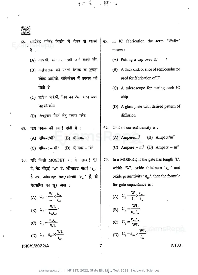
Text of page 9
ir! •


68.                                             ~<^'^ I fj^'. In IC fabrication the term 'Wafer
                                                                   means:


      (A)                               ^         ^                (A) Putting a cap over IC          "

      (B)               ^ Hciefl fs^             i^nsi             (B) A thick disk or slice of semiconductor

                                            Wk ^                         used for fabrication of IC

                   t                                               (C) A microscope for testing each IC

      (C) MCHcti                1kT ^             cilCil                 chip

                                                                   (D) A glass plate with desired pattern of

      (D)                           'QIW                                 difilision


69. TO TO^-                             "I" :              69. Unit of current density is :

      (A)                         (B)                              (A) Ampere/m^            (B) Ampere/m^

      (C)                         (D) ^^pW-k2                      (C) Ampere - m^ (D) Ampere - ra^

70.         1^ MOSFET ^ k eraf 'U                          70. In a MOSFET, if the gate has length *L\

      tk               'W' t,               ■rtelf 'tj             width 'W', oxide thickness              and

      t cI8?T 3iT=HHI^^                    'e^' %, eft             oxide permittivity '       then the formula

      fti^lRdl ^ ^ #n :                                            for gate capacitance is :


      (A) C.=-x^
            L  r
                   W        e
                                                                   (A) C.=^x^
                                                                         L  L

                   WL                                                           WL
                                                                         C =
      (B) c.=                                                      (B)
                                                                                ^Jox
                   ^ox^ox

      (C)                                                          (C)
                   WL
                            V/L                                                        WL
      (D) C,=e^x                                                   (D) Cg=eaxX

(5)S/9/2022/A                                                                                             P.T.O,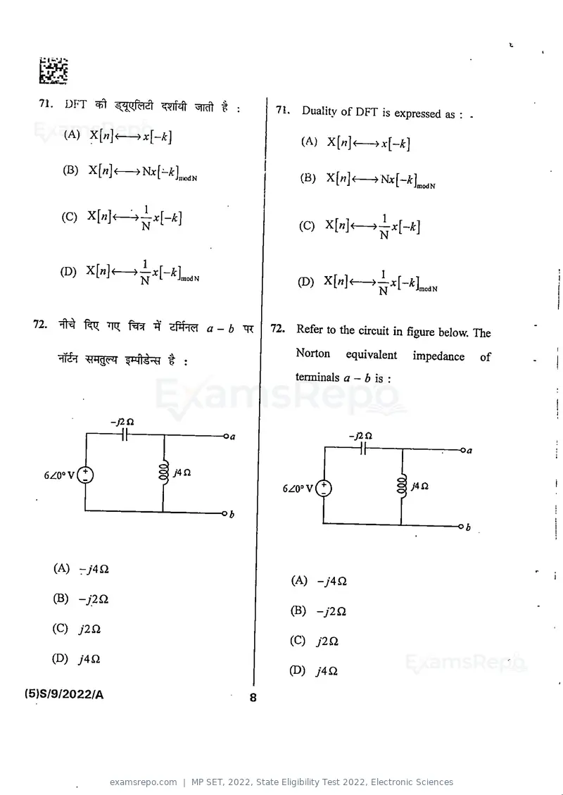
Text of page 11
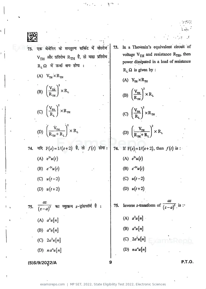
73.                  ^                         73. In a Thevenin's equivalent circuit of
                                                    voltage ^TH and resistance R-j^, then
      ^TH                   ^XH   ^   yRi^'T
                                                    power dissipated in a load of resistance
      Rl^I                        :
                                                    Rl Q. is given by :
      (•^) ^TH ^^TH
                                                   (^)
            'v-''
               *TH                                               \2
      (B)            xRi.                                 V.TH
            vB-ray                                 (B)                XRl


               ^TH
                     xRTH                                 "m
      (C)                                                             xRTH
            Ul                                     (C)
                                                           Rl

            ^ y*TH Y xRl                                     'TH
      (D)                                          (D)                   XRl
               R.jj,+ Rl^


74. ^ F(j)= 1/(^+2) t, (it /(/) #11: 74. If F(4=1/(s+2), then /(/) is
      (A) e^'uit)                                  (A) e"u{t)
      (B) e-"u{t)                                  (B) e-"u{t)
      (C) u{t-2)                                   (C) «(r-2)

      (D) u{t+2)                                   (D) u{t+2)

                                                                               az
         az-

75. (^z-af ^ ^3^ z-sjrawf t                    75. Inverse z-transform of
                                                                             (z-a),2 IS :

      (A) a^u[n]                                   (A) a^«[n]

      (B) a"u[n]                                   (B) a"K[n]

      (C) 2a^u[n]                                  (C) 2a^a[n]

      (D) na"u\n\                                  (D) na"u[n]

(5)S/9/20?2/A                                                                          P.T.O.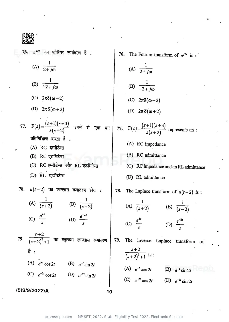
Text of page 12
76. e^'^' ^ 4)1 Rq< "WOT f :                           76. The Fourier transform of               is
                 1
                                                                                1
       (A)
             2+jGi                                               (A) 2+70)

                 1
                                                                                1
       (B) -2+70)
                                                                       -2+yco
       (C) 27c5(o)-2)                                            (C) 27c6(o)-2)
       (D) 23r6(o)+2)                                            (D) 27c6(o) + 2)

                                                         7T
                                                         / /.    rpc«)_             — represents an :
 "■                                 Trt- S        »
                     ch-(.ai t" :
                                                                 (A) RC impedance
       (A) RC
       (B) RC                                                    (B) RC admittance

      (C) RCW^ 3^^ RLT^f^t^                                      (C) RC impedance and an RL admittance
                       I


      (D)        T^sft^                                         (D) RL admittance

 78. u{t--2) ^ eirara                        ^:         78. The Laplace transform of m(/-2) is :
                                                                            1
      (A)   (j+2)              (B)    (^-2)                     (A)   (s + 2)         (B)   (^-2)
                                      .-2j

      (C) —                    (D)                                    ^2s                   --25
             S                         5                        (C) —                 (D)
                                                                                             s

         5+2

      (5 + 2)^ +1 ^                           "OTcR^    79. The inverse Laplace transform of
                                                                   5 +2

                                                                (5+2)Vi
      (A) e"'cos2r             (B) e-'sin2^
                                                                (A) e-'cos2/         (B) e"'sin2f
      (Q e^'cos2/             (D) e*^'sin2/
                                                                (Q e~^'cos2t         (D) e~^'sin2/
(5)S/9/2022/A                                      10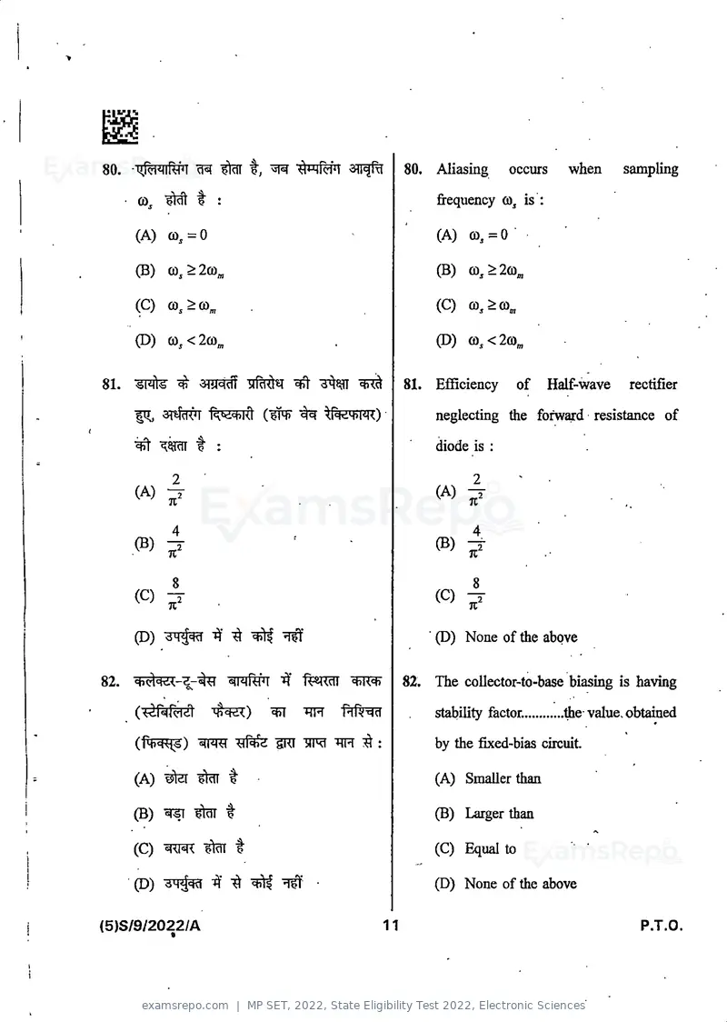
Text of page 13
80. WnRm ^^ t, ^                                    80. Aliasing      occurs    when     sampling

      ■ CO, ^ t :                                        frequency O), is :

      (A) CO, =0                                        (A) o), =0

      (B) co,>2co„                                      (B) a),>2fl)„

      (C) co,>co„                                       (C) co,>©„

      (D) m,<2co„                                       (D) ffl,<2©„

81.          ^ aro^ nfcRtsi                ^ 81. Efficiency             of   Half-wave   rectifier

            3i^cR0                  ^ Wqim)              neglecting the forward resistance of

      ^               f:                                 diode is :

             2
      (A) rr
            n


            _4
      (B)                                                ®7
             s                                                 8
                                                        (C) -r
                                                               n


      (D)                       ^                       (D) None of the above


82.              Cs
                       ^FTftPT                      82. The collector-to-base biasing is having

                                                         stability factor.     Ae value,obtained

      (to^)                         TIRT iTR   :         by the fixed-bias circuit.

      (A) ^ter             "I                           (A) Smaller than

      (B) ^^ t                                          (B) Larger than

      (C)                   f                           (C) Equal to

      (D)                  ^^         ■                 (D) None of the above

(5)S/9/2022/A                                  11                                          P.T.O.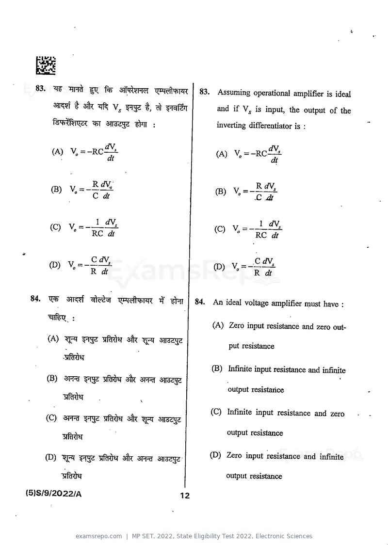
Text of page 14
83.               ^                            83, Assuming operational amplifier is ideal
                                                      and if V^ is input, the output of the
                                                      inverting differentiator is ;

                 dV
        (A) V,=-RC^
                         at
                                                     (A) V, = -RC^
                                                                dV

                                                                       at


        (B) \=--^'
                    C dt


                    1 dV^                                          1 dV^
        (C) V.=-                                     (C) X, = -
                    RC dt                                         RC dt


                                                                  CdV^
                                                     (P) \ = -
                                                                 R dt


 84. 1^ 3TT^ qle^v3l RR^hTiRR "4*               84. An ideal voltage amplifier must have :
        ■qifty; :
                                                    (A) Zero input resistance and zero out
        (A) ^           "ffM?? afk ^
                                                         put resistance


                                                    (B) Infinite input resistance and infinite
    (B)                         3FRr 37T3235
                                                         output resistance
            3iM«i               ^
                                                    (C) Infinite input resistance and zero
    (C)                       sSk ^ 3^555
                                                         output resistance
            3rM?T

    (D)              "SM^T 3^ 37TO 3T[^H52          (D) Zero input resistance and infinite

            "sjM^                                        output resistance

(5)S/9/2022/A                              12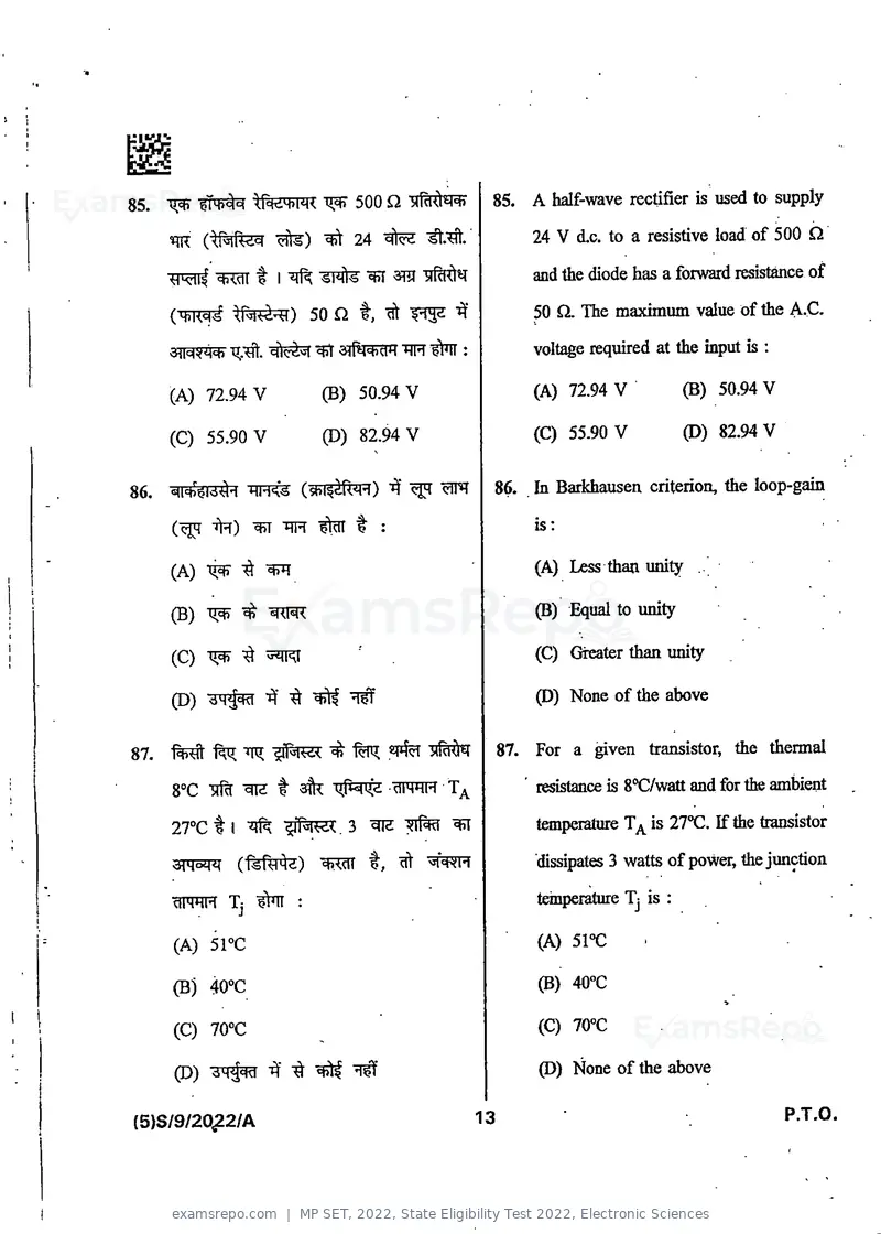
Text of page 15
85. "0^                             500 Q            85. A half-wave rectifier is used to supply

      ^                 ete) ^ 24 ciW ■^.^.                  24 V (Lc. to a resistive load of 500 Q

                      t I               ^ 3m 3iMv            and the diode has a forward resist^ce of

      (T?n^                  50 n t eft W                    50 f2. The maximum value of the A.C.

                                                             voltage required at the input is :

      (A) 72.94 V             (B) 50.94 V                    (A) 72.94 V           (B) 50.94 V

      (C) 55.90 V             (D) 82.94 V                    (C) 55.90 V           (D) 82.94 V

86.                         (sbl^iPWH)               86. In Barichausen criterion, the loop-gain

                                                             is:
      (^5         ^ HH ^Icit ^ :
      (A)                                                    (A) Less than unity ..

      (B)         ^                                          (B) Equal to unity

      (C)         ^                                          (C) Greater than unity

      (D) <44^*^             "^ftf 'l^T                      (D) None of the above


87. -M i^ ^                    ^ tR «PfcT                87. For a ^ven transistor, the thermal
      8°C "afer         t 3k "Qp^ -WWT T^                    resistance is 8'X^/watt and for the ambient

      27°C t I ^                    3          ^             temperature     is 27°C. If the transistor
      3PI5zt^ ("fM^rftz)                t, ^                 dissipates 3 watts of power, the junction

      mwr Tj #11 :                                           temperature Tj is :

      (A) SVC                                                (A) 5l°C

      (B) 40'^C                                              (B) 40°C

      (C) 70°C                                               (C) 7(rC

      (D) dM^«Kl             ^ftf                            (D) None of the above

(5)S/9/20^2/A                                       13                                            P.T.O.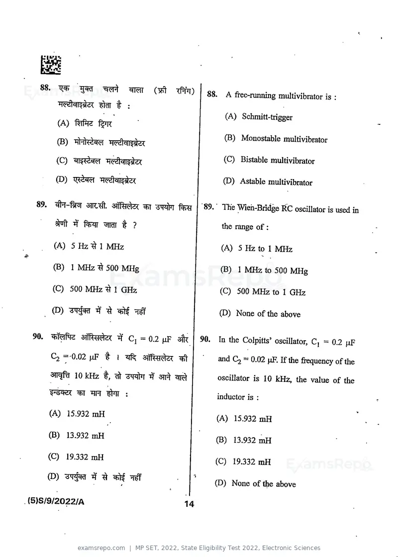
Text of page 17
91.       TOT ^                                ^t        91. Which type of memory is non-volatile

                    ^            ^ ^ 3TOT OT                  and retains its data even when the power

      TORR Tl^ t ?                                            is turned off ?


      (A) RAM                                                 (A) RAM

      (B) ROM                                                 (B) ROM

      (C) DRAM                                                (C) DRAM

      (D) EEPROM                                              (D) EEPROM


92.       3-fe i<HlelH! ^                                92, A 3-bit analog to digital converter is

      y.llQlMI iTFT^ ^                         1^             designed to .digitize analog signals

              "f^RTT ■'RTT "t,        RTRT 0                  ranging from 0 V to 10 V. For this

        10.          t I ITT               ^    6             converter     the     binary      output

          I^ ^                       airjdgs ^:               corresponding to an input of 6 V is :

      (A) Oil                    (B) 101                      (A) Oil             (B) 101

      (C) 100                    (D) 010                      (C) 100             (D) 010


93. IW Ti^R^T ■^*                  ^ i^JTO "OTTh         93. In shift register, serial data can be
      ^R^ TTtft^ ^ ^ TlHHIcK ^ ■4'                            converted into parallel data by using :
                       "=511 ^TOTT f ?
                                                              (A) SIPO
      (A) SIPO
                                                              (B) PISO
      (B) PISO-
                                                              (C) SISO
      (C) SISO

      (D) PIPO                                                (D) PIPO

(5)S/9/2022/A                                       15                                          P.T.O,
Text of page 18
94. Mod-9^^^ ^ I 94. How many minimum number of
             ^ aqmw ^ I flip-flops are required to construct a
      ^'                                           '         Mod-9 coimter ?
     (A) 3                   (B) 9                          (A) 3                    (B) 9

     (C) 10              (D) 4                              (C) 10                  • (D) 4

 95. HDL^                                    ^         95. "Which of thfe FoUo\\ing statements is true
              afe        ^             Pinrdf^d
                                                            regarding the analysis and design of
                                 t ?
                                                            digital circuits using HDL ?
     (A) HDL ^ wjhr                          ^
                                                            (A) HDL is used for simulating and
                                                                 testing digital circuits but not for
                %,                      ^ %IT
         ^ I                                                     their synthesis.

    (B) HDL                                 ^              (B) HDL allows designers to describe

                                                                 the behaviour and structure of
                     ■§■ I
                                                                digital circuits.
    (C) HDL ^                     ^ -^Tri^ ^
                                                           (C) HDL can only be used for small
                             ^              TjTT
                                                                scale digital designs and is not
                t 3%
                         iI
                                                                suitable for complex circuits.

    (D) HDL Wi{^ cRf ^                    ^                0^) HDL is limited to representing
                     f 3^ ST^srfTT^                             combinational logic and cannot
     .               ^           f I                           handle series circuit.

(5)S/9/2022/A                                 16
Text of page 19
96. PHHrdP^d           ^                             96. The state diagram corresponding to the

      t:                                                   following circuit is :


  X                                                    X

  y                                                    y
                    Clock                                                 Clock

                               Flip-Flop                                            Flip-FIop

                      00,01,10                                              00,0.1,10


      (A)                                                  (A)

                      01,10,11                                              01,10,11


                       01,11                                                 01, II


                                  1 L )00, 10                                           1 L )00,10
      (B)                                                  (B).
            00,01                                                 00,01
                        01,11                                                01,11


                                       01,10                                                01,10
      (C) 01,10                                            (C) 01,-10
                      00, 11                                               00, II


      (D)                                                  (D)

                     00, 01,10                                             00, 01,10


(5)S/9/20g2/A                                   17                                           P.T.O.
Text of page 20
97. efff^
                                                        97. The most important parameters for
                                                             evaluating and comparing logic families
        (W), srqoq^ ^ f I pHHRrjRsjd                         are power dissipation. Which of the
            "fer                 "4'     ^                   following logic family has extremely
        (■^fe) ST^Toqif ^ f 7                                small power dissipation ?
        (A) ECL                                              (A) ECL

        (B) TTL                                              (B) TTL

        (C) CMOS                                            (C) CMOS

        (D) RTL                                             (D) RTL

 98.                 ^ 10 Aj|1^cJ«1 tr         t^RlT   98. How long time vwll it take to shift an
       ™       ^ 8 fe -^IT^ ^ SIPO                          8 bit number into a SIPO (Serial in
       TT          3qi3Z) 1?NS         ^ T^jMldRd           Parallel Out) shift register, if the clock is
                   %I3; f*dHI •WT          ?                set at 10 MHz ?

       (A) 80 ns            (B) 8 ns                        (A) 80 ns             (B) 8 ns
       (C) 800 ns           (D) 0.8 ns                      (C), 800 ns           (D) 0.8 ns

99.                                      ^Tl^cfivf     99. What is the logical expression for the
                   ^ t ?                                   cany out of a fiill adder ?

       (A) {AeB) + C,^                                     (A) (A©B) + Q„
       (B) (A-B)-(A©B)4-C,-„                               (B) (A-B)-(A@B) + C,„
       (C) (A©B) + (A-B)C,„                                (C) (a©b) + (a-b)c,„
       (D) A-B+(A©B)-Q„                                    (D) A.B+(A0B)-C,^
(5)S/9/2022/A                                     18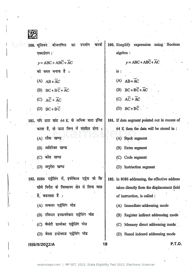
Text of page 21
100.                          ^                 100. Simplify expression using ^ Boolean
                                                       algebra :

       y = ABC+ ABC+ AC                                       _y = ABC+ ABC+AC

             -H^d "^^TFTT "i" :                        is :    .


       (A) AB + AC                                    (A) AB+ AC

       (B) BC+ BC+ AC                                 (B) BC+BC+ AC

       (C) AC + AC                                    (C) AC + AC

       (D) BC+ BC                                     (D) BC+BC


101.^^^ 64 K ^ srto ^ #I?I                        101. If data segment pointed out in excess of

              t, Tit ^ler ^       wflrr #Tr :          64 K then the data will be stored in :


       (A)                                            (A) St^k segment

       (B) 5RjMW                                      (B) Extra segment

       (C)                                            (C) Code segment

       (D) 37^^                                       (D) Instiuction segment


102. 8086                         "q^ # % 102. In 8086 addressing, the effective address
                                                       taken directly from the displacement field
 ■ t, 4i^dld! t :                                      of instruction, is called :

       (A) Tic^qd M.4nH'M ite                         (A) Immediate I addressing mode

       (B)            $4^14^4^^ v^n Tcte              (B) Register indirect addressing mode

       (C) "W ^1^4^               fffe                (C) Memory direct addressing mode

       (D)                        h1^                 (D) Based indexed addressing mode

(5)S/9/2022/A                                19                                           P.T.O.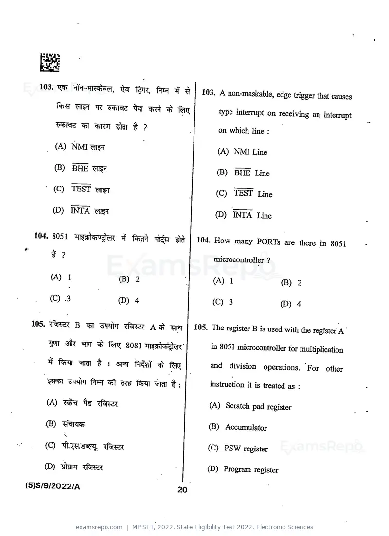
Text of page 22
103.                          %r 1^, f5[CT     ^
                                                        103. A non-maskable, edge trigger that cames
                   WT                     ^ ^ %ii            type interrupt on receiving an interrupt
                   ^ ^JTW ?teT t ?
                                                             on which line :

         (A) NMI
                                                            (A) NMI Line

         (B) BHE ^
                                                            (B) BHE Line

         (C) TEST enn
                                                            (C) TEST Line

        (D) INTA ^                                          (D) INTA Line

  104. 8051                                     ^ 104. How many PORTs are there in 8051
        t ?
                                                            microcontroller ?

        (A) 1                (B) 2                         (A) 1                 (B) 2
        (C) .3               (D) 4                         (C) 3                 (D) 4

 105.              B ^                                105. The register B is used with the register A
        IPIT       ^^              8081                    in 8051 microcontroller for multiplicatioa
                   ^t I                    ^               and division operations. For other
        WT                    ^           ^                instruction it is treated as :

    (A)                  Tf^R^                            (A) Scratch pad register

    (B)                                                   (B) Accumulator
               s


    (C)                   Xpi1W<                         (C) PSW register

    (D) yluiH                                            (D) Program register

(5)S/9/2022/A                                    20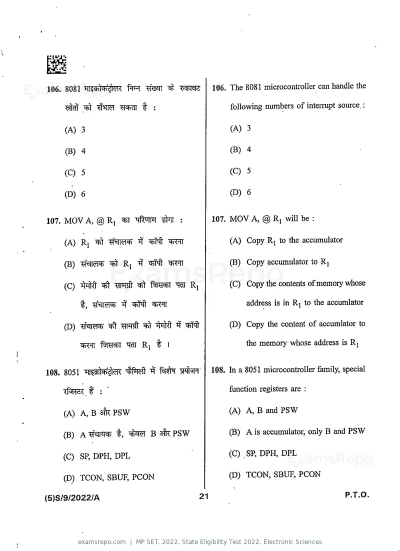
Text of page 23
106. 8081 Hi55hictJdlcn< "f^T^                           106. The 8081 microcontroller can handle the

     ^hif                        "I" :                        following numbers of interrupt source, :

     (A) 3                                                    (A) 3

     (B) 4                                                    (B) 4

     (C) 5                                                    (C) 5

     (D) 6                                                    (D) 6


107. MOV A,@ Rj ^                        #TT :           107. MOV A, @ Rj will be :

    (A) Ri ^                                                  (A) Copy Rj to the accumulator

    (B)            ^ Rj           ^                           (B) Copy accumulator to Rj

    (C)          ^           ^ r^^=bl            Ri          (C) Copy the contents of memory whose

            t,         ■^*                                         address is in Rj to the accumlator

     (D)               "^TTOt ^             "4* ^rfqt        (D) Copy the content of accumlator to

            chiil f^RT^ HOI Rj ^ I                                 the memory whose address is Rj


108. 8051 Hl^s6Wild<                         3Bft^" 108. In a 8051 microcontroller family, special
     Tf^.t :                                                  function registers are :


     (A) A, B 3Tk PSW                                        (A) A, B and PSW

     (B) A ^*^1441 t,              B 3fk PSW                 (B) A is accumulator, only B and PSW

     (C) SP, DPH, DPL                                        (C) SP, DPH, DPL


     (D) TCON, SBUF, PCON                                    (D) TCON, SBUF, PCON

                                                    21                                         P.T.O,
(5)S/9/2022/A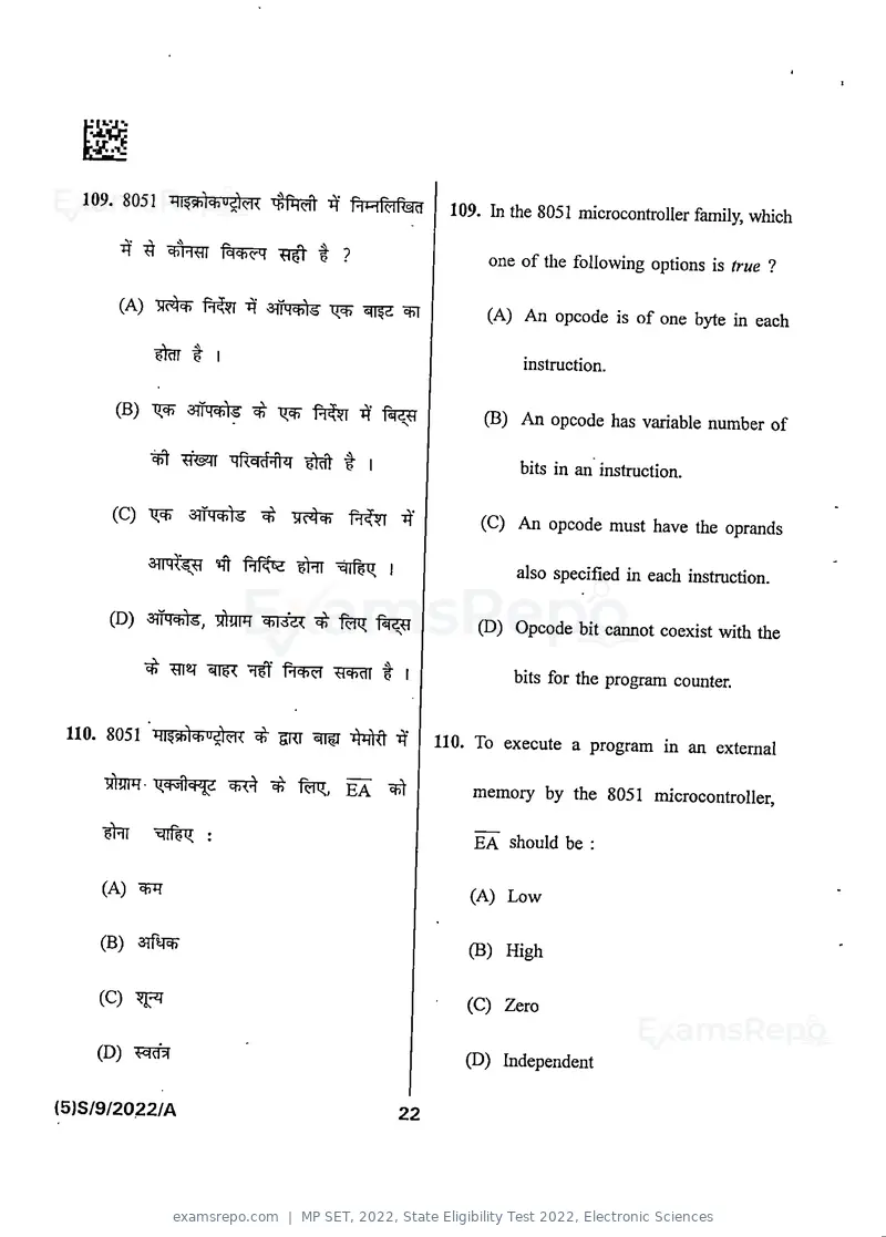
Text of page 24
109. 8051                                   PiHldRsirf
                                                               109. In the 8051 microcontroller family, which
        ■^' ^               f^chrM      t ?                         one of the following options is true ?

       (A)                    ■^' afpT^^ -[T^           ^           (A) An opcode is of one byte in each
               ^tclT t" I
                                                                        instruction.


       (B) TT^ arrq^ ^                          t^*                (B) An opcode has variable number of

              ^              HRcicfnl^i ^ f I                           bits in an instruction.

      (C)             ^Tn^tiU ^ yc^ch"                  "4'        (C) An opcode must have the oprands
                           ^ Rfe #rT ^irf^ I                            also specified in each instruction.

      (D) 3TR^, -ytoFT cbl^idi ^                                   (D) Opcode bit cannot coexist with the

             "^" "^rrsiT       "^i^" -Rt^             t I              bits for the program counter.

 110. 8051 Hl^sblchual^^^ ^ ^ ^                        :^-    110. To execute a program in an external

     3toPT-                          %TT,             ^           memory by the 8051 microcontroller,
     "?Rtt     ■qif^y. :
                                                                  EA should be :


     (A) ^                                                        (A) Low

    (B) 3Tte                                                      (B) High

    (C) ^                                                        (C) Zero

    (D) ^a'pi                                                    (D) Independent

{5)S/9/2022/A                                          22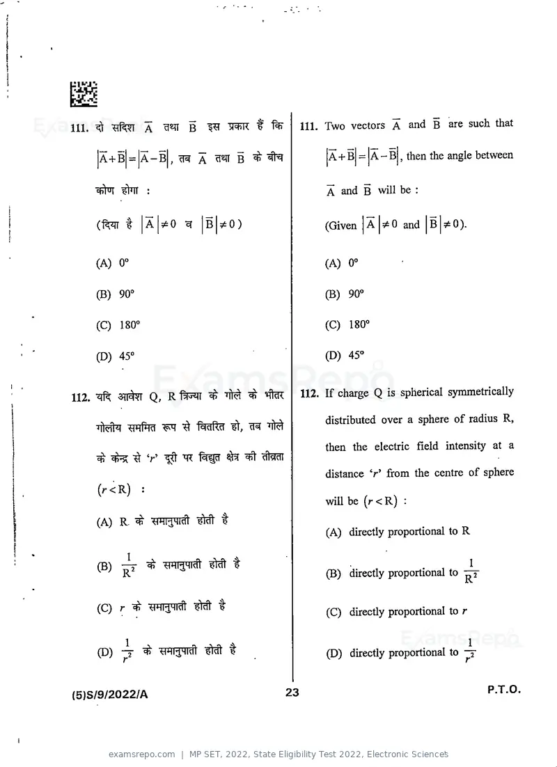
Text of page 25
111. ^        A          B W         f % 111. Two vectors A and B are such that

    A+B       A-B   ,      A       B ^^          A +B     A-B , then the angle between


   ^ #TT :                                       A and B will be :


   (1^ t A ?s:0 ^ B ^iO)                        (Given A ^0 and B 9^0).


   (A) 0°                                       (A) 0°

   (B) 90-^                                     (B) 90°

   (C) 180°                                     (C) 180°

   (D) 45°                                      (D) 45°


112.^ 371^ Q, R 1^r?2TT ^          ^ ^ 112. If charge Q is spherical symmetrically
                                                distributed over a sphere of radius R,
                        ^ l^ciRd    cl^
                                                then the electric field intensity at a

                                                distance V from the centre of sphere
    (.<R) :
                                                will be (/• < R.) :
    (A) R. ^              ^t
                                                (A) directly proportional to R

    (B) ^ ^                 ^t
                                                (B) directly proportional to ^
                                                                                 1


    (C) r ^ ^HI^HIdl ^ t                        (C) directly proportional to r

                                                                                 1
    (D)       ^            ^t                   (D) directly proportional to


                                          23                                         P.T.O.
(5)S/9/2022/A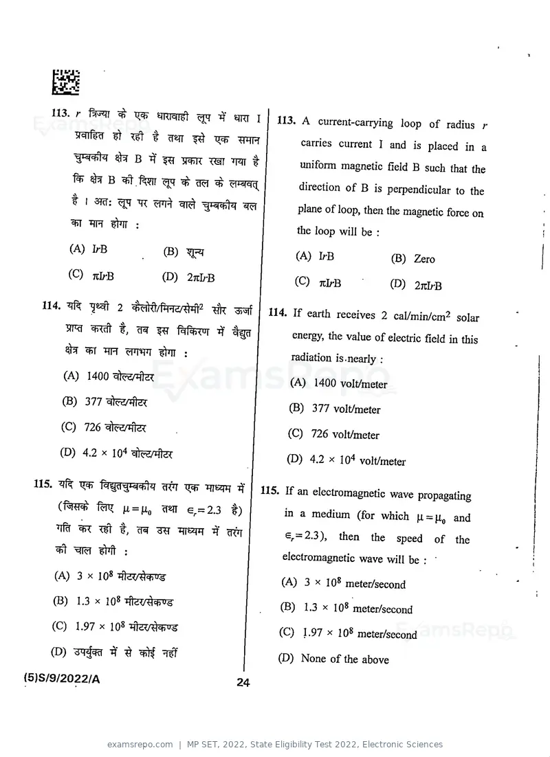
Text of page 26
'r^4

    113. r           ^                 ^      TO I 113. A current-carrying loop of radius r
                                                           carries current I and is placed in a
                    ^B         1^ "STO        TO f         uniform magnetic field B such that the
                ^ B ^ -fen ^^ TO ^                         direction of B is perpendicular to the
           tI        ^ tR to4           ^^itoN To         plane of loop, then the magnetic force on
          ^ TO ^ :
                                                          the loop will be :
          (A) IrB              (B) ^                      (A) IrB                (B) Zero
          (Q KlrB              (D) 2KlrB                 (C) TtlrB               (D) 2jrIrB
   114.         "^8^ 2 ^ell<l/#PIH/#qt2              114. If earth receives 2 cal/min/cm^ solar
          TO! TOft %, -^ -^ Uhiui if
                                                         energy, the value of electric field in this
          ^ ^ TO              ^:                         radiation is-nearly :
        (A) 1400 ^te/rte
                                                        (A) 1400 volt/meter
        (B) 377^WTfe
                                                        (B) 377 volt/meter
        (C) 726
                                                        (C) 726 volt/meter
        (D) 4.2 X io4 -cjloTi/Hld^:
                                                        (D) 4.2 X lo'* volt/meter

 115.       TO l^lcr^TOfhT TO TO "^TO if        115. If an electromagnetic wave propagating
        (i^R#         ^=              e^=2.3 f)      in a medium (for which |i = R(, and
     ^ TO             t, ^ TO tttTO          TO         g^=2.3), then the speed of the
     ^ "TOT           :
                                                       electromagnetic wave will be : "
     (A) 3 X IQS
                                                       (A) 3 X 10^ meter/second
    (B) 1.3 X IQS Tftro^^yrrg-
                                                      (B) 1.3 X iqS meter/second
    (C) 1.97 X IQS -qtro^TO?
                                                      (C) 1.97 X 10^ meter/second
    (D)                ^^                             (D) None of the above

(5)S/9/2022/A                                  24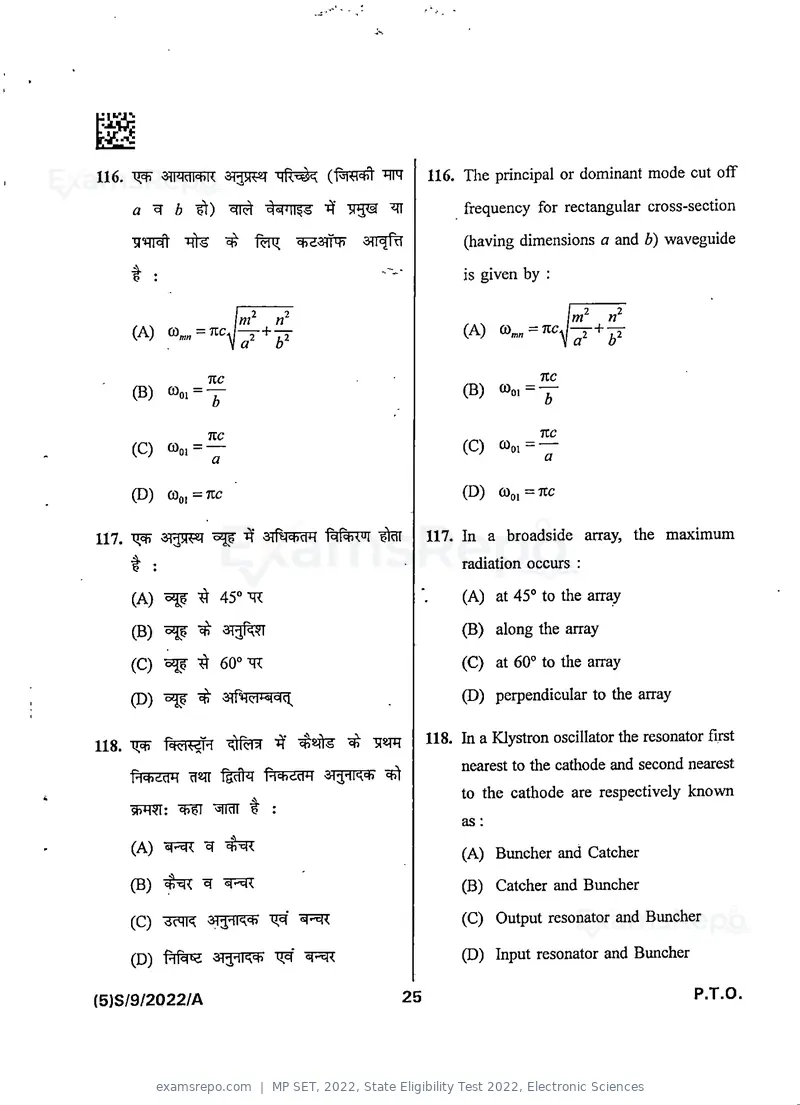
Text of page 27
116.                            mR-^<         ^         116.   The principal or dominant mode cut otF
         ^ A              ^             ■^* ITH^ ^             frequency for rectangular cross-section
                          ^ %TT             3TT^               (having dimensions a and b) waveguide
       t :                                                     is given by :

                        t?                                                           rj'
       (A) co^„ = ncJ^-i-^                                     (A) (0^„ = 'ric^l—+^2
                                                                                 a


                   nc                                                      Tic
       (B) ®oi=y                                               (B) ®oi=y

                   7UC                                                     TtC
       (C) ©0,=                                                (C) ©01 ~
                      a                                                    a


       (D) a)oj=nc                                             (D) ©o,=7CC


117.                ^         aifeclH                   117. In      a broadside array, the maximum
       t :                                                     radiation occurs :

       (A) ^ ^ 45° -qi                                         (A) at 45° to the array

       (B) ^ ^ 373!^                                           (B) along the array

       (C) ^ ^ 60° "qr                                         (C) at 60° to the array

       (D)        "^" 3lfiiQl+^qq^                             (D) perpendicular to the array

                                                        118. In a Klystron oscillator the resonator first
118.         Rkrl^H "qtf^                 ^ "q^R
                                                               nearest to the cathode and second nearest
       PicbddM ^sqr           fe^FT sT^qrqF ^
                                                               to the cathode are respectively known
       ITOT:          "^^nHT t" :
                                                               as:


       (A) ®FF                                                 (A) Buncher and Catcher
       (B)        ^                                            (B) Catcher and Buncher

       (C) "^FK                                                (C) Output resonator and Buncher

       (D) "Rrf^ aq^qrqq?                                      (D) Input resonator and Buncher

(5)S/9/2022/A                                      25                                             P.T.O,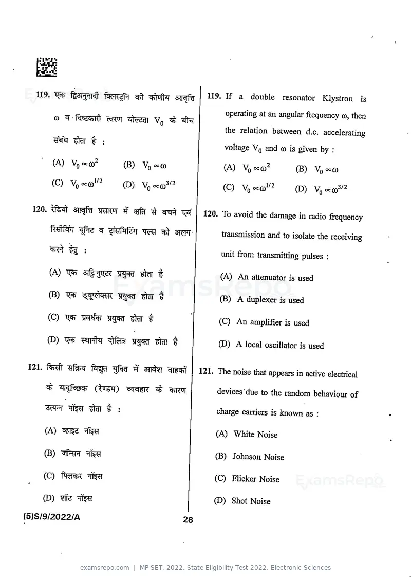
Text of page 28
119.                          qfft 'chluD-M 3TI^ 119. If a double resonator Klystron is
                                                            operating at an angular frequency co, then
          ®^                    cileedl Vq ^
                                                           the relation between d.c. accelerating
              ^t :
                                                           voltage Vq and co is given by :
         (A) VoOcQ)2          (B) Vo«:0)                  (A) Vpocco^           (B) Voocco
         (C) Vq            (D) Vo occo^^^                 (C) Vo°=(b"2          (D) Vqocco^'^
  120.                mm        ^ i{ -w^ m           120. To avoid the damage in radio frequency
         1wif^ \Pid ^ di^rnldJi        ^ 3TOT             transmission and to isolate the receiving
                                                          unit from transmitting pulses :
        (A) TT^           "51^ ^ f                       (A) An attenuator is used

        (B)               "ST^         f                 (B) A duplexer is used

        (C)                     ^t                       (C) An amplifier is used

        (D)             ^1Ri^         ^klT t             (D) A local oscillator is used

 121.         TTfer
                                                    121. The noise that appears in active electrical
        ^             (Wtt)           ^                  devices due to the random behaviour of
              ^^ t :                                     charge carriers is known as :

    (A) °5l^d HT^'U                                     (A) White Noise

    (B) ^TRTT                                           (B) Johnson Noise

    (C) r4^d»<                                          (C) Flicker Noise

    (D) ?1TS                                           (D) Shot Noise

(5)S/9/2022/A                                  26
Text of page 29
122.                                                 CO^
                                                                  122. If 0)„ is the maximum frequency
                                                                       component of the baseband, then the
         ^ AM                 ^ ^■c^'Ji            "Jl-si^
                                                                       transmission bandwidth of AM signal
       i\^ :                                                         • will be:


                                      (®-J                             (A) a                  (B)
                                                                                                    K)
       (A) 0)„                  (B)                                              m


       (C) 2C0,                 (D) 0                                  (C) 2ffl               (D) 0


123. RMfdHsld                                         ^           123. Which of the following is not a
                                                                       characteristic of Photodetector ?
                          t ?
                                                                       (A) High quantum efficiency
       (A) "3^ cWI*<iH
                                                                       (B) Low dark current
       (B) 1^ ^
                                                                       (C) Adequate spectral and frequency
       (C)                   "^3;^* 311^ SI^feT                                response


       (D)                ^ =t>l^ ddl                                  (D) None of the above

124.          f^til M-^iRI              *=tTl< ^                  124. If refractive index of material of core of
                          ' |Xi' W           ^                         optical fiber is ' llj ' and that of clad is
             3TO#Tf^ 'IJ,^'              NA #]T :                      ' [ij    then its NA is :

              (l^i-M-a)
       (A)                                                             (A)


       (B)                                                             (B)


       (C)                                                             (C)


                                                             27                                             P.T.O
(5)S/9/2022/A
Text of page 30
125.             ^
           ■»
                                                   125. Companding is used to :
          ? I
                                                         (A) overcome quantizing noise in PCM
          (A) PCM ^                 -OT^T
          (B) PCM HRFftZT ^ R-t[lc^< if 3TRIP7          (B) allow amplitude limiting in the

                      tR^nkui ^                              receiver of PCM transmitter

     ■ (C) PCM 1^ ^ RjHefT ^                            (C) protect small signals in PCM from

                        ^ lifer ^                            quantization deformation

       (D) PCM feft^ "^f fq^ -qi^                       (D) overcome impulse noise in PCM
                                                            receivers


  126. PIN Wileilsiql^ IRJW ^                     126. PIN Photodiode works as photodetector
                t, ^ ^ ^ t ;                           when connected :

      (A) 37?i arfro                                   (A) Forward biased

      (B) ^ 3#FT^                                      (B) Reverse biased

      (C) ar-^rf^Fm                                   (C) Non-biased
     (D) ^ cit (A) ^ (C)                              (D) Either (A) or (C)

 127. ^            Mi :                          127. Baud rate is :

     (A) eA^fll fe HRPTR ^ ^                          (A) always equal to the bit transfer rate
     (B)           37iq^ "^lei ^        ^            (B) equal to twice the bandwidth of an
                                                          ideal channel

     (C) fe^fer ^ ^                                  (C) not equal to signalling rate
    (D) TTqr 37Tq?f         ^^          ^            (D) equal to one half the bandwidth of
            auMt                                          an ideal channel


(5)S/9/2022/A                               28
Text of page 31
rI   *.


In
                                                128. Satellites     used    for   intercontinental

                                                     communication are known as :


       (A) WT^                                      (A) Comsat


       (B)                                           (B) Domsat


       (C)                                           (C) Marisat


       (D)                                          (D) Intelsat
                                                            «


129. Q-fe^ ^ t :                                129. Q-switch laser is :


       (A)                                           (A) Continuous laser

       (B)           ^                               (B) Short burst laser


       (C) n^F^M "SRT          Pi^Fhi                (C) Laser output by switching

       (D) ^          ^                              (D) Low power laser


130.                     Wg, "f^TR^      'if    130. If 'Xq'        is     the    wavelength    of

             STNicfcT Ti^^fq Tj^n^ ^ OT "dMf         monochromatic light, ^(T is diameter of

       '^q', -^AR-^d 3N^ 'NA'           ^^           core and 'NA'is numerical aperture, then

       3RTm ^ #1 V WIT ^ ^^ :                        V number of this optical fiber will be :

              ndX^                                         TidXr,
       (A)                (B) :^oi/NA                (A)                     (B) X^dNA
               NA          I
                                                            NA

              tu^A                NA                       TtdNA                     NA
       (C)                                           (C) ^                   (D) itdX,


(5)S/9/2022/A                                  29                                           P.T.O,
Text of page 32
131. DIAC ^             ^ ^ ^^ I .
                                                        131. DIAC is also called ;
           (A) fs^^ilq        8?Rf^
                                                             (A) Bidirectional Diode Thyristor
           (B)                   8^pTffel
                                                             (B) Unidirectional Diode Thyristor
        (C)                    siFTffe^
                                                            (C) Multidirectional Diode Thyristor
        (D)         ^gpfe
                                                            (D) Directional Diode Thyristor
   132. "PfRf^ffw ■^'                      TRIAC ^ 132. Which of the following is not a
                     ^ t ?
                                                            characteristic of TRIAC ?
       (A)
                                                           (A) Negative resistance
       (B) ^ efif^
                                                           (B) Five terminals
       (C) -m it.vj\.
                                                           (C) Four P-N junctions
      (D) tgcTTO
                                                          (D) Bilateral conduction

 133. -qm Zff^ ^                               ^
                                                     133. The vertical structure of power transistor
                 ^ ^icil "i", cKil'f^ "q^ .
                                                          is preferred because it :
      (A)           ^ qTq[q Tif^q ^
                                                          (A) increases the thermal resistance of
            t
                                                               transistor

     (B)                 -Srf^sr ^
                                                         (B) decreases the on-state resistance
     (C)           HR-^^             qi^
                                                         (C) decreases the cross-sectional area
                 ^ ^ ^ TO 31^ M t                             through which device current flows
    (D) iroro                  -spqj f
                                                        (D) decreases the breakdown voltage
(5)S/9/2022/A                                   3q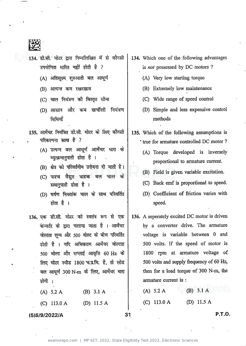
Text of page 33
134.          "Rte OT PHHrdHsId                  134. Which one of the following advantages
       dM^lPldl ^^^ t ?                               is not possessed by DC motors ?

       (A)                                            (A) Very low starting torque

       (B) 37?^ ^                                     (B) Extremely low maintenance

       (C) ^ 1¥m ^                                    (C) Wide range of speed control

       (D) siraH ^ ^ tsNM                             (D) Simple and less expensive control
                                                          methods


135.                        TfR7 ^               135. Which of the following assumptions is
       MRdicrMdl WI t ?                             ^ true for armature controlled DC motor ?

       (A) "3?^ ^                        TO ^         (A) Torque developed is inversely
           oJcTOT^^TTcft     f I
                                                          proportional to armature current.
       (B) ^^ -qfM^ "3^^ ^t I
                                                      (B) Field is given variable excitation.
       (C) HK-q            "TO^         "did ^
           <H^i:iHidl       t I                       (C) Back emf is proportional to speed.

       (D)^ Pdddldi W ^ "^TT^T MRcjPcid               (D) Coefficient of friction varies with
                  t I                                      speed.

136. "P;^ ^."Ht". fta              ^ ^ TT^       136. A seperately excited DC motor is driven
                 ^ TO         ■« t I -311#^           by a converter drive. The armature
       %3dT ^ ak 500 %e ^ ^ MRdRid                    voltage is variable between 0 and
       ^ t I "^if^ 3TfTO?FT 3TT#cR                    500 volts. If the speed of motor is
       500        sfR wrf 3TI^ 60 Hz ^                1800 rpm at armature voltage of
             fte ^ 1800^.3I.1tt. t, ^                 500 volts and supply frequency of 60 Hz,
             37T^ 300 N-m Riy., 37T^^ TOT             then for a load torque of 300 N-m, the
             :                                        armature current is :

       (A) 5.2 A            (B) 3.1 A                 (A) 5.2 A           (B) 3.1 A

       (C) 113.0 A          (D) 11.5 A                (C) 113.0 A         (D) 11.5 A

(5}S/9/2022/A                                 31                                        P.T.O,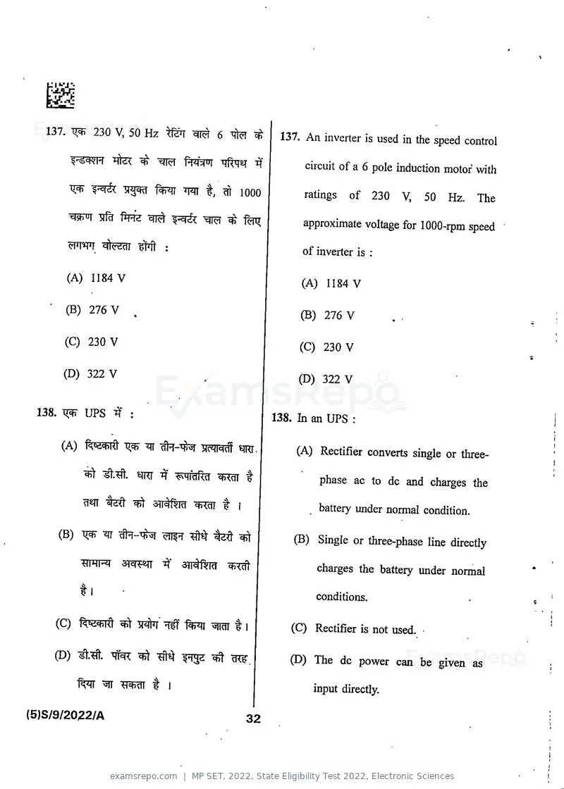
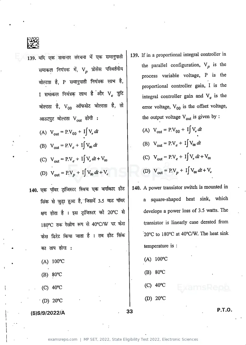
Text of page 35
I


                                                      139. If in a proportional integral controller in
139.       ^
                                                             the parallel configuration, V^ is the
                                                             process variable voltage, P is the
              t, P w^wt                         t,
                                                             proportional controller gain, I is the
       I            PlM^=t)      ^       Vg                  integral controller gain and Vg is the
       c^Wdi i, Vqo                        t, ^              error voltage, Vqq is the offset voltage,
       aiT^Z^S ciWdl Vout            :                       the output voltage Vo^t is given by :

       (A) V„„,= P.Voo+ ijv.t?/                            (A) v„„,= p.Voo+ ijv.rf;    %


       (B) V„„,= P.V,+ lJv<„fif^                             (B) V„„,= P.V,+ljv„„rff
       (C) v„„,= P.v,+ijv,rfr+v„„                            (C) v„„,= p.v,+ijv,rf;+v„„

       (D) v„„t = P.Vp+ ijv„rf;+v,                           (D) V„„,= P.Vp+ ljv„„<//+ v,

140.       "^Tf^ zff^T^           1?^ M^lIchK ^       140.   A power transistor switch is mounted in

            ^         I^IT t,        3.5 ^ w                 a square-shaped heat sink, which

       ^ ^ t I ^ <i\\ki«.                20°C                develops a power loss of 3.5 watts. The

        180°c ^                 ^ 40°C/W      ^              transistor is linearly case derated from

            "fefe               t 1 ^ ^ 1^                   '20°C to 180°C at 40°C/W. The heat sink

       ^ ^ #Tt :                                             temperature is :


       (A) 100°C                                             (A) lOO^C

       (B) 80°C                                              (B) 80°C


  . (C) 40°C                                                 (C) 40°C

       ■ (D) 20°C                                            (D) 20°C

                                                     33                                          P.T.O.
 (5)S/9/2022/A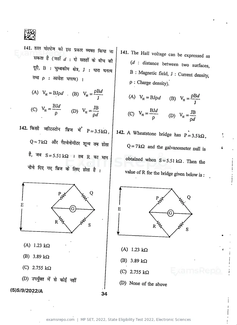
Text of page 37
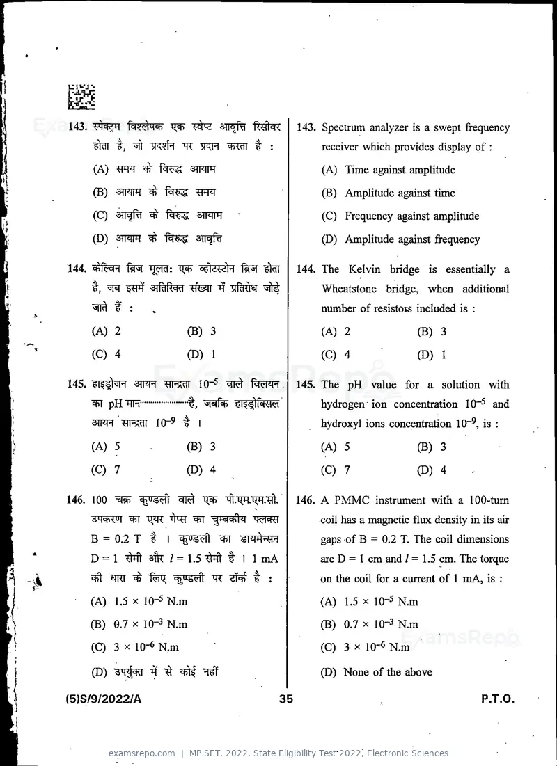
143.                                                        143. Spectrum analyzer is a swept frequency

             "I,     3i^#T          31^ ^RX?n "I :               receiver which provides display of :

       (A)         ^          3MH                               (A) Time against amplitude

       (B) 3WT ^                WT                              (B) Amplitude against time

       (C) 371^ ^               3TFTR                           (C) Frequency against amplitude
       (D) 3Tm ^ 1^^ air#f                                      (D) Amplitude against frequency

144.                "*3^:                        "?kn       144. The   Kelvin bridge is essentially a
       t, ^^ srifer                    -^f -jiM?? ^              Wheatstone bridge, when additional
       "^n^ "f :                                                number of resistors included is :

       (A) 2                 (B) 3                              (A) 2                (B) 3
       (C) 4                 (D) 1                              (C) 4                (D) 1

145.               aim Trrmr 10-^ ^ 1^em                    145. The   pH value for a solution with
          pHm*               'f",          5i^'§l[^Qri          hydrogen ion concentration 10"^ and
       aim'^^Timr 10"^ t I                                      hydroxyl ions concentration 10"^, is :
       (A) 5                 (B) 3                              (A) 5                (B) 3

       (C) 7                 (P) 4                              (C) 7                (D) 4        .

146. 100 mi 4iu^dl ^ 13;^ it.'qB.'QTT.'^Tt. ■               146. A PMMC instrument with a 100-turn
       aM4iiui m              ^ -^^4)14 "fimiT                  coil has a magnetic flux density in its air
       B = 0.2 T t I                   ^                        gaps of B = 0.2 T. The coil dimensions
       D=1 M3ffT/=1.5^t I 1mA                                   are D = 1 cm and / = 1.5 cm. The torque
       ^ mr         1^ 4i"-seil "41            "I" :            on the coil for a current of 1 mA, is :

       (A) 1.5 X 10⁻⁵ N.m                                       (A) 1,5 X 10⁻⁵ N.m
    (B) 0.7 X 10⁻³ N.m                                          (B) 0.7 X 10⁻³ N.m
       (C) 3 X 10-^ N.m                                         (C) 3 X 10⁻⁶ N.m

       (D)             ^^                                       (D) None of the above

(5)S/9/2022/A                                          35                                             P.T.O.
Text of page 39
m

                  (SPACE FOR ROUGH WORK)


}•


     S/9/2022/A
             ft
Text of page 40
TV <*>|4   leTtT

             (SPACE FOR ROUGH WORK)


S/9/2022/A
Text of page 2
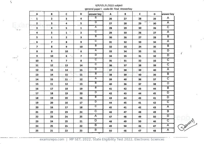
R/P/P/S /II/2022 subject
                       -general paper I -code-00 Final Answerkey
 A    B    C      D       answer key        A              B       C    D    inswer key
                                B.                                               A
 1    2    3      4                         26             27      28   29
                                D                                                A
 2    3    4      5                         27             28      29   30
                                A                                                C
 3    4    5      1                         28             29      30   26

                                C                                                A
 4    5    1'     2                         29             30      26   27

                                B                                                B
 5    1    2      3                         30             26      27   28

                                C                                                A
. 6   7    8      9                         31             32      33   34

                                B                                                B
 7    8    9      10                        32             33      34   35

                                A                                                D
 8    9    10     6                         33             34      35   31
                                D                                                D
 9    10   6      7                         34             35      31   32

                                C                                                C
 10   6    7      8                         35             31      32   33
                                C                                                C
 11   12   13     14                        36             37      38   39

                                D                                                A
 12   13   14     15                        37             38      39   40

                                B                                                B
 13   14   15     11                        38             39      40   36

                                A                                                C
 14   15   11 -   12                        39             40      36   37

                                B                                                D
 15   11   12     13                        40             36      37   38
                                B                                                B
 16   17   18     19                        41             42      43   44

                                D                                                D
 17   18   19     20                        42             43      44   45

                                B                                                D
 18   19   20     16                        43             44      45   41
                                D                                                C
 19   20   16     17                        44             45      41   42

                               C                                                 A
 20   16   17     18                        45             41      42   43

 21   22   23     24           C            46             47      48   49       B

 22   23   24     25           A            47             48      49   50       D

 23   24   25     21           D            48             49      50   46       C

 24   25   21     22           B            49             50      46   47       A

 25   21   22     23           B            50             46      47   48       A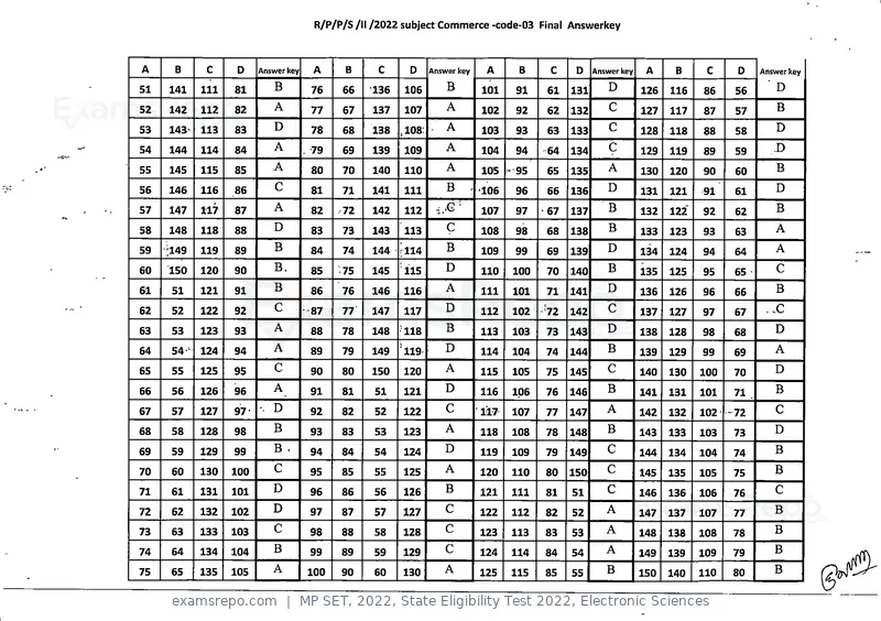
Text of page 3
R/P/P/S/II/2022 subject Commerce-code-03 Final Answerkey


A     B      C     D    Answer key     A    B     C       D    Answer key     A      B     C     D    Answer key    A     B      C     D    Answer key

51   141    111   81       B          76    66   ■136   106         B        101     91    61   131      D         126   116    86     56      D

52   142    112   82       A          77    67   137    107         A        102     92    62   132      C         127   117    87     57      B

53   143-   113   83       D          78    68   138    ,108: -     A        103     93    63   133      C         128   118    88     58      D

54   144    114   84       A         . 79   69   139    109         A        104     94    64   134      c         129   119    89     59      D

55   145    115   85       A          80    70   140    110         A        105    '95    65   135      A         130   120    90             B
                                                                                                                                       60

56   146    116   86       C          81    71   141    111        B        - 106    96    66   136      D         131   121    91     61      D

57   147    117   87       A          82    72   142    112       -h'G'      107     97   ■67   137      B         132   122"   92     62      B

58   148    118   88       D          83    73   143    113         C        108     98   68    138      B         133          93             A
                                                                                                                         123           63

59   :149   119   89       B          84    74   144    rll4       B         109     99   69    139      D         134   124    94     64      A

60   150    120   90       B.         85    75   145    115        D         110    100   70    140      B         135                         C
                                                                                                                         125    95     65

61    51    121   91       B          86    76   146    116         A        111    101   71    141      D         136   126                   B
                                                                                                                                96     66

62    52    122   92       C          87    77   147    117        D         112    102   72    142      C         137   127    97     67

63    53    123   93       A          88    78   148    -118       B         113    103   73    143      D         138                         D
                                                                                                                         128    98     68

64    54'   124   94       A          89    79   149    'll9       D         114    104   74    144      B         139   129    99             A
                                                                                                                                       69

65    55    125   95       C          90    80   150    120        A         115    105   75    145      C         140   130    100    70      D

66    56    126   96       A          91    81    51    121        D         116    106   76    146      B         141   131    101            B
                                                                                                                                       71

67    57    127   97*      D          92    82    52    122        C         117    107   77    147      A         142   132    102            C
                                                                                                                                      -72

68    58    128   98       B          93    83    53    123        A         118    108   78    148      B         143   133    103    73      D

69    59    129   99       B .        94    84    54    124        D         119    109   79    149      C         144   134                   B
                                                                                                                                104   74

70    60    130   100      C          95    85    55    125        A         120    110   80    150      C         145   135    105   75       B

71    61    131   101      D          96    86    56    126        B         121    111   81    51       C         146   136    106   76       C

72    62    132   102      D          97    87    57    127        C         122    112   82    52       A         147   137    107   77       B

73    63    133   103      C          98    88    58    128        C         123    113   83    53       A         148   138    108   78       B

74    64    134   104      B          99    89    59    129        C         124    114   84    54       A         149   139    109   79       B

75    65    135   105      A         100    90    60    130        A         125    115   85    55       B         150   140    110   80       B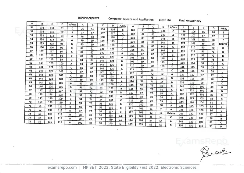
Text of page 4
R/P/P/S/II/2022   Computer Science and Application CODE 04      Final Answer Key


                                                       Delete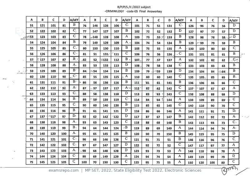
Text of page 6
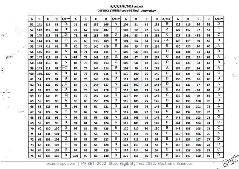
R/P/P/S /II /2022 subject
                                                    -DEFENCE STUDIES-code-06 Final Answerkey


A     B      C     D     A/KEY     A       B       C      D     A/KEY       A        B      C      D    A/KEY      A      B          C       D    A/KEY

51    141   111    81     D.      76       66     136    106       A       101       91     61    131       B-    126    116        86      56      D

52    142   112    82     D-      77       67     137    107       Q       102       92     62    132       A     127    117        87      57      G

53    143   113    83             78       68     138    108       D       103 !- • "93     63    133       G     128    118; > 88          58      C

54.   144   114    84     O       79       69     139-   109       B       104       94     64    134 . -A        129    119        89      59      D

55    145   115    85     B-      80       70,.   140    110       B       105       95     65    135       B,    130    120        90      60    „--A
                          A                                        C                                        D                                       D
56    146   116    86             81.. V   71     141    111               106       96    rc66   136             131    121        91     -.61

57    147   117    87     A                72     142    112,      D.      107      .;97    67    137       G     132    122        92/-    62      A

58-   148   118    88     A       83       73     143    113       C       108       98     68    138       D    . 133   123        93      63      B

59    149   119    89:            84       74     144    114       B-     - ;109     99     69    139       A     134    ;124       94      64      A

60    150, -120    9b    ^ B      85       75     "145   115       D ■'    110 '    100     70    140       C     135    125        95      65      G

61    51    121•   91     B       86       76     146    116      P        111      101     71    141       D     136    126        96      66      D

62    *52   122    92             87       77     147    117     ^ A       112      102     72    142 ' -   D     137    127        97      67      A

63    53    123    93    ■ D,     88       78     148    118       G       113      103     73    143       B     138    128        98      68      D

64    54    124    94    -Q-      89       79     149    119      D        114     . 104    74    144       C     139    129    ^   99      69      B

65    55    125    95     A       90       80     150    120      D        115      105     75    145       D     140    130        100     70      D

66    56    126    96     B      . 91      81      51    121      D        116      106     76    146       B     141    131        101     71      A

67    57    127    97     O       92       82      52    122       A       117      107     77    147       G     142    132        102     72      A

68    58    128    98     A       93       83      53    123       A       118      108     78    148       A     143    133        103     73      C

69    59    129    99     B       94       84      54    124       A       119      109     79    149       B     144    134        104     74      G

70    60    130    100    D       95       85      55    125       B       120      110     80    150       B     145    135        105     75      C

71    61    131    101    B       96       86      56    126       A       121      111     81    51        D     146    136        106     76      A

72    62    132    102    D       97       87      57    127       B       122      112     82    52        B     147    137        107     77     D

73    63    133    103    C.      98       88      58    128       B       123      113     83    53        C     148    138        108     78     D

74    64    134    104    D      . 99      89      59    129.      A       124      114     84    54        C     149    139        109     79      C,

75    65    135    105    B      100       90      60    130       B       125      115     85    55        B     150    140        110     80     D


                                  00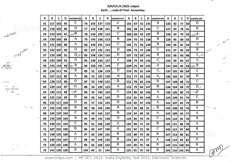
Text of page 7
R/P/P/S /II/2022 subject
                                                         Earth ....-code-07 Final Answerkey


  A      B   C     D      ANSWER KEY       A      B     C     D    ANSWER KEY    A      B     C      D    ANSWER KEY    A     B    C    D     ANSWER KEY


 51     117 102   85         c             76    142   127   110         ■C     101     67   52     135       B        126   92    77   60        D

 52     118 103   86         D             77    143   128   111          B     102     68   53     136       C        127   93    78   61        D

 53     119 104   87.                      78    144   129   112          C     103. :.69    54     137       B'       128   94    79   62    ...rA-
.,54'   120 105   88          A            79    145   130. 113           B     104     70   55     138       B        129   95    80   63        D

 55     121 106   89         A             80    146   131   114          C     105     71   56     139       B-       130   96    81   64        A

 56     122 107   90         D             81'^ 147    132   115         D      106     72   57     140       C        131   97    82   65        B.
                                       I                                                       .1
 57     123 108   91.                      82    148   133   116    .P .        107     73- "58     141      B         132   98    83. 66

 58     124 109   92         D             83    149   134   117          C     108     74   59     142       C,       133   99    84   67        A

 59     125 110   :93t^      B.            84    150   135   118          C     .109-   75   60     143       A        134 100     85   6S

 60     126 111   94         B             85    51    136   119   ... D        ilo     76   61 144                    135   101   86   69      - C

 61     127 112   95         A             86    52    137   120    ■     A-    111     77   62     145                136 102     87   70        D

'62     128 113   96         D'            87    53    138' '121        .-■B    112     78   63     146      D         137 103     88   71:       C

 63     129 114   97'                      88    54    139   122          A     li3     79   '64    147      B>        138   104   89   72       •a;.
 64     130 115   98       '■^rA           89    55    140   123          C     114- 80      65     148       A        139 105     90   73

 65     131 116   99         D             90    56    141   124         D      115     81   66     149      A         140   106   91   74        c

 66     132 117 100          D             91    57    142   125         D      116     82   67     150       A,       141 107     92   75        B

 67     133 118 101          B             92'   58    143   126         B      117     83   68     51       B.        142 108     93   76        A

 68     134 119   102        C             93    59    144   127          B-    118     84   69     52       A         143   109   94   77        A

 69     135 120 103          B             94    60    145   128         D-     119     85   70     53       c ..      144 110     95   78        B.

 70     136 121 104          C             95    61    146   129          A     120     86   71     54       B         145   111   96   79        A

 71     137 122 105          D             96    62    147   130          C     121     87   72     55       C         146 112     97   80        B

 72     138 123   106        A             97    63    148   131         B      122     88   73     56       B         147 113     98   81        A

 73     139 124 107          C             98    64    149   132         B .    123     89   74     57       A         148 114     99   82        D

 74     140 125   108        A ,           99.   65    150   133         D      124     90   75     58       B         149   115 100 83           B

 75     141 126 109          D         100       66    51    134          A     125     91   76     59       B         150 116 101 84             A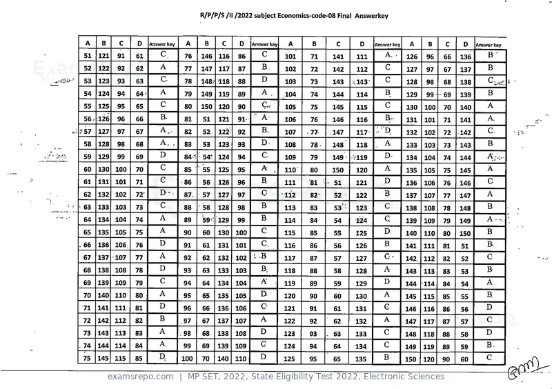
Text of page 8
R/P/P/S /]]12022 subject Economics-code-08 Final Answerkey
A B C D Answer key A B C D Answer key A B C D Answer key A B C D Answer key
51 121 91 61 c. 76 146 116 86 c 101 71 141 111 A. . 126 96 66 136 B'
52 122 92 62 A 77 147 117 87 B, 102 72 142 112 C 127 97 B
67 137
53 123 93 63 C- 78 148.i 118 88 D 103 73 143 ;.113- C 128 98 68 138
54 124 94 64' A 79 149 119 89 A. 104 74 144 114 B 129 99- - 69 139 B
55 125 95 65 C 80 150 120 90 c..- 105 75 145 115 C 130 A
100 70 140
56.:126 96 66 B. 81 51 121 91 A' 106 76 146 B.^- A.
116 131 101 71 141
127 97 67 A... 82 52 122 92 B, 107 -77 .147 117 : 132 102 72 142 C.
58 128 98 68 A, , 83 53 123 93 D- 108 78 148 118 A 133 103 73 143 B
D c. D.
59 129 99 69 ■ 54r. 124 94 109 79 149- V119 134 104 74 144 Ar-v-
60 130 100 70 C 85 55 125 95 A 110' 80 150 120 A 135 A
105 75 145
61 131 101 71 e 86 56 126 96 B, 111 81 • 51 121 D 0
136 106 76 146
62 132 102 72 D-. 87. 57 127 97 C ■112 82 52 122 B A
137 107 77 147
<.
63 133 103 73 c 88 58 128 98 B 113 83 53 123 C 138 108 78 148 B
64 134 104 74 A 89 39 129 99 B 114 84 54 1^4 C A-..
139 109 79 149
65 135 105 75 A 90 60 130 100 C 115 85 55 D. B
125 140 110 80 150
. 66 136 106. 76 D 91 61 131 101 C. 116 86 56 126 B B.
141 111 81 51
67 137 107 77 A 92 62 132 102 I .B 117 C- C
87 57 127 142. 112 82 52
68 138 108 78 D 93 63 133 103 B. 118 88 58 128 A 143 113 83 53 B
69 139 109 79 C 94 64 134 104 A . 119 89 59 129 D A
144 114 84 54
70 140 110 80 A 95 65 135 105 D. 120 90 60 130 A B
145 115 85 55
71 141 111 81 D 96 66 136 106 c- 121 91 61 131 G D
146 116 86 56
72 142 112 82 B 97 67 137 107 A 122 92 62 A C
132 147 117 87 57
73 143 113 83 A 68 138 108 D 123 93 . 63 133 C D
148 118 88 58
- 74 144 114 84 A. 99 69 139 109 G 124 94 64 134 c B.
149 119 89 59
75 145 115 85 D, 100 70 140 110 D 125 95 65 135 B C
150 120 90 60
00
OG
Text of page 9
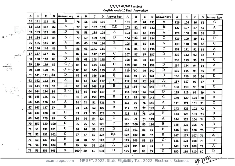
R/P/P/S/l1/2022         Electronic Science       CODE 09           Final Answer Key
A     B      C     D    A/Key    A        B      C         D    A/Key     A          B     C        D      A/Key    A          B     C     D     A/Key
51   131    111   91     B      76        56    136       116     C      101     81       61       141       B     126        106    86   66      B
52   132    112   92     D      77       57     137       117     C      102     82       62       142       C     127        107    87   67      B
53   133    113   93     A      78        58    138       118     D      103     83       63       143       A     128        108    88   68      D
54   134    114   94     C      79        59    139       119     C      104     84       64       144 •     D     129        109    89   69      B
55   135    115   95     C      80       60     140       120     D      105     85       65       145       A     130        110    90   70 ■    C
56   136    116   96     D      81       61     141       121     B      106     86       66       146       C     131        111   91    71      A
57   137    117   97     A      82       62     142       122     A      107     87       67       147       C     132        112   92    72      B
58   138    118   98     C      83       63     143       123     A      108     88       68       148     A,C,D   133        113   93    73      B
59   139    119   99     A      84       64     144       124     C      109     89       69       149       A     134    114       94    74      A
60   140    120   100    C      85       65     145       125     D      110     90       70       150       A     135    115       95    75      C
61   141    121   101    B      86       66     146       126     B      111     91       71       51        B     136    116       96    76      C
62   142    122   102    B      87       67    ■ 147      127     A      112     92       72       52        C     137    117       97.   77      C
63   143    123   103    D      88       68     148       128     D      113     93       73       53        B     138    118       98    78      A
64   144    124   104    A      89       69     149       129     A     114      94       74       54        C     139    119       99    79      C
65   145    125   105    C      90       70     150       130     B     115      95       75       55        c     140    120       100   80      c
66   146    126   106    B      91       71     51        131     D     116      96       76       56        B     141    121       101   81      c
67   147    127   107    B      92       72     52        132     C     117      97       77       57        D     142    122       102   82      c
68   148    128   108    B      93       73     53        133     A     118      98       78       58        A     143    123       103   83      D
69   149    129   109    B      94       74     54        134     D     119      99       79       59        A     144    124       104   84      A
70   150    130   110    A      95       75     55        135     B     120     100       80       60        B     145    125       105   85      A
71   51     131   111    B      96       76     56        136     D     121     101       81       61       D      146    126       106   86      C
72   52     132   112    A      97       77     57        137     C     122     102       82       62       C      147    127       107   87      B
73   53     133   113    D      98       78     58        138     C     123     103       83       63       D      148    128       108   88      D
74   54 .   134   114    B      99       79     59        139     D     124     104       84       64       C      149    129       109   89     D
75   55     135   115    0      100 1    80     60        140     A     125     105       85       65       C      150    130       110   90      B
Text of page 10
R/P/P/S /II/2022 subject
-English -code-10 Final Answerkey
A B C D Answer key A B C D Answer key A B C D Answer key A B C D Answer key
51 131 111 81 B 76 56 136 106 D A C
101 81 - 61 131 126 106 86 56
52 132 112 82 A 77 57 137 107 C,D B A
102 82 62 132 127 107 87 57
53 133 113 83 D 58 138 108 A A B
78 103 83 . 63 133 128 108 88 58
54 134 114 84 A i-~ 79 59 139 109 D 104 "84 C D
64 134 129 109 89 59
55 135 115 85 A 80 60 140 110 B A C
105 85 65 135 130 110 '90 60
.56 136 116 86 B 81 61 -.141 111 B C A
106 86 66 136 131 111 91 61
57 137 117 87 A 82 . 62 142 112 C D C
107 87 67 137 132 112 92 62
58 138 118 88 D. 83 63 143 113 C 108 88' 68 138 C 133 113 93 C
63
59 139 119 89 C 84 64 144 114 c 109 -:89 69 139 D A
134 114 94 64
60 140 120 90 ' 85 65 145 115 A lib "9b 70 D B
140 135 115 95 65
61 141 121 -91 D 86 66 146 116 ?■ D D
111 91 71 141 136 116 96 66
62 142 122 92 A c A
87 67 147 117 112 92 72 142 137 117 97 67 C
63 143 123 93 B. 88 68 148 118 B 113 D C
-93 73 143 138 118 98 68
64 144 124 94 B ' 89 69 149 119 A D A
114 ^:;94 - 74 144 139 119 99 69
65 145 125 95 B 90 70 150 120 B C D
115 95 75 145 140 120 100 70
66 146 126 96 A 91 71 51 121 A A C
116 96 76 146 141 121 101 71
147 B B A
67 127 97 92 72 .52 122 117 97 77 147 142 122 102 72 A
)
68 148 128 98 D 93 73 53 123 A B B
118 98 78 148 143 123 103 73
69 149 129 99 C 94 74 54 124 C A D
119 . 99 79 149 144 124 104 74
70 150 130 100 D 95 75 55 125 C B B
120 100 80 150 145 125 105 75
71 51 131 101 C 96 76 56 126 D B C
121 101 81 51 146 126 106 76
72 C B,D B
52 132 102 97 77 57 127 122 102 82 52 147 127 107 77 A,
73 53 133 103 B 98 78 58 128 B C B
123 103 83 53 148 128 108 78
74 54 134 104 B 99 79 59 129 A C A
124 104 84 54 149 129 109 79
75 55 135 105 A 100 - 80 60 130 D D D
125 105 85 55 150 130 110 80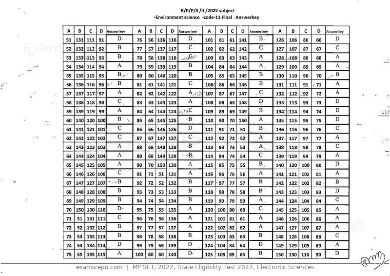
Text of page 11
R/P/P/S /II/2022 subject
                                                  -Environment science -code-11 Final Answerkey


 A     B    C    D    Answer key        A     B     C    D     Answer key    A      B    C    D     Answer key    A     B      C      D    Answer key

51    131 111    91        D.           76    56 136 116            D.      101    81    61   141        B.      126   106    86     66         D

52    132 112    92        B            77    57 137 117            C       102    82    62   142        C       127   107    87     67         C

53    133 ill3   93        B            78    58 138 118                    103    83    63 143          A       128.;108-    88     68         A

54    134 114    94        A            79    59 139 119            B       104    84    64   144        A       129   109    89     69         A       ...

55    135 115    95        B...         80    60 140 120            B       105    85 "65     145        B       130   110    90     70         B

56    136 116    96        B            81    61   141 121          C       106^   86    66   146        B       131   111    91    ; 71        A

.57   137 117. 97          A            82    62 142 122                    107    87    67   147      ,C        132   112:.92       72         A

58    138 118 .98          C            83    63   143 123          A       108    88    68   148        D .     133   113    93     73         D

59.i i39 119 99            A            84    64 144 124                    109    89    69   149        B       134; iM14    94     74         D

60    140 120 100          B       ..   85    65   145 125        -B        110    90    70   150        A       135" 115     95     75         D

61    141 121 101          C            86    66 146 126            D       111    91    71   51         B       136   116    96     76         C

62. 142 122 102            C            87    67 147 127            C       112    92    72   52         A       137. 117     97     77         A

63    143 123 103          A            88    68 148 128            B..     113    93    73   53         A       138   118-   98     78         C

64    144 >124 104         A            89    69   149   129                114    94    74   54         C       139   119    99     79         A

65    145 125 105          A            90    70 150 130            A       115    95    75   55         B,      140   120    100    80         D

66    146 126 106          C            91    71   51    131        A       116    96    76   56        A        141   121    101    81         A

67    147 127 107 - . ..B               92    72   52    132        B       117''97      77   57         B       142   122    102    82         B

68    148 128 108          B            93    73   53    133        B       118    98    78   58        B        143   123    103    83         D       .

69    149 129 109          B            94    74   54    134        B       119    99    79   59        A_       144   124    104    84         C

70    150 130 110          D-           95    75   55    135        A       120    100 80     60        C        145   125    105    85         A

71    51   131 111         C            96    76   56    136        A       121    101 81     61        A        146   126    106    86         A

72    52   132 112         B            97    77   57    137        A       122    102 82     62        A        147   127    107    87         A

73    53   133 113         B            98    78   58    138        B       123    103 83     63        B        148   128    108    88         C

74    54   134- 114        D            99    79   59    139       D        124    104 84     64        D        149   129    109    89         A

75    55   135 115         A            100   80   60    140        D-      125    105   85   65        B        150   130    110    90         D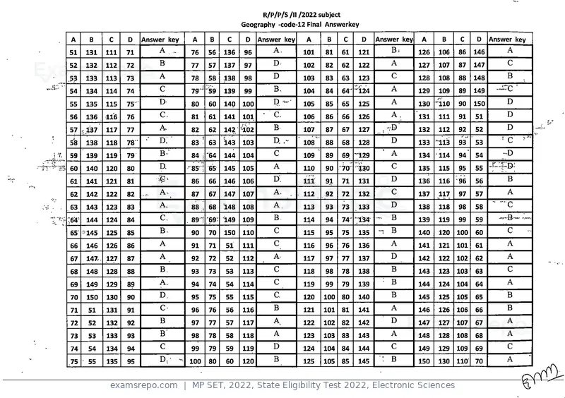
Text of page 12
R/P/P/S/ll /2022 subject
                                                              Geography -code-12 Final Answerkey

 A    B     C     D    Answer key         A        B     C     D    Answer key    A      B    C       D    Answer key   A      B      C    D     Answer key
51    131   111   71         A ..        76        56   136   96        A.       101    81    61     121         B.     126   106    86    146       A

52    132   112   72         B           77        57   137   97        D-       102    82    62     122         A      127   107    87    147       C

.53   133   113   73         A            78       58   138   98        D        103    83    63     123         C      128   108    88    148       B

54    134   114   74         C           79'"59         139   99        B.       104    84    64*   "i24         A      129   109    89    149    --rc '

55    135   115   75         D           80        60   140   100
                                                                        D    '   105    85    65     125         A      130 "110     90    150       D

56    136   116   76         C.          81        61   141   101   ' C-         106    86    66     126         A.     131   111    91    51        D

57          117   77         A           82        62   142   102       B        107    87    67     127    ,tD         132   112    92    52        D
 i                                             1
58    138   118   78    ''   d:'         83        63   143   103       D        108    88    68     128         D      133   -iii   93    53       ■ C    ■

59    139   119   79                     84 ; *64       144   104       C        109    89    69 "^129     ' A          134   114    94    54       -D

60    140   120   80         D.          "85P 65        145   105       A        110    90    70^    130         C      135   115    95    55

61    141   121   81                     86        66   146   106       D.       111'   91    71     131         D      136   116    96    56        B

62    142   122   82                     87        67   147   107       A.       112    92    72     132         C      137   117    97    57        A

63    143   123   83         A.          88 , 68        148   108       A,       113    93    73     133         D      138   118    98    58        C

:64' 144    124   84         C.          89 7 "69^ 149        109       B        114    94    74^ -134           B      139   119    99    59

65 -145     125   85         B.          90        70   150   110       C        115    95    75     135   --r   B      140   120    100   60        C

66    146   126   86         A           91        71   51    111       C        116    96    76     136         A      141   121    101   61        A

67    147-. 127   87         A           92        72   52    112       A-       117    97    77     137         D      142   122    102   62        A

68    148   128   88         B.          93        73   53    113       C        118    98    78     138         B      143   123    103   63        C

69    149   129   89         A.          94        74   54    114       C        119    99    79     139     ■   B      144   124    104   64        A

70    150   130   90         D           95        75   55    115       C.       120    100   80     140         B      145   125    105   65        B

71    51    131   91         C-          96        76   56    116       B        121    101   81     141         A      146   126    106   66        B

72    52    132   92         B           97        77   57    117       A.       122    102   82     142         D      147   127    107   67        A

73    53    133   93         B'          98        78   58    118       A        123    103   83     143         A      148   128    108   68        A

74    54    134   94         C           99        79   59    119       D        124    104   84     144         C      149   129    109   69        C

75    55    135   95         Dp     -■   100       80   60    120       B        125    105   85     145    :    B      150   130    110   70        A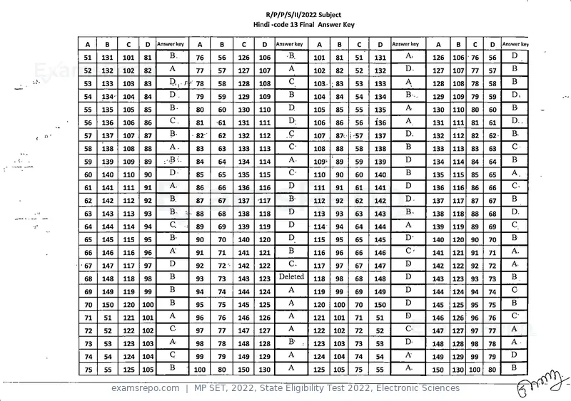
Text of page 13
R/P/P/S/ll/2022 Subject
                                                       Hindi -code 13 Final Answer Key


A     B      C    D     Answer key     A    B     C      D    Answer key    A       B    C     D    Answer key    A     B    C    D    Answer key


51   131    101   81        B.        76    56   126    106      ■B.       101     81    51   131        A,      126   106   76   56      D

52   132    102   82        A         77    57   127    107       A        102     82    52   132       D.       127   107   77   57      B

53   133    103   83        P.,P ' 78       58   128    108       C        103    ; 83   53   133        A
                                                                                                          *      128   108   78   58      B

54   134-   104   84        D.        79    59   129    109       B        104     84    54   134       B        129   109   79   59      D,

55   135    105   85        B-        80    60   130    110       D.       105     85    55   135        A       130   110   80   60      B.

56   136    106   86        C.        81    61   131    111       D:       106     86    56   136        A       131   111   81   61      D.,

57   137    107   87        B-        82    62   132    112       c        107     87c i 57   137       D.       132   112   82   62      B.

58   138    108   88        A.        83    63   133    113       c-       108     88    58   138       B        133   113   83   63      C

59   139    109   89                  84    64   134    114       A-       109-    89    59   139       D        134   114   84   64      B

60   140    110   90        D-        85    65   135    115       C-       110     90    60   140       B        135   115   85   65      A.

61   141    111   91        A.        86    66   136    116       D        111     91    61   141       D        136   116   86   66      c.

62   142    112   92        B.        87    67   137    117       B        112     92    62   142       D-       137   117   87   67      B

63   143    113   93        B-       ^ 88   68   138    118       D        113     93    63   143       B.       138   118   88   68      D.

64   144    114   94        Q .       89    69   139    119       D        114     94    64   144        A       139   119   89   69      C

65   145    115   95        B-        90    70   140    120       D        115     95    65   145       D-       140   120   90   70      B

66   146    116   96        A         91    71   141    121       B        116     96    66   146        C'      141   121   91   71      A.

67   147    117   97        D         92    72   142    122       C-       117     97    67   147       D        142   122   92   72      A

68   148    118   98        B         93    73   143    123   Deleted      118     98    68   148       D        143   123   93   73      B.

69   149    119   99        B         94    74   144    124       A        119     99    69   149       D        144   124   94   74      G

70   150    120   100       B         95    75   145    125       A        120    100    70   150       D        145   125   95   75      B

71   51     121   101       A         96    76   146    126       A        121    101    71   51        D        146   126   96   76      c-

72   52     122   102       C         97    77   147    127       A        122    102    72   52        C        147   127   97   77      A

73   53     123   103       A         98    78   148    128       B' .     123    103    73   53        D-       148   128   98   78      A ■

74   54     124   104       C         99    79   149    129       A        124    104    74   54         A       149   129   99   79      D

75   55     125   105       B        100    SO   150    130       A        125    105    75   55         A.      150   130 100    80      B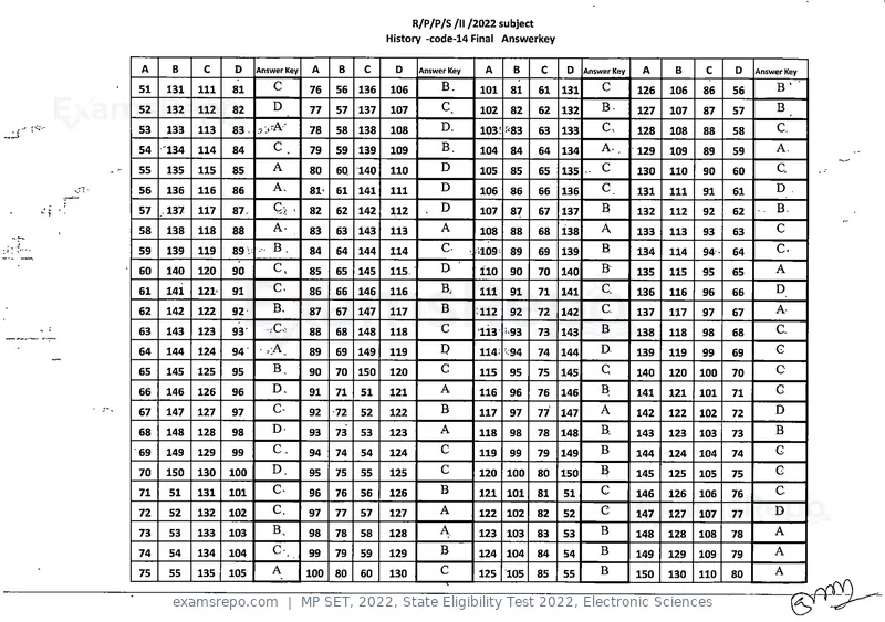
Text of page 14
R/P/P/S /II /2022 subject
                                                       History -code-14 Final Answerkey


A     B      C     D     Answer Key    A    B     C     D      Answer Key    A       B    C     D    Answer Key    A     B     C    D    Answer Key

51   131    111   81        c         76    56   136   106          B.      101     81    61   131       c        126   106   86    56        B' ■

52   132    112   82        D         77    57   137   107          C.      102     82    62   132       B-       127   107   87    57        B

53   133    113   83^                 78    58   138   108          D.      103:          63   133       C,       128   108   88    58        C,

54   "134   114   84        C,        79    59   139   109          B,      104     84    64   134       A- .     129   109   89    59        A.

55   135    115   85        A         80    60 140     110          D       105     85    65   135 ..    c        130   110   90    60        C.

56   136    116   86        A,              61   141   111          D       106     86    66   136       C.       131   111   91    61        D

57   137    117   87.        C:v .    82    62   142   112      ,   D       107     87    67   137       B        132   112   92    62   ..   B.

58   138    118   88         A-       83    63   143   113          A       108     88    68   138       A        133   113   93    63        C

59   139    119   89 I   . B,         84    64   144   114          c-      =109-   89    69   139       B        134   114   94-   64        c.

60   140    120   90        c.        85    65   145   115.         n'      110     90    70   140       B        135   115   95    65        A

61   141    121   91        c.        86    66   146   116          B.-     111     91    71   141       C.       136   116   96    66        D

62   142    122   92        B,        87    67   147   117          B       112     92    72   142       C        137   117   97    67        A

63   143    123   93       :C..       88    68   148   118          C       113 '93       73   143       B        138   118   98    68        C

64   144    124   94     ■ ^:A.       89    69   149   119          P       114; w94      74   144       D-       139   119   99    69        G

65   145    125   95        B.        90    70   150   120          C       115     95    75   145       C        140   120   100   70        C

66   146    126   96        D.        91    71   51    121          A       116     96    76   146       B        141   121   101   71        0

67   147    127   97        C-        92    72   52    122          B       117     97    77   147       A        142   122   102   72        D

68   148    128   98        D         93    73   53    123          A       118     98    78   148       B.       143   123                   B
                                                                                                                              103   73

69   149    129   99        C.        94    74   54    124          C       119     99    79   149       B        144   124   104   74        G

70   150    130   100       D.        95    75   55    125          C       120     100   80   150       B        145   125   105   75        G

71    51    131   101       c.        96    76   56    126          B       121     101   81   51        C        146   126   106   76        C

72    52    132   102       C.        97    77   57    127          A       122     102   82   52        C        147   127   107   77        D

73    53    133   103       B,        98    78   58    128          A       123     103   83   53        B        148   128   108   78        A

74    54    134   104       C-.       99    79   59    129          B       124     104   84   54        B        149   129   109   79        A

75    55    135   105       A          00
                                      100   80   60    130          C       125     105   85   55       B         150   130   110   80        A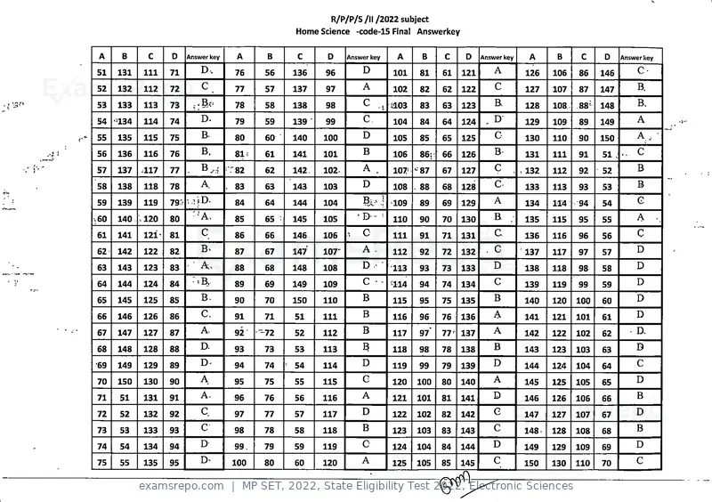
Text of page 15
R/P/P/S /II /2022 subject
                                                                 Home Science -code-lS Final Answerkey


        A    B      C     D      Answer key     A     B           C      D     Answer key    A      B    C     D    Answer key     A      B      C    D      Answerkey

       51    131   111    71         D.        76    56          136    96         D        101    81    61   121       A         126    106    86    146        G-

       52    132   112    72         C         77    57          137    97         A        102    82    62   122       C         127    107    87    147        B.

       53    133   113    73                   78    58          138    98         c .. a03        83    63   123       B         128    108-   88-   148        B,

       54 •^134    114    74         D.        79    59          139'   99         C        104    84    64   124       D'        129    109    89    149        A

       55    135   115    75         B-        80    60          140    100        D        105    85    65   125       O         130    110    90    150        A, -

       56    136   116    76         B.        81;   61          141    101        B        106          66   126       B-        131    111    91    51 ,       G

-/ 5   57    137   .117   77                  ; 82   62          142    102'       A .      107' ^87     67   127       C        . 132   112    92    52         B

       58    138   118    78         A        . 83   63          143    103        D        108 . 88     68   128       C-        133    113    93    53         B

       59    139   119    79''                 84    64          144    104        Bv^ i -109      89    69   129       A         134    114    94    54         G

       ^60   140 ■120     80       - 'A.       85     65 :       145    105       ^D - ^    110    90    70   130      B          135    115    95    55         A

       61    141   121•   81         C         86     66         146    106        C        111    91    71   131       C         136    116    96    56         C

       62    142   122    82         B^        87     67         147    107'       A .      112    92    72   132    . 0          137    117    97    57         D

       63    143   123    83     - ■ A.        88     68         148    108        D ^      ■113   93    73   133      D          138    118    98    58         D

       64    144   124    84      -B,.         89    69          149    109        C -" ^114       94    74   134       C         139    119    99    59         D

       65    145   125    85         B.        90    70          150    110        B        115    95    75   135      B          140    120    100   60         D

       66    146   126    86         C.        91    71          51     111        B        116    96    76   136       A         141    121    101   61         D

       67    147   127    87         A         92    -72         52     112        B        117    97^   77^ 137        A         142    122    102   62         D.

       68    148   128    88         D.        93    73          53     113        B,       118    98    78   138      B          143    123    103   63         D

       '69   149   129    89         D-        94    74      =   54     114        D        119    99    79   139      D          144    124    104   64         G

       70    150   130    90         A         95    75          55     115        G        120    100   80   140       A         145    125    105   65         D

       71    51    131    91         A.        96    76          56     116        A        121    101   81   141      D          146    126    106   66         B

       72    52    132    92         C         97    77          57     117        D        122    102   82   142      G          147    127    107   67         D
                                                                                                    00
       73    53    133    93         C         98    78          58     118        B        123    103   83   143      G          148    128    108   68         B

       74    54    134    94         D'        99.   79          59     119        C        124    104   84   144      D          149    129    109   69         D

       75    55    135    95         D-        100   80          60     120        A        125    105   85   145      G          150    130    110   70         G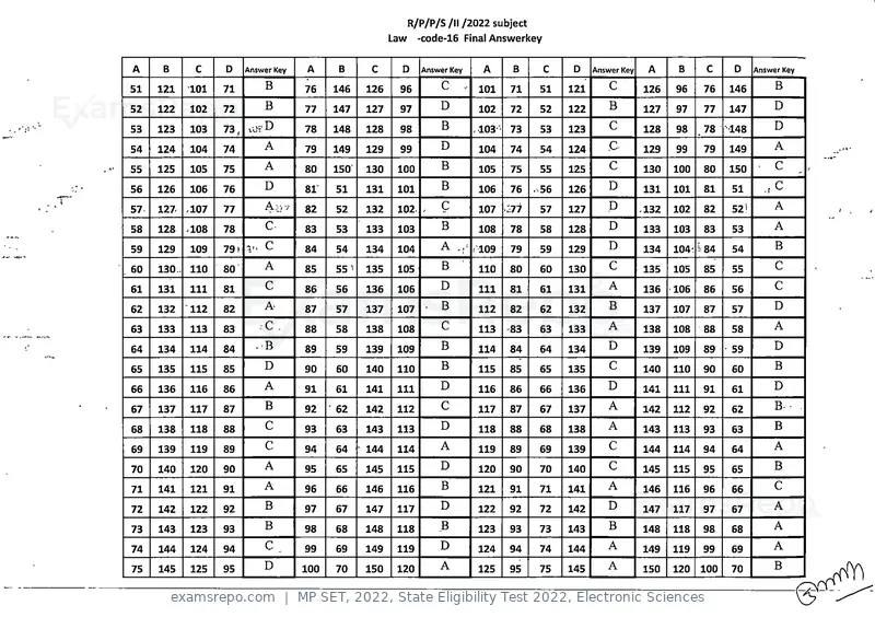
Text of page 16
R/P/P/S /II /2022 subject
                                                           Law 'Code-16 Final Answerkey


A     B      C     D      Answer Key    A     B      C       D    Answer Key     A        B     C     D    Answer Key    A      B     C      D      Answer Key

51   121    101    71         B        76    146    126      96       c    . 101         71     51   121      c         126    96    76     146          B

52   122    102    72         B        77    147    127      97       D         102      72     52   122      B         127    97    77     147          D

53   123    103    73. lUr D           78    148    128      98       B        . 103 ■   73     53   123      C         128    98    78    ■•■148       D

54   124    104    74         A        79    149    129      99       D         104      74     54   124      .c        129    99    79     149          A

55   125    105    75         A        80    150    130     100       B         105      75     55   125      c         130    100   80     150          C

56   126    106    76         D        81    51     131     101       B         106      76    .56   126      D         131    101   81      51       ..c
57   127-   .107   77         Ac/V     82    52     132     102. ,    C         107      ^77    57   127      D         .132   102   82      52'         A

58   128    .108   78         C        83    53     133     103       B         108      78     58   128      D         133    103   S3      53          A

59   129    109    79 s   in C         84    54     134     104       A .n ilOS          79     59   129      D         134    104'. i84     54          B

60   130.. 110     80         A        85    55^    135     105       B         110      80     60   130      C         135    105   85      55          C

61   131    111    81         C        86    56     136     106       D         111      81     61   131       A        136    106   86      56          C

62   132    112    82         A        87    57     137     107   .   B         112      82     62   132      B         137    107   87      57         D

63   133    113    83        ,C .      88    58     138     108       C         113      83     63   133      A         138    108   88      58          A

64   134    114    84       - B        89    59     139     109       B         114      84     64   134      D         139    109   89      59         D

65   135    115    85         D        90    60     140     110       B         115      85     65   135      C         140    110   90      60          B

66   136    116    86         A        91    61     141     111       D         116      86     66   136      D         141    111   91      61         D

67   137    117    87         B        92    62     142     112       C         117      87     67   137      A         142    112   92      62          B.

68   138    118    88         C        93    63     143     113       D         118      88     68   138      A         143    113   93      63         B

69   139    119    89         C        94    64    ' 144    114       A         119      89     69   139      C         144    114   94      64          A

70   140    120    90         A        95    65     145     115       D         120      90     70   140      C         145    115   95      65         B

71   141    121    91         A        96    66     146     116       B         121      91     71   141      A         146    116   96      66          C

72   142    122    92         B        97    67     147     117       D         122      92     72   142      D         147    117   97      67          A

73   143    123    93         B        98    68     148     118       ,B        123      93     73   143      B         148    118   98      68          A

74   144    124    94         C.       99    69     149     119       D         124      94     74   144      A         149    119   99     69          A

75   145    125    95         D        100   70     150     120       A         125      95     75   145      A         150    120   100    70          B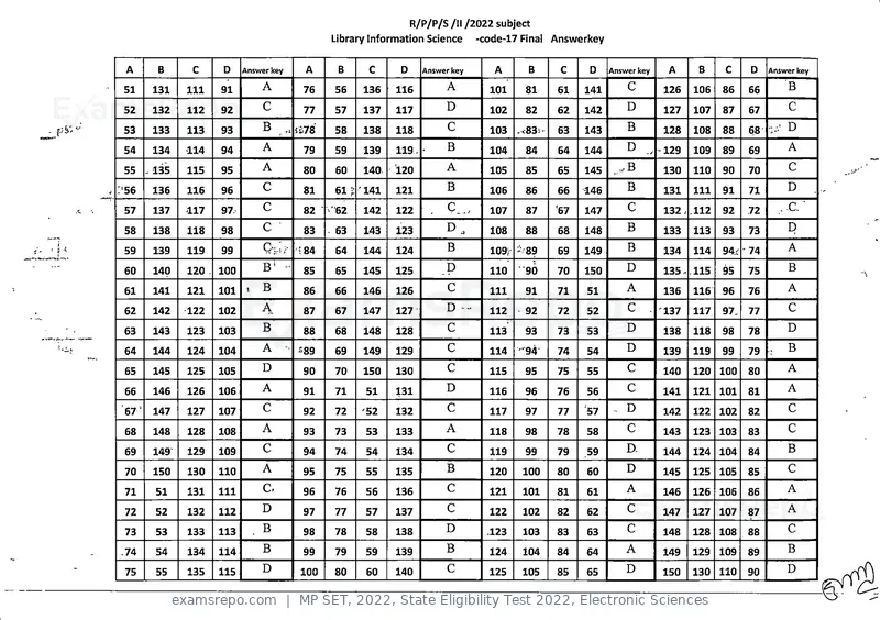
Text of page 17
R/P/P/S /II /2022 subject
                                                    Library Information Science       -code-17 Final Answerkey


 A      B      C     D     Answer key         A      B       C     D     Answer key      A      B     C    D     Answer key    A      B     C    D    Answer key

 51    131    111    91         A            76     56      136   116         A         101     81   61    141       c         126   106   86    66       B

 52    132    112    92         C            77     57      137   117         D         102     82   62    142       D         127   107   87    67       C

 53    133    113    93         B           i;i78   58      138   118         C         103 .^83i-   63    143       B         128   108   88    68       D

 54    134    -114   94         A            79     59      139   119.        B         104     84   64    144       D        -129   109   89    69       A

 55 ,135      115    95         A            80     60      140   120         A         105     85   65    145       B         130   110   90    70       C

?56    136    116    96         C            81     61 ■:   141   121         B         106     86   66    146       B        131    111   91    71       D

 57    137    117    97         C             82    '62     142   122                   107     87   '67   147       C        132. .112    92    72    , C. ~
 58    138    118    98         c             83    63      143   123         D.        108     88   68    148       B         133   113   93    73       P
 59    139    119    99         cn,:.               64      144   124         B         109.i '89    69    149       B         134   114   94.C '74       A

 60    140    120 . 100                 -
                                              85    65      145   125         P         110     90   70    150       D        135. .115    95    75       B

 61    141    121    101    >   B             86    66      146   126         C         111     91   71    51        A         136   116   96    76       A

 62    142    122    102        A             87    67      147   127         D         112     92   72    52        C    .    137   117   97,   77       C

 63    143    123    103        B             88    68      148   128         C         113     93   73    53        D         138   118   98    78       D

 64    144    124    104        A       -   ^89     69      149   129         C         114    "94   74    54        D         139   119   99    79       B

 65    145    125    105        D             90    70      150   130         c         115     95   75    55        C        140    120   100   80       A

 66    146    126    106        A             91    71      51    131         D         116     96   76    56        C        141    121 101     81       A

 67'   147    127    107        C             92    72      '52   132         C         117     97   77    57     - D         142    122   102   82       C

 68    148    128    108        A             93    73      53    133         A         118     98   78    58        C        143    123   103   83       C

 69    149'   129    109        C             94    74      54    134         C         119     99   79    59        D-       144    124   104   84       B

 70    150    130    110        A             95    75      55    135         B         120    100   80    60        D        145    125   105   85       C

 71    51     131    111        C-            96    76      56    136         C         121    101   81    61        A        146    126   106   86       A

 72    52     132    112        D             97    77      57    137         C         122    102   82    62        C        147    127   107   87       A

 73    53     133    113        B             98    78      58    138         D         .123   103   83    63        C        148    128   108   88       C

.74    54     134    114        B             99    79      59    139         B         124    104   84    64        A        149    129   109   89       B

 75    55     135    115        D            100
                                              00    80      60    140         C         125    105   85    65        D        150    130   110   90       D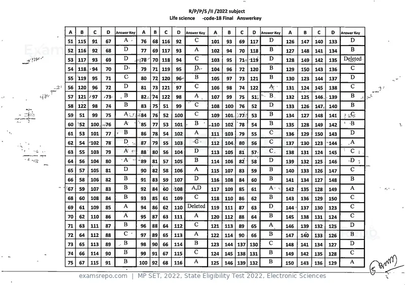
Text of page 18
R/P/P/S /II /2022 subject
                                                         Life science      -code-18 Final Answerkey


    A     B     C     D     Answer Key    A    B    C       D     Answer Key    A      B     C      D    Answer Key    A       B     C     D    Answer Key

    51   115   91    67         A .      76    68 116      92         c        101    93    69     117       D        126     147   140   133        D

    52   116   92    68         D        77    69 117      93         A        102    94    70     118       B        127     148   141   134        B

i   53   117   93    69         D        >78   70 118      94         C        103    95           119       D        128     149   142   135    Dejeted •
    54   118. -94    70         D.       79    71 119      95         P-'      104    96    72     120       B        129     150   143   136        C

    55   119   95    71         C        80    72 120      96>^       B        105    97    73     121       B        130     123   144   137        D

    56   120   96    72         D        81    73 121      97         C        106    98    74     122       A: ■     131     124   145   138        C

    57   121 -97     ^^73     ^B         82." 74 122       98         A ^      107    99    75     51;       B.       132     125   146. 139         B

    58   122   98    74         B        83    75   51     99     ' C          108    100   76     52        n        133     126   147^ 140         B

    59   51    99    75         A:,/, ->84     76   52     100        C        109    101. ;.77:   53        B        134     127   148   141

    60   52    100, ^-76        A     ^ '85    77   53     101        B     • ..110   102   78     54        B        135     128   149   142    = -B

    61   53    101   77     . B          86    78   54     102        A        111    103   79     55        c        136     129   150   143        D

    62   54    102   78        D         87    79   55     103        G-       112    104. 80      56        c        137     130   123 -144         ,A
    63   55    103   79         A .-     88    80   56     104        D        113    105   81     57       c.        138     131   124   145    ■   C ;,
    64   56    104   80       -A - "89         81   57     105        B        114    106   82'    58       D         139     132   125   146        D.

    65   57    105   81        D         90    82   58     106        A        115    107   83     59        B        140     133   126   147        c

    66   58    106   82         B        91    83   59     107        D        116    108   84     60       B         141     134   127   148        B

    67   59    107   83         B        92    84   60    -108      A,D        117    109   85     61       A         142     135   128   149        A

    68   60    108   84        B         93    85   61     109        C        118    110   86     62       B         143     136   129   150        C

    69   61    109   85        A         94    86   62     110    Deleted      119    111   87     63       D         144 =   137   130   123        C

    70   62    110   86        A         95    87   63     111        A        120    112   88     64       B         145     138   131   124        C

    71   63    111   87        B         96    88   64    112         C        121    113   89     65       A         146     139   132   125        D

    72   64    112   88        c -       97    89   65    113         A        122    114   90     66       B         147     140   133   126        B

    73   65    113   89     ,B           98    90   66    114         B        123    144   1371■ 130       C         148     141   134   127        D

    74   66    114   90         B'       99    91   67    115         C        124    145   138    131      B         149     142   135   128        C

    75   67    115   91        B         100   92   68    116         A        125    146   139 132         B         150     143   136   129        A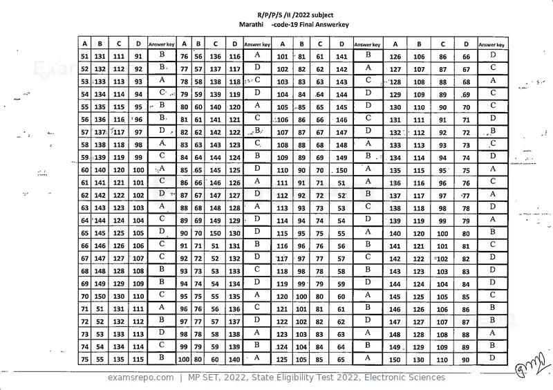
Text of page 19
R/P/P/S /II /2022 subject
                                                             Marathi       -code-19 Final Answerkey


A     B      C      D     Answer key    A    B     C     D    Answer key     A       B     C       D    Answer key      A       B     C      D    Answer key

51   131    111    91         B        76   56    136   116           A     101           61      141       B          126     106    86    66           D

52   132    112    92         B-       77   57    137   117           D     102     82    62      142       A          127     107    87    67           C

53. il33    113    93         A        78   58    138   118 ;v-C            103     83    63      143       C        ^ ■128    108    88    68            A

54   134    114    94         C        79   59    139   119           D     104     84    -64     144       D          129     109    89    .69           C

55   135    115    95 .      B         SO   60    140   120           A     105    V.85   65      145       D          130     110    90    70            C

56   136    116.   '96        B.       81   61    141   121           C    .:106    86    66      146       C          131     111    91    71           D

57   137. ^117     97        D ..      82   62    142   122       ..A-      107     87    67      147       D          132 . - 112    92    72     •
                                                                                                                                                         B
                                                                                                                                                       tt .


58   138    118    98         A.       83   63    143   123           c     108     88    68      148       A          133     113    93    73            C

59. = 139   119    99         C        84   64    144   124           B     109     89    69      149       B .T , 134         114    94    74           D

60   140    120    100      >.A        85   -65   145   125           D     110     90    70    . 150       A          135     115    95    75           A

61 141      121    101        C        86   66    146   126           A     111     91    71      51        A          136     116    96    76           C

62   142    122    102       D 7< 87        67    147   127           D     112     92    72      52        B          137     117    97    77           A

63   143    123    103        A        88   68    148   128   ■       A     113     93    73      53        C          138     118    98    78           D

64 ■144     124    104        C        89   69    149   129   .       D     114     94    74      54       D           139     119    99    79           A

65   145    125    105       D         90   70    150   130           D     115     95    75      55        A          140     120   100    80           B

66   146    126    106        C        91   71    51    131           B     116     96    76      56       B           141     121   101    81           C
                                                                                    00
67   147    127    107        C        92   72    52    132           D     117     97    77      57        C          142     122   =102   82           D

68   148    128    108       B         93   73    53    133           C     118     98    78      58        B          143     123   103    83           D

69   149    129    109       B         94   74    54    134           D     119     99    79      59       D           144     124   104    84           D

70   150    130    110        C        95   75    55    135           A     120    100    80      60        A          145     125   105    85           C

71   51     131    111        A        96   76    56    136           C     121    101    81      61        B          146     126   106    86           B

72   52     132    112       B         97   77    57    137           D     122    102    82      62       D           147     127   107    87           B

73   53     133    113       D         98   78    58    138           A     123    103    83      63        A          148     128   108    88           A

74   54     134    114       C         99   79    59    139           B     .124   104    84      64       B           149 ,   129   109    89           B

75   55     135    115       B         100 80     60    140       •   A     125    105    85      65        A          150     130   110    90          D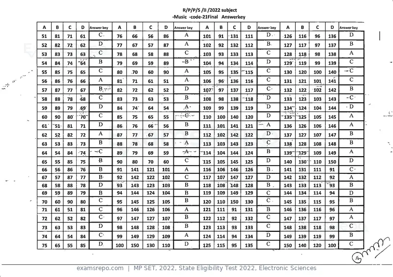
Text of page 20
R/P/P/S /II /2022 subject
                                                              -Music -code-21Flnal Answerkey

A     B     C      D     Answer key   A      B     C    D     Answer key     A      B     C      D     Answer key    A      B      C     D     Answer key

51   81     71     61        c.       76    66    56    86         A        101    91    ■131   111        D.       126    116    96    136         D-

52   82     72     62        D        77    67    57    87         A        102    92    132    112        B.       127    117    97    137         B

53   83     73     63     „ C         78    68    58    88         C       . 103   93    133    113        C        128    118    98    138         A

                             B                                    ..B- -                                   D                                        C
54   84     74    ""64                79    69    59    89                  104    94    134    114                 129    119    99    139

55   85     75     65        C        80    70    60    90         A        105    95    135 -^115         C        130    120    100   140      -C

56   86     76     66        A        81    71    61    51         A.       106    96    136    116        C        131    121    101   141         c

57   87     77     67        Bt'      82    72    62    52         D        107'   97    137    117        c-       132    122    102   142         B

58   88     78     68        C        83    73    63    53        B         108    98    138    '118     "D         133    123    103   143       "C

59   89     79    -69        D        84    74'   64    54         A-       109    99    139    119        D        134" 124      104   144       - D

60   90     80'    io'       C        85    75    65    55                  110    100   140    120        D        -135^ "125    105   145         A

61   •51-   81     71        D        86    76    66    56         B        111    101   141    121        A        136    126    106   146         A

62   52     82     72        A        87    77    67    57         B        112    102   142    122        D        137    127    107   147         B

63   53     83     73        B        88    78    68    58       - A        113    103   143    123        C        138    128    108   148         B

64   54     84     74
                         - ^'C        89    79    69    59        -A"-     '114    104   144    124        B        139"   229'   109   149         A

65   55     85     75        B        90    80    70    60         C        115    105   145    125        D        140    130 - 110    150         D

66   56     86     76        B        91    141   121   101        A        116    106   146    126        B.       141    131    111    91         C'
67   57     87     77        B        92    142   122   102        C        117    107   147    127        D        142    132    112    92         A

68   58     88     78        D        93    143   123   103        B        118    ios" 148     128        B ..     143    133    113   ''93        B

69   59     89     79        B        94    144   124   104        B        119    109   149    129        C        144    134    114    94         D

70   60     90     SO        C        95    145   125   105        B        120    110   150    130        C        145    135    115    95         B

71   61     51     81        C        96    146   126   106        A        121    111    91    131        B        146    136    116    96         A

72   62     52     82        C        97    147   127   107        B        122    112    92    132        C        147    137    117    97         A

73   63     53     83        D        98    148   128   108        B        123    113    93    133        C        148    138    118    98         C

74   64     54     84        C        99    149   129   109        A        124    114    94    134        D        149    139    119    99         B

75   65     55     85        D        100   150   130   110        D        125    115    95    135        C        150    140    120   100         C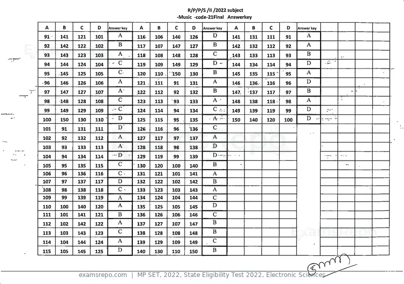
Text of page 21
R/P/P/S /II /2022 subject
                                                          -Music -code-21Flnal Answerkey

A       B     C     D    Answer key        A       B     C          D    Answer key    A         B      C     D     Answer key

91     141   121   101         A          116     106   146        126        D       141       131    111    91        A

92     142   122   102         B          117     107   147        127        B       142       132    112    92        A

93     143   123   103         A          118     108   148        128        C       143       133    113    93        B                ^.


94     144   124   104     - C            119     109   149        129        D -     144       134    114    94        D

95    .145   125   105         c.         120     110 . '150       130        B       145       135    115^   95        A                     -


96     146   126   106         A          121 .   Ill    91        131        A       146       136    116    96        D

97     147   127   107         A'         122     112    92        132        B       147,      ■137   117    97        B

98     148   128   108         C          123     113    93        133        A •     148       138    118^   98        A                -


99     149   129   109     .- C           124     114    94        134        C       149       139    119    99        D
                                                                            . A- -■
100    150   130   110 ^ . '   D          125     115    95    -   135                150       140    120    100       D

101    91    131   111         D'         126     116    96        136        C

102    92    132   112         A          127     117    97        137        A

103    93    133   113         A-         128     118    98        138        D

104    94    134   114         -B     '   129     119    99        139       D-r        -   .                                    —   -


105    95    135   115         C          130     120   100        140        B             -


106    96    136   116         C ^        131     121   101        141        A
107    97    137   117         D          132     122   102        142        B

108    98    138   118         C ^        133     123   103        143        A
109    99    139   119         A          134     124   104        144        C

110    100   140   120         A          135     125   105        145        D

111   101    141   121         B          136     126   106        146        C

112    102   142   122         A          137     127   107        147        B

113    103   143   123         C          138     128   108        148        B

114    104   144   124         A          139     129   109        149        C

115    105   145   125         D          140     130   110        150        B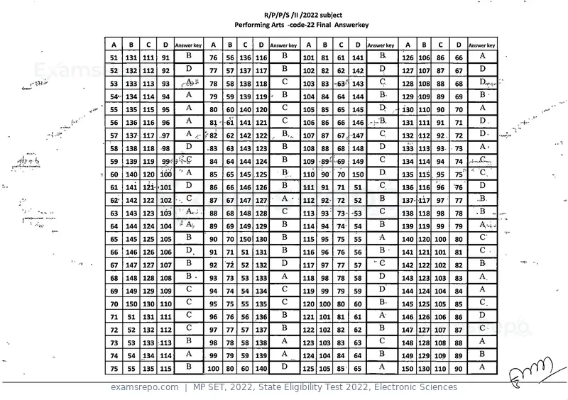
Text of page 22
R/P/P/S /II /2022 subject
                                                Performing Arts -code-22 Final Answerkey


A     B      C    D     Answer key    A    B      C    D    Answer key    A     B     C    D     Answer key    A   B     C    D    Answer key

51    131 111     91        B        76    56 136 116           B        101    81   61    141       B.       126 106    86   66           A

52    132 112     92        D        77    57 137 117           B        102    82   62    142       P        127 107    87   67           D

53    133 113     93                 78    58 138 118           C        103    83   -63^^ 143       C.       128 108    88   68

54.^ 134 114      94        A        79    59    139 119 ..     B        104    84   64    144       B.       129 rl09   89   69           B

55    135   115   95        A        80    60 140 120           C        105    85   65    145       P-       130 110    90   70           A

56    136 116     96        A        81- -61     141 121        C        106    86   66    146   .-r'B-       131 111    91   71           D.        ..4-


57    137 117 ,97           A.r r82        62 142 122                    107    87   67, 147         C,       132 112    92   72           D.
                                                                                                                                                            1
58    138 118     98        D        .83   63 143 123           B        108    88   68    148       D        133 113    93   73           A-

59    139 119     99^ ?              84    64 144 124           B        109         -69   149       C        134 114    94   74   .'*4'         1


60    140 120 100           A        85    65 145 .125          B:.      lid    90    70   150       D.       135 115    95   75      ■ c.
61    141   lii '101        D        86    66    146 126        B        I'll   91   71    51        C.       136 lie    96   76           D

62*   142 122 102       ', c         87    67 147 127 ■         A'. 112 92           72    52        B        137- 117   97   77           -B.

63    143 123     103       A,J.     88    68    148 128        C        113    93^ 73 -53           C        138 118    98   78       .B

64    144 124 104                    89    69 149 129           B        114    94   74-   54        B        139 119    99   79

65    145   125   105       B        90    70 150 130           B        115    95   75    55        A        140 120 100     80           c-

66    146 126     106       D,       91    71    51   131       B        116    96   76    56        B •      141 121 101     81           c .
                                                                                                 .


67    147 127 107           B        92    72    52   132       D        117    97   77    57                 142 122 102     82           B

68    148 128     108       B.       93    73    53   133       A        118    98   78    58        D        143 123 103     83           A,

69    149   129   109       C        94    74    54   134       C        119    99         59        D        144 124 104     84           A
                                                                                     79

70    150 130 110           C        95    75    55   135       C        120 100     80    60        B^       145 125 105     85           C.

71    51    131   111      c         96    76    56   136       B        121 101     81    61        A        146 126 106     86           D
                                                                             do
72    52    132 112        c         97    77    57   137       B        122 102     82    62        B        147 127 107     87           C

73    53    133 113         B        98    78    58   138       A        123 103     83    63        C        148 128 108     88           A

74    54    134   114       A        99    79    59   139       A        124 104     84    64        B        149 129 109     89           B

75    55    135   115       B        100   80    60   140       D        125 105     85    65        A        150 130 110     90           A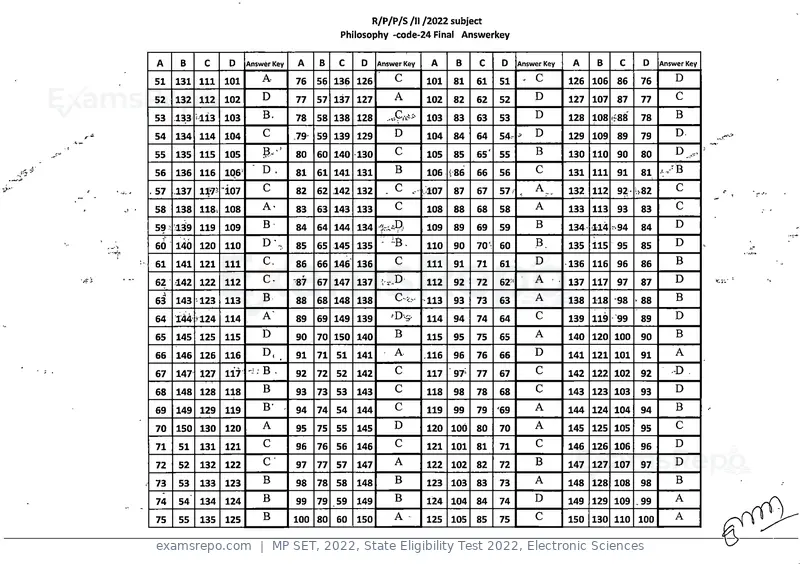
Text of page 23
R/P/P/S /II /2022 subject
                                                   Philosophy -code-24 Final Answerkey


 A         B     C    D     Answer Key   A    B    C    D     Answer Key      A     B     C     D    Answer Key   A     B     C      D      Answer Key

 51       131   111   101       A        76   56 136 126               c     101    81    61   51    . c          126 106     86    76          D

 52       132 112     102       D        77   57 137 127               A     102    82    62   52        D        127 107     87    77          C

 53       133 -113    103       B.       78   58 138 128                     103    83    63   53        D        128 108 fi88      78          B

 54       134 114     104       C        79   59 139 129               D     104    84    64   54^.      D        129 109     89    79          D.

                                B.-                                    C                                 B                             CO       D
 55       135 115     105                80   60 140 130                     105    85    65' 55                  130 110 90        80
                                                                                                                                    OC
                                                                                                                                    00

 56       136 116     106' ' D .         81   61 141 131               B     106 ■ 86     66   56        C        131   111   91    81      .w-B

. 57 .137       1175 ^i07       C        82   62 142 132       .c            107    87    67   57        A        132 112     92'
                                                                                                                                                C

 58       138 118. 108          A-       83   63 143 133               C     108    88    68   58        A        133 113     93    83          C

 59^ >139 119         109       B        84   64 144 134                     109    89    69   59        B        134 H4"94         84          D

 60       146 120     110       D\.      85   65 145 135       - -B.         110    90    70- 60         B.       135 115     95    85          D

 61       141 121     111       C.       86   66 146' 136              C     111    91    71   61        D        136   116   96    86          B

 62 142 122           112       C-       87   67 147 137      .•.„D
                                                               t   A         112    92    72   62:       A    ■ . 137 117 97        87          D
  A   ■
 63       143 123     113       B        88   68 148 138                     113    93    73   63        A        138 118 '98                   B

 64       144 rl24    114       A'       89   69 149 139                     114    94    74   64        C        139 119     99    89          D

 65       145 125     115       D        90   70 150 140               B     115    95    75   65        A        140 120 100       90          B

 66       146 126     116                91   71   51   141            A     .116   96    76   66        D        141 121 101       91          A
                                     .


 67       147 127     117   ^j. B .      92   72   52   142            C     117    97'   77   67        C        142 122 102       92         -D ,

 68       148 128     118       B        93   73 53     143            C     118    98    78   68        C        143 123 103       93          D

 69       149 129     119       B' . 94       74   54   144            C     119    99    79   ^69       A        144 124 104       94          B

 70       150 130     120       A        95   75   55   145            D     120 100      80   70        A        145 125 105       95          C

 71       51    131   121       C        96   76   56   146            C     121    101   81   71        C        146 126 106       96          D

 72       52    132   122       C        97   77   57   147            A     122 102      82   72        B        147 127 107       97          D

 73       53    133   123       B        98   78   58   148            B     123    103   83   73        A        148 128 108       98          B

 74       54    134   124       B        99   79 .59    149            B     124 104      84   74        D        149 129 109 . 99              A

 75       55    135   125       B        100 80    60   150            A ■   125    105   85   75        C        150 130 110       100         A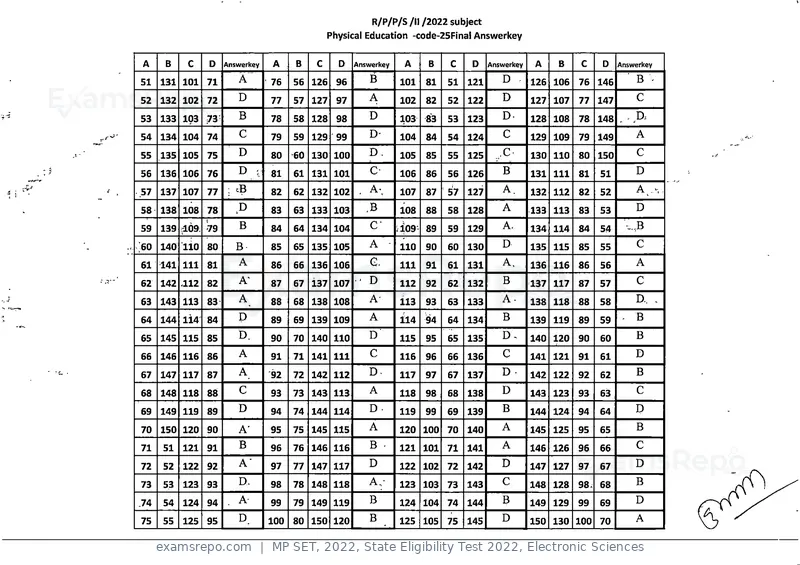
Text of page 24
R/P/P/S /II /2022 subject
                                                  Physical Education -code-25Final Answerkey


 A     B    C     D    Answerkey   A     B    C     D   Answerkey    A    B    C    D     Answerkey   A    B    C    D     Answerkey

51    131 101     71      A        76    56 126    96      B        101   81   51   121      D .      126 106   76 146         B'

52    132 102     72      D        77    57 127    97      A        102   82   52   122      D        127 107   77 147         C

53 133 103 73             B        78    58 128 98         D        103   83   53   123      D-       128 108   78 148     . - D.
54    134 104     74      C        79    59 129    99      D-       104   84   54   124      C        129 109   79 149         A

55    135 105     75      D        80    60 130 ICO        D.       105   85   55   125      C        130 110   80   150       C

56    136 106 76          D ;      81    61 131 101        c-       106   86   56   126      B        131 111   81   51        D

.57   137 107 77       ; .B        82    62 132 102         A-.     107   87   57   127      A.       132 112   82   52        A..V
58 138 108 78                      83    63 133 103       ,B        108   88   58   128      A        133 113   83   53        D

59    139 -109: '79       B        84    64 134 104        C        409   89   59   129      A,       134 114   84   54

'SO 140 110 80           B-        85    65 135 105        A        110   90   60   130      D        135 115   85   55        C

61 141 111        81      A        86    66 136 106         G.      111   91   61   131      A.       136 116   86   56        A

62    142 .112 82         A'       87    67   i37 107 ■ D           112   92   62   132      B        137 117   87   57        C

63 143 113 83             A        88    68 138 108        A        113   93   63   133      A.       138 118   88   58        D.. ,

64    144   li4   84      P        89    69 139 109        A        114   94   64   134      B        139 119   89   59    .   B

65    145 115 85          D.       90    70 140 110        D        115   95   65   135      D-       140 120   90   60        B

66    146 116     86      A        91    71 141 111        C        116   96   66   136      C        141 121   91   61        D

67    147 117 87          A        92    72 142 112        D.       117   97   67   137      D'       142 122   92   62        B

68    148 118 88          C        93    73 143 113        A        118   98   68   138      D        143 123   93   63        C

69    149 119     89      D        94    74 144 114        D.       119   99   69   139      B        144 124   94   64        D

70    150 120 90          A'       95    75 145 115        A        120 100 70      140      A        145 125   95   65        B

71    51    121   91      B        96    76 146 116        B -      121 101    71   141      A        146 126   96   66        C

72    52    122 92        A"       97    77 147 117        D        122 102 72      142      D        147 127   97   67        D

73    53    123   93      D-       98    78 148 118        A,-      123 103    73   143      C        148 128   98. 68         B

74    54    124   94      A        99    79 149 119        B        124 104    74   144      B        149 129   99   69        D

75    55    125 95                 100   80 150 120        B        125 105    75   145      D        150 130 100    70        A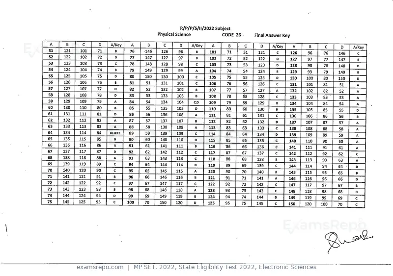
Text of page 25
R/P/P/S/l1/2022 Subject
                                              Physical Science                 CODE 26        Final Answer Key

 A    B     C     D     A/Key     A     B       C       D        A/Key    A      B        C     D     A/Key       A     B     C       D        A/Key
51   121   101   71       B       76   ■146    126      96        B      101    71       51    121     C         126    96   ■76     146        c
52   122   102   72       D       77   147     127      97        6      102    72       52    122     D      127       97    77     147        B
53   123   103   73       C       78   148     128      98        c      103    73       53    123     D      128       98    78     148        D
54   124   104   74 .     B       79   149     129     99         A      104    74       54    124     B      129       99    79     149        B
55   125   105   75       D       80   150     130     100        c      105    75       55    125     D      130      100    80     150        0
56   126   106   76       B       81    51     131     101        c      106    76       56    126     c      131      101    81     51         A
57   127   107   77       D       82    52     132     102        B      107    77       57    127     A      132      102    82     52         A
58   128   108   78       D       83    53     133     103        B      108    78       58    128     C      133      103    83 "   53         A
59   129   109   79       A       84    54     134     104       C,D     109    79       59    129     B      134      104    84     54         A
60   130   110   80       B      85     55     135     105        D      110    80       60    130     B      135      105    85     55         D
61   131   111   81       D      86    56      136     106        A      111    81       61    131     C      136      106    86     56         B
62   132   112   82       A      87    57      137     107        8      112    82       62    132     D      137      107    87     57         A
63   133   113   83       A      88    58      138     108        A      113    83       63    133     C      138      108   88      58         A
64   134   114   84     DELETE   89    59      139     109        c      114    84       64    134     D      139      109   89      59         A
65   135   115   85       B      90    60      140     110        D      115    85       65    135     C      140      110   90      60         A
66   136   116   86       A      91    61      141    111         6      116    86       66    136     C      141      111   91      61         A
67   137   117   87       D      92    62      142    112         C      117    87       67    137     c      142      112   92      62         C
68   138   118   88       A      93    63      143    113         c      118    88       68    138     B      143      113   93      63         A
69   139   119   89       C      94    64      144    114         B      119    89       69    139     C      144      114   94      64    ■    0
70   140   120   90       c      95    65      145    115         A      120    90       70   140      B      145      115   95      65         B
71   141   121   91       B      96    66      146    116         8      121    91       71   141      A      146      116   96      66         D
72   142   122   92       C      97    67      147    117         C      122    92       72   142      C      147      117   97      67         B
73   143   123   93       B      98    68      148    118         A      123    93       73   143      C      148      118   98      68        D
74   144   124   94      D       99    69      149    119         B      124    94       74   144      D      149      119   99      69        C
75   145   125   95       C      100   70     150     120         D      125    95       75   145      C      ISO      120   100     70        C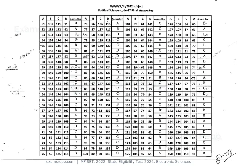
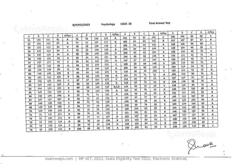
Text of page 27
Psychology       CODE 28   Final Answer Key
R/P/P/11/2022


                         B,C,D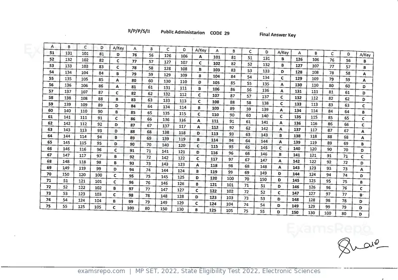
Text of page 28
R/P/P/S/II   Public Administarion CODE 29
                                            Final Answer Key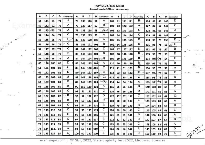
Text of page 29
R/P/P/S /II /2022 subject
                                                 Sanskrit-code-30Final Answerkey

A     B     C    D    Answerkey     A     B      C     D     Answerkey    A    B     C     D     Answerkey    A      B     C     D    Answerkey

51   111   91    71      A          76   136    116   96         A       101   61   141   121       B-       126                          D
                                                                                                                    86    66    146

52   112   92    72      A          77   137    117   97         B       102   62   142 122         A        127    87    67    147       C

53   113 iJ93    73      A          78   138    118   98                 103   63   143 123         C        128    88.,68^ 148           A

54   114   94    74      C          79- 139     119   99         A       104   64   144 124       - C        129    89    69    149       A

55   115   95    75                 80   140    120   100        A.      105   65   145 125         D        130    90    70    150       D

56   116   96    76                 81   141    121   101        B       106, 66    146 126         D        131    91    71    51        c

57   117   97:ni         c          82 -142 .122      102        c       167' 67    147 127^        D.       132    92    72. :52'        B

58   118   98    78      B     ■    83   143    123   103        B       108   68   148 128         B        •133   93          53        D
                                                                                                                          73

59   =119^ 99    79      A          84   144    124   1045                                          B                                     G
                                                             w   -       109   69   149 129                  134    l94> ri74   54

60   120   100   80      D     t    85   145°   125   105        A       110   70   150 130                  135 '95      75    55        B

61   121   101   81      C          86   146    126' ^106        C       111   71   51    131       B        136    96    76    56        A

62   122   102   82      D          87- 147     127   107-               112   72   52    132^      C    - 137 -97i       77              C
                                                                                                                                57

63   123   103   83      A          88   148    128   108                113   73   53    133       C        138    98    78' 58          D

64   124' 104    84      B          89   149    129   109                114   74   54    134       A                                     A
                                                                                                             139    99- "79     59

65   125   105   85      B          90   150    130   110        A       115   75   55    135       B        140 100      80              C
                                                                                                                                60

66   126   106   86      C          91   51     131   111        C       116   76   56    136       D        141 101      81    .61       A

67   127   107   87    <.B •        92   52     132   112        D       117   77- 57     137       C        142 102                      e.
                                                                                                                          82    62

68   128   108   88      B          93   53     133   113        C       118   78   58    138       A        143 103     83               A
                                                                                                                                63

69   129   109   89      C.        "94   54     134   114        B       119   79   59    139       B        144 104     84     64        B

70   130   110   90      C         95    55     135   115        C       120   80   60    140       C        145 105      85              c
                                                                                                                                65

71   131   111   91      c          96   56     136   116        C       121   81   61    141       B        146 106      86    66        A

72   132   112   92      c         97    57     137   117        B       122   82   62    142       C        147 107     87               B
                                                                                                                                67

73   133   113   93      D         98    58     138   118        C       123   83   63    143       C                                     A
                                                                                                             148 108     88     68

74   134   114. 94       A         99    59     139   119        A       124   84   64    144       A        149 109                      D
                                                                                                                         89     69

75   135   115   95                100   60     140   120        B ■     125   85   65    145       C        150 110     90     70        A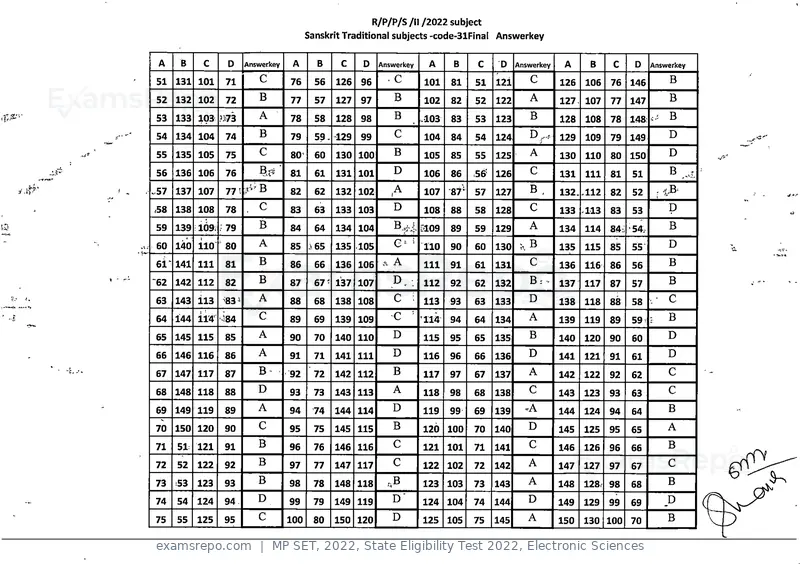
Text of page 30
R/P/P/S/ll/2022 subject
                                           Sanskrit Traditional subjects -code-31Final Answerkey

 A     B     C    D      Answerkey    A      B     C    D    Answerkey     A      B    C     D    Answerkey    A     B    C     D     Answerkey

 51   131 101     71        c        76      56   126   96     .c         101    81    51   121      c        126   106   76   146         B

 52   132 102     72        B        77      57   127   97          B     102    82    52   122      A        127   107   77   147         B

 53   133 103 ?i73          A        78      58   128   98          B    .103    83    53   123      B        128   108   78   148: ,.1    B

 54   134 104     74        B        79      59. 129    99          C     104    84    54   124      D,.. 129       109   79 149           D

 55   135 105     75        C        80      60   130 100           B     105    85    55   125      A        130   110   80   150         D

 56 136 106       76         B^^     81      61   131 101           D     106    86    56' 126       C        131   111   81   51          B

.57 137 107       77 \
                         :.p' B      82      62   132 102           A     107    87-   57   127      B.       132,.112    82   52      : iB
                                                                t


<58   138 108     78        C        83      63   133 103           D     108    88    58   128      C        133 .113    83   53          P
 59   139   id&< ; 79       B        84      64   134 104                a09     89    59   129      A        134   114                    B
                                                                                                                          84:: '54-

 60   140 110     80        A        85 j65       135 105                 110    90    60   130    xB         135   115   85   55          D

6i' 141 111       81        B        86      66   136 106           A     111    91    61   131      C        136   116   86   56          B

62    142 112     82        B        87     67' 137 107         D.        112    92    62   132      B: -     137   117   87   57          B

63 143      ii3             A        88     68    138 108           C   ; 113    93    63   133      D        138   118   88   58     .■   c
64    144   ii4 -)84        C        89     69    139 109       c       ■ "114   94    64   134      A        139   119   89   59 ;        B
65    145 115     85        A        90      70   140 110       D         115    95    65   135      B        140   120   90               D
                                                                                                                               60

66    146 116     86        A        91     71    141 111       D         116    96    66   136      D        141   121   91   61          D

67    147 117     87        B-       92     72    142 112       B         117    97    67   137      A        142   122   92   62          C

68    148 118     88        D        93     73    143 113       A         118    98    68   138      C        143   123   93               C
                                                                                                                               63

69 149 119        89        A        94     74    144 114       D         119    99    69   139     ^A        144   124   94   64          B
 V


70    150 120     90        C        95     75    145 115       B         120 100      70   140      D        145   125   95   65          A

71    51    121   91        B        96     76    146 116       C         121 101      71   141      C        146   126   96   66          B

72    52    122   92        B        97     77    147 117       C         122 102      72   142      A        147   127   97               C
                                                                                                                               67

73    53    123   93        B        98     78    148 118     .B          123 103      73   143      A        148   128. 98    68          B

74    54    124   94        D        99     79    149 119       D'        124 104      74   144      D        149   129   99   69          _D
75    55    125   95        C        100    80    150 120       D         125    105   75   145      A        150   130 100    70          B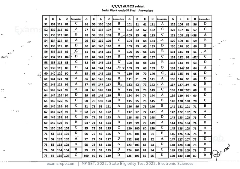
Text of page 31
R/P/P/S/II/2022 subject
                                               Social Work -code-32 Final Answerkey

 A     B    C     D   Answerkey    A    B     C      D     Answerkey        A     B     C     D    Answerkey    A     B          C      D     Answerkey

51    131 111    81      c        76    56   136    106       B            101   81     61   131      A        126   106        86      56         D

52    132 112    82      A        77    57   137    107       A            102   82     62   132      C        127   107        87      57         C

53    133 113 ^83        B        78    58   138    108                    403   83     63   133      C        128   108               -58         A

54    134 114    84      A        79    59   139    109       C            104   84     64   134      A        129   109        89      59         B

55    135 115    85      D        80    60   140    110       A            105   85     65 . 135      D        130   110        90      60         B

56    136 116    86    .Q-        81    61   141    111       A            106   86    '66   136      B        131   111        91OC    61
                                                                                                                                00            ..

                                                                                                                           l•


.57   137 117    .87i^ - D        82    62   142    112       B            107i- *87    67   137      C        132   112 . 92          .62'        C

58    138 118    88      C        S3    63   143 .113         D'           108   88     68   138      B        433   113        93      63.        D

59    139: 119   89      D        84    64   144    114                    109   89    69    139      D        134   114;;94            64         A

                         A                                   :A        -                              C                                            D
60    140' 12d   90               85^   65   145    115                    110   90     70   140               135   115        95      65

61    141 121    91      A        86    66   146    116       B            111   91     71   141      A        136   116    96          66         D

62    142 122    92      A        87    67   147    117       B..          112   92     72   142 ,    A        137   117- ^97           67         B

63    143 123    93      A        88    68   148    118       A            113   93     73   143      C        138   118 -98           68          B

64    144 124 !94        D        89    69   149    119       B--. 114           94    74    144      A        139   119 "99^          69          D

65    145 125    95      C        90    70   150    120       D            115   95    75    145      B        140   120   100          70         C

66    146 126    96      C        91    71   51     121       A            116   96    76    146      B        141   121   101          71         B

67    147 127    97      D        92    72   52     122       C            117   97    77    147      A        142   122 102            72         A   .

68    148 128    98      C        93    73   53     123       A            118   98    78    148      D        143   123   103          73         C

69    149 129    99      B        94 ' 74    54     124       D            119   99    79    149      A        144   124 104           74          B

70    150 130 100        C        95    75   55     125       C            120   100   80    150      C        145   125 105           75          A

71    51   131 101       D        96    76   56     126       A            121   101   81    51       B        146   126   106         76          B

72    52   132 102       A        97    77   57     127       D            122   102   82    52       A        147   127 107           77          D

73    53   133 103       A        98    78   58     128       A            123   103   83    53       D        148   128   108         78          B

74    54   134 104       B        99    79   59    , 129      D            124. 104    84    54       C        149   129 109           79          D

75    55   135 105       C        100   80   60     130       D            125   105   85    55       D        150   130   110         80          B      ^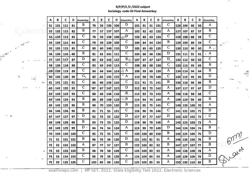
Text of page 32
R/P/P/S /II /2022 subject
                                                  Sociology -code-33 Final Answerkey


 A      B     C     D    Answerkey    A      B     C     D     Answerkey    A     B    C    D     Answerkey     A     B    C     D    Answerkey

 51    131   111   81         B       76    56    136   106     . D        101   81    61   131      c         126 106    86     56        A

 52    132   112   82         B       77    57    137   107       A        102   82    62   132      A         127 107    87     57        B

 53- -133' 113     83         C       78    58    138   108.               103   83    63   133      C         128 108           58        C

 54    134   114   84         C      .79    59    139   109       C        104   84    64   134      B         129 109    89     59        C

 55    135   115   85        ..c      80    60    140 110         D        105   85    65   135      C         130 110    90     60        A

 56    136   116 .86          B       81    61    141   111       C        106   86    66   136      D         131 111    91     61   , A
                                                                                                                            CO
                                                                                                                          00
 57. 137 •117      87         D       82    62    142 112         B<1.> 107 87         67   137      D.        132 112    921:62           C

 58    138   118   88         C '     83    63    143   113       C        108   88    68   138      a .       133 113    93     63        B

.59^ -■139   119   89         C       84    64    144   114:   ,4 A        109   89    69   139      A         134 114    94     64        B

 '60   140   120   90                 85    -65   145   115       A        110   90    70   140    .. c        135 115    95     65        D

 61    141 121     91         C       86    66    146   116       C        111   91    71   141      B        ■ 136 116   96     66        B

.62    142   122   92         C             67    147   117:      D        112   92    72   142      A         137 117    97     67        D

 63    143' 123    93         C       oo
                                      88    68    148   118                113                       A                                     C
                                       IX                                        93    73   143                138 118    98-    68

 64"^ 144    124   94         B       89    69    149   119                114   94    74   144      A         139   119' ■99    69        B

 65    145   125   95         B       90    70    150   120       B        115   95    75   145      C         140 120 100       70        A

 66    146   126   96         B       91    71    51    121       C        116   96    76   146      C         141 121 101       71        D

 67    147   127   97
                         -    D       92    72    52    122       D        li7   97    77   147      D         142 122    102    72    -   G

 68    148   128   98         B       93    73    53    123       D        118   98    78   148      A         143 123    103    73        A

 69    149   129   99         D .     94    74    54    124       A        119   99    79   149      D         144 124    104    74        B

 70    150   130   100        C       95    75    55    125       C        120 100     80   150      B         145 125    105    75        D

 71    51    131 101          B       96    76    56    126       D        121 101 81       51       A         146 126    106    76        B

 72    52    132   102        A       97    77    57    127       B .      122 102     82   52       B         147 127 107       77        B

 73    53    133   103        B       98    78    58    128       C        123 103     83   53       A         148 128    108    78        A

 74    54    134   104        C       99    79    59    129       A .      124 104     84   54       A        149 129     109 . 79         D

 75    55    135   105        C      100    80    60    130       C        125   105   85   55       A        150 130 110        80        B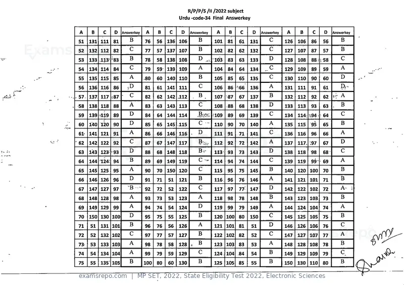
Text of page 33
R/P/P/S /II /2022 subject
                                                    Urdu -code-34 Final Answerkey

  A     B    C   D     Answerkey    A    B     C     D    Answerkey      A      B    C     D    Answerkey    A     B     C       D    Answerkey

 51    131 111   81       B        76    56   136 106         B         101    81    61   131      c        126   106   86      56        B

 52    132 112   82       C        77    57   137 107         B         102    82    62   132      c        127   107   87      57        B

 53    133 .113^ ^83      B        78    58   138 108         D     .   103    83    63   133      D        128   108           ■58       C

 54    134 114   84       C        79    59   139 109         A         104    84    64   134               129   109   89       59       A

 55    135 115   85       A        .80   60   140 110         B         105    85    65   135       C       130   110   90       60       D

 56    136 116   86      -D        81    61   141 111         C         106    86 -':66   136       A       131   111   91       61       Pi-
                                                                                                                           GO
                                                                                                                        00
. 57. 137 117 cS7 •       C        82    62   142 S12         B _       107    87    67   137       B       132   112   92       62       A

 58    138 118   88       A        83    63   143   113       C         108    88    68   138      D        133   113   93       63   .   B

 59    139 A19   89       D        84    64   144 114                   ;i09   89    69   139       C       134   114; 694. : 64          C

 60    140 120   90       D        85    65   145   115       C     ~   110    90    70   140       A       135   115   95       65       B

 61>   141 121   91       A        86    66   146 116     .   D         111    91    71   141       C       136   116   96       66       A

' 62   142 122   92       C        87    67   147   117       B.,.      112    92    72   142       A       137   117. .97       67       D

 63    143 123- '93       D        88    68   148 118         B.~       113    93    73   143      D        138   118   98       68       C

 64    144 124: 94        B        89    69   149 119         C -       114    94    74   144       C       139   119   99-      69       A

 65    145 125   95       A        90    70   150 120         C         115    95    75   145      B        140   120   100     70        B

 66    146 126   96       D        91    71   51    121       B         116    96    76   146       A       141   121 101       71        B

 67    147 127   97       •B -■    92    72   52    122       C         117    97    77   147      D        142   122   102     72        A-      -1

 68    148 128   98       A        93    73   53    123       A         118    98    78   148      B        143   123   103     73        B

 69    149 129   99       A        94    74   54    124       D         119    99    79   149      A        144   124 104       74        A

 70    150 130 100        D        95    75   55    125       B         120 100      80   150       C       145   125   105     75        B

 71    51 131 101         B        96    76   56    126       A         121 101 81        51       D        146   126   106     76        C

 72    52   132 102       C        97    77   57    127       B         122    102   82   52        C       147   127   107     77        A

 73:   53   133 103       A        98    78   58    128   z   B         123 103      83   53       A        148   128   108     78        B

 74    54   134 104       A        99    79   59    129       C         124. 104 .84      54       B        149   129   109     79

 75    55   135" 105      B        100   80   60    130       B         125    105   85   55       B        150   130   110     80        B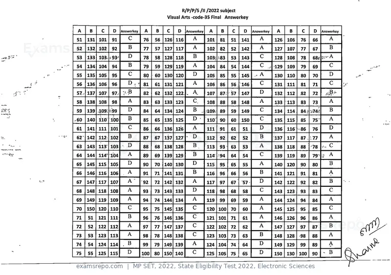
Text of page 34
R/P/P/S /II /2022 subject
                                               Visual Arts -code-35 Final Answerkey


 A     B    C     D    Answerkey    A    B     C   D     Answerkey    A     B    C    D     Answerkey   A      B     C     D    Answerkey

 51   131 101    91       c        76    56   126 116       A        101   81    51   141      A        126   106   76    66        A

 52   132 102    92       B        77    57   127 117       A        102   82    52   142      A        127   107   77    67       B

 53   133 103. ^93'       D        78    58   128 118       B        103^ -83    53   143      C        128   108   78    6Bs ?- A

 54   134 104    94       B        79    59   129 119       A        104   84    54   144      C , 129        109   79    69       C

 55   135 105    95       C        80    60   130 120       D        105   85    55   145      A        130   110   80    70       D

 56   136 106    96       D.. 81         61   131 121       A        106   86    56: 146       C        131   111   81    71       C
                                                                                                                    CO
 57. 137 107     97.               82    62   132 122.      A,       107   87. 57     147      D        132   112   82    72

 58   138 108    98       A        83    63   133 123       c.       108   88    58   148      A        133   113   83    73        A

 59   139 109:- e'99      D        84    64   134 124                :-109, 89   59   149      C        134   114                  B

.60   140 110    loo      B        85    65   135 125       D -      110   90    60   150      C        135   115   85    75"      A

 61   141 111 101         C        86    66   136 126       A        111   91    61   51       D        136   116   86    76       D

62~ 142 112: 102          B        87    67   137 127 -     D        112   92    62   52       B        137   117   87    -77      A

63    143 113 103         D        88    68   138 128       B        113   93    63   53       A        138   118   88    78    ., c

64    144 lie 104         A        89    69   139 129       B        lie   94    64   54       C        139   119   89    79    U' A
65    145 115    105      D        90    70   140 130       D        115   95    65   55       A        140   120   90    80       B

66    146 116 106         A        91    71   141 131       B        116   96    66   56       B        141   121   91    81       A

67    147 117    107      A"       92    72   142 132       A        117   97    67   57       D        142   122   92    82       B

68    148 118    108      A        93    73   143 133       D        118   98    68   58       C        143   123   93    83       C

69    149 119 109         A        94    74   144 134       A        119   99    69   59       A        144   124   94    84       A

70    150 120 110         C        95    75   145 135       C        120 100     70   60       A        145   125   95    85       C

71    51   121   111      B        96    76   146 136       C        121   101   71   61       A        146   126   96    86       A

72    52   122 112        A        97    77   147 137       c        122 102     72   62       A        147   127   97    87       B

73    53   123 113        A        98    78   148 138       c        123 103     73   63       B        148   128   88    88       A

74    54   124 114        B        99    79   149 139       A        124 104     74   64       D        149   129   99    89       A

75    55   125   115      D        100   80   150 140       C        125   105   75   65       D        150   130   100   90    - B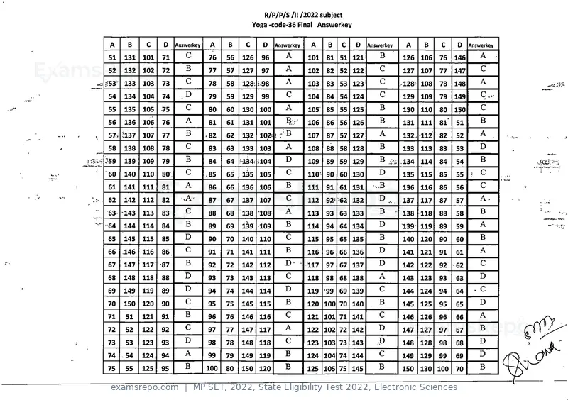
Text of page 35
R/P/P/S /II /2022 subject
                                                      Yoga -code-36 Final Answerkey


 A      B      C    D     Answerkey    A    B     C      D     Answerkey    A      B   C     D    Answerkey     A      B     C    D     Answerkey

 51    131-   101   71       c        76    56   126    96        A        101    81 51 121           B        126    106   76    146        A     .

 52    132    102   72       B        77    57   127    97        A        102    82 52 122           C        127    107   77    147        C

i;53- 133     103   73       C        78    58   128'. ■3S        A        103    83   53   123       C        128- 108     78    148        A

 54    134    104   74                79    59   129    99        C        104    84   54 124         C        129    109   79    149        c,..

 55    135    105   .75      C        80    60   130    100       A        105    85   55   125       B        130    110   80    150        C

 56    136    106   76       A        81    61   131 101                   106    86   56 126         B        131    111   81"   51         B

 57. il37     107   77       B        82    62   132    102;
                                                               j v' B      107    87   57 127         A        132.. 112    82    52         A

 58    138    108   78     ' C        83    63   133    103       A        108    88   58   128       B        133    113   83    53         D

:^59   139    109   79       B        84    64   -134. ilOA       D        109    89   59 129                  .134   114   84    54         B

 60    140    110   SO;      C        .85   65   135    105       C        110    90   60 .130        D        135    115   85    55    :    C

 61    141    111   81       A        86    66   136    106       B        111    91 61 131        -..B        136    116   86    56         C

 62    142    112   82     -.A-       87    67   137    107       C        112    92^ 62 132          D^       137    117   87    57         A,.

 63^ '143     113   83       C        88    68   138    108       A        113    93   63   133       B       V 138   118   88    58         B

-64    144    114   84       B        89    69   139 >109         B        114    94   64 134        D         139    119   89    59         A

 65    145    115   85       D        90    70   140    110       C        115    95   65   135       B        140    120   90    60         B

 66    146    116   86.      C        91    71   141 111          B        116    96   66 136        D         141    121   91    61         A

 67    147    117   87       B        92    72   142    112       D"       -117   97   67 137        D         142    122   92    62         C

 68    148    118   88       D        93    73   143    113       C        118    98   68 138         A        143    123   93    63         D

 69    149    119   89       D        94    74   144    114       D        119 •99     69 139         C        144    124   94    64        . C

 70    150    120   90       C        95    75   145    115       B        120 100 70 140             B        145    125   95    65         D

 71     51    121   91       B        96    76   146    116       C        121 101 71 141             C        146    126   96    66         A

 72     52    122   92       C        97    77   147   117        A        122 102 72 142            D         147    127   97    67         B

 73     53    123   93       D        98    78   148   118        C        123 103 73       143      .'P       148    128   98    68         D

 74    .54    124   94       A        99    79   149   119        B        124 104 74 144             C        149    129   99    69         D

 75    55     125   95       B        100   80   150   120        B        125    105 75 145         B         150    130   100   70         B
Page 1 of 40
Source: Madhya Pradesh Public Service Commission. Question paper published by Madhya Pradesh Public Service Commission.