
MH SET 2021: 26 September, Paper II, Electronic Science
Text of page 1
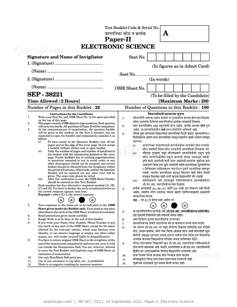
Test Booklet Code & Serial No.
                                                                                                                     A
                                                ELECTRONIC SCIENCE
Signature and Name of Invigilator                                                          Seat No.
1. (Signature) .........................................
                                                                                                           (In figures as in Admit Card)
      (Name) ................................................
                                                                                  Seat No. ..............................................................
2. (Signature) .........................................                                              (In words)
      (Name) ................................................                 OMR Sheet No.
SEP - 38221                                                                                         (To be filled by the Candidate)
Time Allowed : 2 Hours]                                                                                 [Maximum Marks : 200
Number of Pages in this Booklet : 32                                                     Number of Questions in this Booklet : 100
                      Instructions for the Candidates
1.         Write your Seat No. and OMR Sheet No. in the space provided              1.
           on the top of this page.
2.         This paper consists of 100 objective type questions. Each question
           will carry two marks. All questions of Paper II will be compulsory.      2.
3.         At the commencement of examination, the question booklet
           will be given to the student. In the first 5 minutes, you are            3.
           requested to open the booklet and compulsorily examine it as
           follows :
           (i)      To have access to the Question Booklet, tear off the
                    paper seal on the edge of this cover page. Do not accept                (i)
                    a booklet without sticker-seal or open booklet.
           (ii)     Tally the number of pages and number of questions in
                    the booklet with the information printed on the cover                   (ii)
                    page. Faulty booklets due to missing pages/questions
                    or questions repeated or not in serial order or any
                    other discrepancy should not be accepted and correct
                    booklet should be obtained from the invigilator within
                    the period of 5 minutes. Afterwards, neither the Question
                    Booklet will be replaced nor any extra time will be
                    given. The same may please be noted.
           (iii)    After this verification is over, the OMR Sheet Number
                                                                                            (iii)
                    should be entered on this Test Booklet.
4.         Each question has four alternative responses marked (A), (B),
           (C) and (D). You have to darken the circle as indicated below on         4.                     (A), (B), (C)    (D)
           the correct response against each item.
           Example : where (C) is the correct response.

                              A        B                 D                                           (C)
5.         Your responses to the items are to be indicated in the OMR                                      A        B               D
           Sheet given inside the Booklet only. If you mark at any place
           other than in the circle in the OMR Sheet, it will not be evaluated.     5.
6.         Read instructions given inside carefully.
7.         Rough Work is to be done at the end of this booklet.                     6.
8.         If you write your Name, Seat Number, Phone Number or put                 7.
           any mark on any part of the OMR Sheet, except for the space
                                                                                    8.
           allotted for the relevant entries, which may disclose your
           identity, or use abusive language or employ any other unfair
           means, you will render yourself liable to disqualification.
9.         You have to return original OMR Sheet to the invigilator at the
           end of the examination compulsorily and must not carry it with           9.
           you outside the Examination Hall. You are, however, allowed
           to carry the Test Booklet and duplicate copy of OMR Sheet on
           conclusion of examination.
                                                                                    10.
10.        Use only Blue/Black Ball point pen.
                                                                                    11.
11.        Use of any calculator or log table, etc., is prohibited.
12.        There is no negative marking for incorrect answers.                      12.
Text of page 2
SEP - 38221/II—A


2
Text of page 3
SEP - 38221/II—A
                            Electronic Science
                                     Paper II
Time Allowed : 120 Minutes]                          [Maximum Marks : 200
Note : This Paper contains Hundred (100) multiple choice questions. Each question
       carrying Two (2) marks. Attempt All questions.

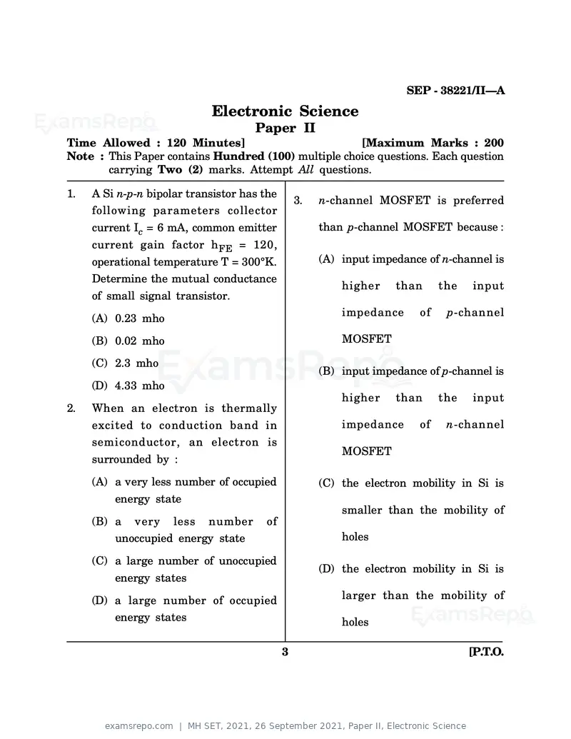
1.   A Si n-p-n bipolar transistor has the
                                                 3.   n-channel MOSFET is preferred
     following parameters collector
     current Ic = 6 mA, common emitter                than p-channel MOSFET because :
     current gain factor h FE = 120,
     operational temperature T = 300°K.               (A) input impedance of n-channel is
     Determine the mutual conductance
                                                          higher    than      the   input
     of small signal transistor.
                                                          impedance      of    p-channel
     (A) 0.23 mho

     (B) 0.02 mho                                         MOSFET

     (C) 2.3 mho
                                                      (B) input impedance of p-channel is
     (D) 4.33 mho
                                                          higher    than      the   input
2.   When an electron is thermally
     excited to conduction band in                        impedance      of    n-channel
     semiconductor, an electron is
                                                          MOSFET
     surrounded by :

     (A) a very less number of occupied               (C) the electron mobility in Si is
         energy state
                                                          smaller than the mobility of
     (B) a   very    less   number     of
         unoccupied energy state                          holes

     (C) a large number of unoccupied
                                                      (D) the electron mobility in Si is
         energy states

     (D) a large number of occupied                       larger than the mobility of
         energy states                                    holes

                                             3                                      [P.T.O.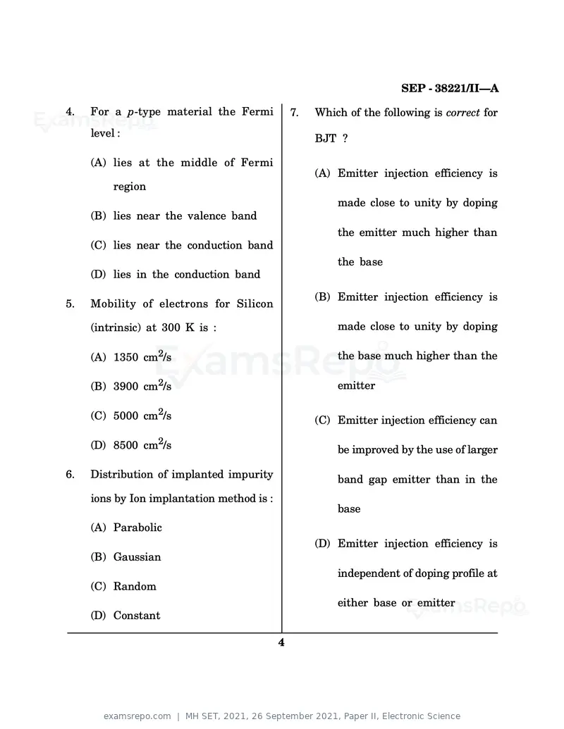
Text of page 4
SEP - 38221/II—A

4.   For a p-type material the Fermi            7.   Which of the following is correct for
     level :                                         BJT ?

     (A) lies at the middle of Fermi
                                                     (A) Emitter injection efficiency is
          region
                                                         made close to unity by doping
     (B) lies near the valence band
                                                         the emitter much higher than
     (C) lies near the conduction band
                                                         the base
     (D) lies in the conduction band

                                                     (B) Emitter injection efficiency is
5.   Mobility of electrons for Silicon

     (intrinsic) at 300 K is :                           made close to unity by doping

     (A) 1350 cm2/s                                      the base much higher than the

     (B) 3900 cm2/s                                      emitter

     (C) 5000 cm2/s                                  (C) Emitter injection efficiency can

     (D) 8500 cm2/s                                      be improved by the use of larger

6.   Distribution of implanted impurity                  band gap emitter than in the
     ions by Ion implantation method is :
                                                         base
     (A) Parabolic
                                                     (D) Emitter injection efficiency is
     (B) Gaussian
                                                         independent of doping profile at
     (C) Random
                                                         either base or emitter
     (D) Constant

                                            4
Text of page 5
SEP - 38221/II—A

8.   Typical    value     of    impurity         10. Match List I with List II and select

     concentration in a Tunnel diode is :            the correct answer using the codes
                                                     given below :

     (A) 1 part in 1010 parts                                          List I

                                                     (a) Donor energy band
     (B) 1 part in 108 parts
                                                     (b) Fermi           level         of     p-type
                                                           semiconductor                at     room
     (C) 1 part in 106 parts                               temperature

                                                     (c)   Acceptor energy band
     (D) 1 part in 103 parts
                                                     (d) Fermi          level      in       intrinsic
                                                           semiconductor
9.   A Zener diode when used in voltage
                                                                   List II
     stabilisation circuits is biased in :           (1) At the middle of the forbidden
                                                           energy gap
     (A) Reverse-bias region below the
                                                     (2) Close to the conduction band

         breakdown voltage                           (3) Very close to the valence band

                                                     (4) Close to the valence band
     (B) Reverse-breakdown region                    Codes :

                                                           (a)   (b)     (c)     (d)
     (C) Forward-biased region
                                                     (A) (4)     (3)     (2)     (1)

     (D) Forward      biased    constant             (B) (2)     (1)     (4)     (3)

                                                     (C) (4)     (1)     (2)     (3)
         current mode
                                                     (D) (2)     (3)     (4)     (1)

                                             5                                                [P.T.O.
Text of page 6
SEP - 38221/II—A

11. In the circuit shown in the figure,         13. Consider the following energy
    the power dissipated in 30   resistor           storage capability of basic passive

    will be maximum, if the value of R              elements is due to the fact that :

    is :                                            (1) Resistance dissipitates energy

                                                    (2) Capacitor stores energy

                                                    (3) Inductor dissipates energy

                                                    Which of the above is/are correct ?

                                                    (A) (1), (2) and (3)

                                                    (B) (1) and (2)

                                                    (C) (3) alone

                                                    (D) (1) and (3)
    (A) 30
                                                14. FIR filters are :

    (B) 16                                          (A) Recursive where present output
                                                        depends on present and past
    (C) 9                                               inputs and output samples only

    (D) Zero                                        (B) Non-recursive where present
                                                        output depends on present and
12. A network has 10 nodes and 17
                                                        past input samples only
    branches. The number of different
                                                    (C) Recursive where present output
    node pair voltages would be :
                                                        depends on present and past
    (A) 7                                               input samples only

    (B) 17                                          (D) Non-recursive where present
                                                        output depends on present and
    (C) 45
                                                        past inputs and output samples
    (D) 50
                                                        only
                                            6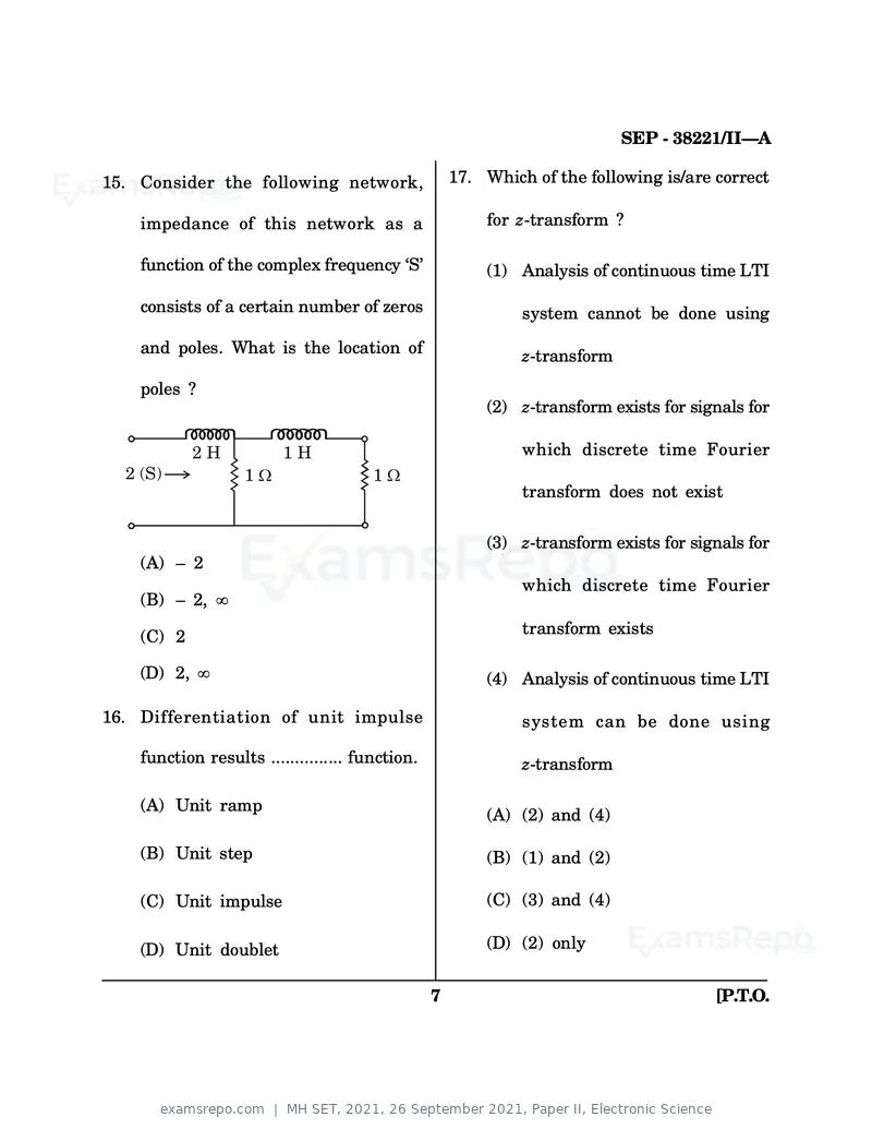
Text of page 7
SEP - 38221/II—A

15. Consider the following network,                  17. Which of the following is/are correct

    impedance of this network as a                       for z-transform ?

    function of the complex frequency ‘S’                (1) Analysis of continuous time LTI

    consists of a certain number of zeros                     system cannot be done using

    and poles. What is the location of                        z-transform
    poles ?
                                                         (2) z-transform exists for signals for

                                                              which discrete time Fourier

                                                              transform does not exist

                                                         (3) z-transform exists for signals for
    (A) – 2
                                                              which discrete time Fourier
    (B) – 2,

    (C) 2                                                     transform exists

    (D) 2,                                               (4) Analysis of continuous time LTI

16. Differentiation of unit impulse                           system can be done using

    function results ............... function.                z-transform

    (A) Unit ramp
                                                         (A) (2) and (4)

    (B) Unit step                                        (B) (1) and (2)

    (C) Unit impulse                                     (C) (3) and (4)

    (D) Unit doublet                                     (D) (2) only


                                                 7                                     [P.T.O.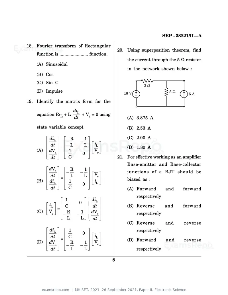
Text of page 8
SEP - 38221/II—A

18. Fourier transform of Rectangular
                                                        20. Using superposition theorem, find
    function is ....................... function.
                                                            the current through the 5    resistor
    (A) Sinusoidal
                                                            in the network shown below :
    (B) Cos
    (C) Sin C
    (D) Impulse

19. Identify the matrix form for the

                           diL
    equation RiL + L           + Vc = 0 using
                           dt                               (A) 3.875 A

    state variable concept.                                 (B) 2.53 A

           diL           R         1                        (C) 2.00 A
            dt           L         L    iL
                                                            (D) 1.80 A
    (A)    dVc          1               Vc
                                  0
            dt          C                               21. For effective working as an amplifier
                                                            Base-emitter and Base-collector
           dVc           R         1
                                                            junctions of a BJT should be
            dt           L         L    Vc
    (B)    diL          1               iL                  biased as :
                                  0
            dt          C                                   (A) Forward          and    forward
                                                                 respectively
                      1                diL
            iL                0
                      C                 dt                  (B) Reverse          and    forward
    (C)    Vc          R       1       dVc                       respectively
                       L       L       dt
                                                            (C) Reverse          and    reverse
            diL         1                                        respectively
                                  0
            dt          C               iL
    (D)                                 Vc                  (D) Forward          and    reverse
           dVc           R         1
            dt           L         L                             respectively

                                                    8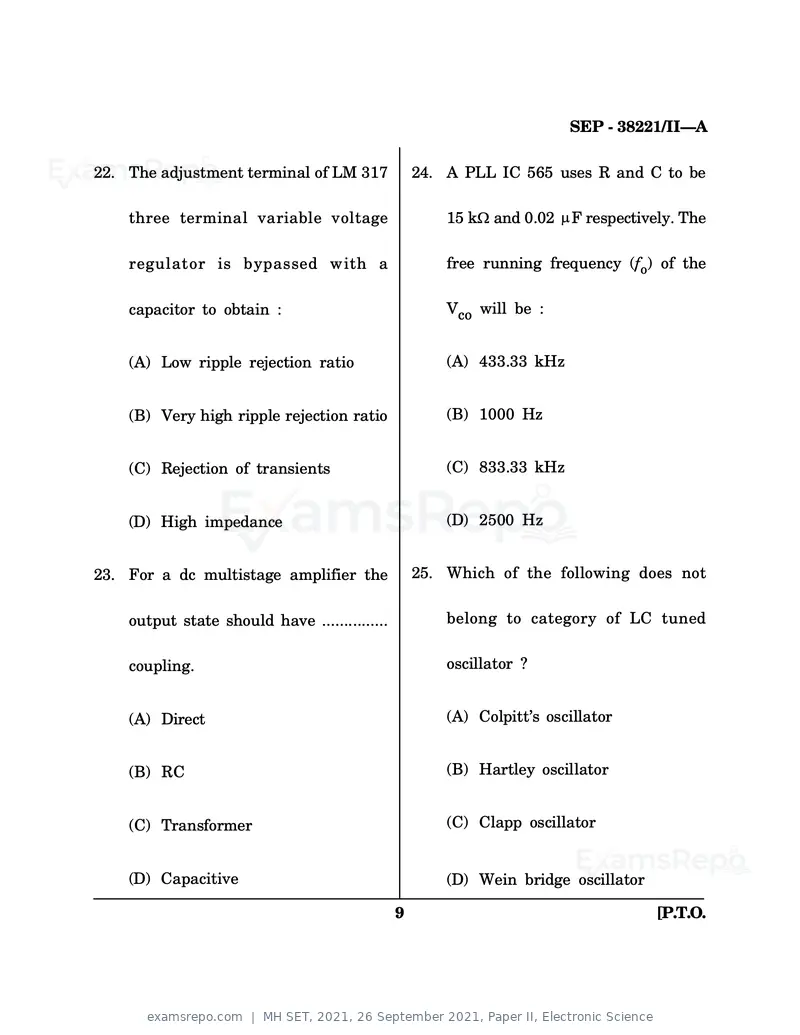
Text of page 9
SEP - 38221/II—A

22. The adjustment terminal of LM 317              24. A PLL IC 565 uses R and C to be

    three terminal variable voltage                    15 k   and 0.02   F respectively. The

    regulator is bypassed with a                       free running frequency (fo) of the

    capacitor to obtain :                              Vco will be :


    (A) Low ripple rejection ratio                     (A) 433.33 kHz


    (B) Very high ripple rejection ratio               (B) 1000 Hz


    (C) Rejection of transients                        (C) 833.33 kHz


    (D) High impedance                                 (D) 2500 Hz


23. For a dc multistage amplifier the              25. Which of the following does not


    output state should have ...............           belong to category of LC tuned


    coupling.                                          oscillator ?


    (A) Direct                                         (A) Colpitt’s oscillator


    (B) RC                                             (B) Hartley oscillator


    (C) Transformer                                    (C) Clapp oscillator


    (D) Capacitive                                     (D) Wein bridge oscillator

                                               9                                     [P.T.O.
Text of page 10
SEP - 38221/II—A


26. An op-amp based comparator with               28. Identify the correct sequence of the


     positive feedback is called :                    following with increasing value of


                                                      gain :
     (A) Astable multivibrator

                                                      (i)   Amplifier without feedback
     (B) Schmitt trigger

                                                      (ii) Amplifier with positive feedback
     (C) Pulse generator

                                                      (iii) Oscillator
     (D) Integrator
                                                      (iv) Amplifier         with      negative

27. The roll-off of a first order low pass
                                                            feedback

     filter is :
                                                      Codes :

     (A) +20 dB/decade
                                                      (A) (iv), (iii), (ii), (i)

     (B) –20 dB/decade
                                                      (B) (i),   (iii), (ii), (iv)

     (C) +40 dB/decade
                                                      (C) (iv), (i),     (ii), (iii)


     (D) –40 dB/decade                                (D) (i),   (ii), (iii), (iv)

                                             10
Text of page 11
SEP - 38221/II—A

29. Match List-I with List-II and select                30. Assertion (A) :

    the correct answer from the codes                       An operational amplifier should
    given below :                                           have a low input offset current.

                       List I                               Reason (R) :
    (a) Wein bridge oscillator
                                                            Input impedance of operational
    (b) Voltage            shunt        feedback
                                                            amplifier is very high.
          amplifier
                                                            (A) Both (A) and (R) are true and
    (c) Crystal oscillator
                                                                 (R) is correct explanation
    (d) Current            shunt        feedback
                                                                 of (A)
          amplifier
                                                            (B) Both (A) and (R) are true but
                    List II
                                                                 (R) is not correct explanation
    (i)   RF range
                                                                 of (A)
    (ii) AF range
                                                            (C) (A) is true and (R) is false
    (iii) Low output impedance
                                                            (D) (A) is false and (R) is true
    (iv) High output impedance
                                                        31. Multiplexer facilitates the following
    (v) Low input impedance
                                                            conversion :
    Codes :
                                                            (A) Single input to one of the
          (a)   (b)      (c)    (d)
                                                                 multiple outputs
    (A) (iii) (i)        (ii) (v)
                                                            (B) Multiple inputs to single output
    (B) (ii) (iii) (i)          (v)

    (C) (v)     (ii)     (i)    (iii)                       (C) Decimal to hexadecimal

    (D) (iv) (iii) (v)          (i)                         (D) Odd parity to even parity

                                                   11                                     [P.T.O.
Text of page 12
SEP - 38221/II—A

32. The minimum memory size to
                                             35. Reliable clock distribution is key to
    implement a BCD to seven segment
    decoder will be :                            synchronous operation of high speed
    (A) 16 bytes
                                                 digital circuits. The device used for
    (B) 10 bytes

    (C) 1 k bytes                                clock synchronisation in FPGA is :

    (D) 8 bytes
                                                 (A) DLL
33. Output frequency in the following

    diagram will be :
                                                 (B) CLB


                                                 (C) IOB


                                                 (D) JTAG
    (A) 1 kHz

    (B) 100 Hz                               36. Which one of the following is not a
    (C) 13 Hz
                                                 PLD ?
    (D) 8 Hz

34. A DFF is said to be transparent              (A) PLA
    when :

    (A) The output is LOW                        (B) CPLD

    (B) The output is HIGH
                                                 (C) SPROM
    (C) The output follows the clock

    (D) The output follows the input             (D) CLA

                                        12
Text of page 13
SEP - 38221/II—A

37. For 3 : 8 decoder, the LED will be            39. Match the List-I with List-II and

    switched on for :                                 select the correct answer using the

                                                      codes given below :

                                                                         List-I

                                                      (a) Flash ADC

                                                      (b) Dual slope ADC

                                                      (c)   Successive Approximation ADC

                                                      (d) DAC

    (A) C B A + C B A + C B A + C B A                                   List-II

    (B) C B A + C B A + C B A + C B A                 (i)   Music synthesiser


    (C) C B A + C B A + C B A + C B A                 (ii) DMM

                                                      (iii) Digital Camera
    (D) C B A + C B A + C B A + C B A
                                                      (iv) Speech digitisation
38. Propagation delay of logic families
                                                      Codes :
    in descending order can be listed as :
                                                            (a)   (b)      (c)     (d)
    (A) ECL, TTL, CMOS
                                                      (A) (iii) (iv) (i)           (ii)
    (B) TTL, ECL, CMOS
                                                      (B) (i)     (ii)     (iii) (iv)
    (C) CMOS, TTL, ECL
                                                      (C) (iii) (ii)       (iv) (i)

    (D) ECL, CMOS, TTL                                (D) (ii) (i)         (iv) (iii)

                                             13                                            [P.T.O.
Text of page 14
SEP - 38221/II—A

                                                 42. The register which acts as an
40. Assertion (A) :
                                                     operand and destination of result for
    2’s complement arithmetic is
                                                     arithmetic operations is ........... and the
    preferred in digital computers.
                                                     status of result is stored, is ..........
    Reason (R) :
                                                     (A) B, C
    The hardware required to obtain 2’s
                                                     (B) C, D
    complement of a number is simple.
                                                     (C) D, A
    (A) Both (A) and (R) are true and
        (R) is the correct explanation               (D) A, PSW

        of (A)                                   43. Advantage of segmented addressing
    (B) Both (A) and (R) are true but                is :
        (R)      is   not   the   correct
                                                     (A) Size of segment is fixed
        explanation of (A)
                                                     (B) Size of segment is variable
    (C) (A) is true but (R) is false
    (D) (A) is false and (R) is true                 (C) Used in pipelining

41. The Program Counter is a :                       (D) Supports DMA

    (A) 16-bit upcounter with parallel           44. The effective address, if segment

        load                                         register is 3000 and offset is 2020

                                                     will be :
    (B) 8-bit up/down counter
                                                     (A) 30002
    (C) 16-bit down counter with
        parallel load                                (B) 32020

                                                     (C) 05020
    (D) 16-bit Shift Register with
        parallel load                                (D) 23020

                                            14
Text of page 15
SEP - 38221/II—A

45. The 8086 is a ................. processor                 47. On power up, the 8051 uses

     with .............................. architecture.            following locations in the RAM for

     (A) 8 bit, Von Neumann                                       registers Ro – RI and bit addressable


     (B) 16 bit, Harvard                                          memory :


     (C) 16 bit, Pipelined                                        (A) 00 – 2F and 2F – 30


     (D) 16 bit, Von Neumann                                      (B) 00 – 7F and 7F – FF

46. The TH0 and TL0 registers of 8051
                                                                  (C) 00 – 07 and 20 – 2F

     are loaded with 05 H and has 1 MHz
                                                                  (D) 30 – 7F and 20 – 2F
     clock input in auto-reload mode, to
                                                              48. The correct sequence of steps for
     generate a square wave. The
                                                                  instruction execution is :
     frequency of the square wave will

                                                                  (A) Decode, opcode fetch and
     be approximately :

                                                                      execute
     (A) 1 kHz


     (B) 2 kHz                                                    (B) Execute, decode, opcode fetch


     (C) 50 kHz                                                   (C) Opcode fetch, decode, execute


     (D) 20 kHz                                                   (D) Decode, execute, opcode fetch

                                                         15                                    [P.T.O.
Text of page 16
SEP - 38221/II—A

49. Match List I with List II and select        50. Assertion (A) :
    the correct answer using the codes
                                                    IO/ M pin is used to access memory.
    given below :
                                                    Reason (R) :
                       List I
                                                    In memory mapped I/O the input/
    (a) Register addressing
                                                    output ports are accessed as
    (b) Immediate addressing                        memory.

    (c) Relative addressing                         (A) Both (A) and (R) are true and

    (d) Indexed addressing                              (R) is the correct explanation

                                                        of (A)
                   List II
                                                    (B) Both (A) and (R) are true but
    (i)   MOVC A, @ A + PC
                                                        (R) is not correct explanation
    (ii) DJNZ R2, LOOP
                                                        of (A)
    (iii) MOV A, # 55H
                                                    (C) (A) is true but (R) is false
    (iv) MOV A, R1
                                                    (D) (A) is false but (R) is true
    Codes :
                                                51. Which is the final step in wafer
          (a)   (b)      (c)    (d)                 processing sequence ?

    (A) (i)     (ii)     (iii) (iv)                 (A) Photolithography

    (B) (iv) (iii) (ii) (i)                         (B) Chemical vapor

    (C) (iii) (ii)       (iv) (i)                   (C) Metallization

    (D) (iv) (iii) (i)          (ii)                (D) Oxidation

                                           16
Text of page 17
SEP - 38221/II—A

52. When the input of the CMOS                54. Match List I with List II and select
    inverter is equal to ‘Inverter
    Threshold Voltage’ V th , the                 the correct answer using the codes
    transistors are operating in :                given below :
    (A) N-MOS is cut-off, P-MOS is in
                                                                    List I
        saturation
                                                  (a) Very          low       static   power
    (B) P-MOS is cut-off, n-MOS is in
        saturation                                      consumption
    (C) Both the transistors are in               (b) Image data storage
        linear region
                                                  (c)   Reducing device dimensions
    (D) Both the transistors are in
        saturation region                         (d) Planning of layout
53. Assertion (A) :
                                                                List II
    CMOS inverter is more power
    efficient compared to regular                 (i)   Scaling
    resistor-MOSFET inverter.
                                                  (ii) Stick diagram
    Reason (R) :
                                                  (iii) CMOS
    The dynamic power consumption of
    a CMOS inverter increases with                (iv) CCD
    increasing switching frequency.
                                                  Codes :
    (A) Both (A) and (R) are true and
        (R) is the correct explanation                  (a)   (b)     (c)     (d)
        of (A)
                                                  (A) (i)     (iii) (ii) (iv)
    (B) Both (A) and (R) are true but
        (R) is not the correct                    (B) (iv) (ii)       (i)     (iii)
        explanation of (A)
                                                  (C) (i)     (iv) (ii) (iii)
    (C) (A) is true but (R) is false
                                                  (D) (iii) (iv) (i)          (ii)
    (D) (A) and (R) both are false

                                         17                                            [P.T.O.
Text of page 18
SEP - 38221/II—A

55. With help of Scanning Electron              58. Which one of the following is not an

    Microscope (SEM) one can resolve                advantage of CMOS technology over

    objects as small as :                           NMOS ?

                                                    (A) Very      low     static     power
    (A) 10 mm
                                                         consumption
    (B) 1 micron
                                                    (B) High density of logic functions
    (C) 10 nm                                            on a chip

    (D) 1 nm                                        (C) Less number of fabrication steps

56. Which of the following represents a             (D) High noise immunity

    transistor in stick diagram of
                                                59. IoT uses which of the following
    VLSIs ?

    (A) Black Crossing Blue                         modules in appropriate sequence :

    (B) Red Crossing Brown                          (A) Cloud storage, Data analysis,

                                                         Sensors, Data Acquisition
    (C) Red Crossing Green

    (D) Blue Crossing Green                         (B) Sensor, Data Acquisition,

                                                         Communication, Cloud storage
57. Drift velocity of       carriers in
    semiconductor device having electric            (C) Data      Acquisition,        Data
    field strength E is given by :                       analysis,      Cloud      storage,

    (A)   .E                                             Communication

    (B) E/                                          (D) Communication,                Data

    (C)   /E                                             Acquisition, Cloud storage,

    (D) 2.E                                              Sensor

                                           18
Text of page 19
SEP - 38221/II—A


60. Correlation of
                                                     62. High frequency resistance of an

    x (n) = (1, 2, 1) and y (n) = (1, 2, – 1)
                                                         antenna of length ‘l’, cross-section
    will be :

                                                         ‘A’, conductivity ‘ ’, perimeter ‘P’
    (A) {1, 4, 2, –4, 1}


    (B) {–1, 0, 4, 3, 1}                                 (   0 is free space permeability,      is


    (C) {1, 4, 2, 1, 4}
                                                         operating frequency) is given by :

    (D) {–1, 2, 4, –2, 1}

                                                                         0
                                                         (A) l/P                 ohms
                                                                     2
61. MST RADAR is used for :


    (A) Measuring speed of automobiles                   (B) l/2P                ohms
                                                                             0


    (B) Mapping the ground
                                                         (C) l/P             0

    (C) Searching         surface      non-

                                                                l        0
         uniformities                                    (D)
                                                               2     P

    (D) Finding attitude of cloud base

                                                19                                         [P.T.O.
Text of page 20
SEP - 38221/II—A

                                                 64. If the length of a linear dipole
63. Circular polarization of EM wave
                                                     antenna (l<< ), Ao is peak value of
    means electric and magnetic field
                                                     power density, r is radius, â is radial
    must have :
                                                     unit vector,         is usual spherical
    (A) Either electric or magnetic non-
                                                     co-ordinate, then the radiated power
        zero and positive propagation
                                                     density is given by :
        vector
                                                     (A) aˆ A 2o sin 2 /r2

    (B) Two       orthogonal      linear
                                                     (B) aˆ A o sin2 /r2
        components        with      real
                                                     (C) aˆ A o sin /r2
        magnitude and phase difference
                                                     (D) aˆ A 2o sin /r
        in even multiples of 90°
                                                 65. Electrical model of PIN diode in
    (C) Two       orthogonal      linear
                                                     microwave region can be given as
        components       with      same
                                                     below for forward bias :
        magnitude and phase difference
                                                     (A)
        in odd multiples of 90°
                                                     (B)
    (D) Both components non-zero and
                                                     (C)
        perpendicular to the direction of

        propagation                                  (D)

                                            20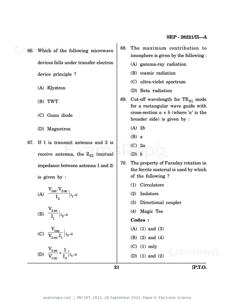
Text of page 21
SEP - 38221/II—A

                                                 68. The maximum contribution to
66. Which of the following microwave
                                                     ionosphere is given by the following :
    devices falls under transfer electron            (A) gamma-ray radiation

    device principle ?                               (B) cosmic radiation
                                                     (C) ultra-violet spectrum
    (A) Klystron
                                                     (D) Beta radiation

    (B) TWT                                      69. Cut-off wavelength for TE01 mode
                                                     for a ractangular wave guide with
                                                     cross-section a × b (where ‘a’ is the
    (C) Gunn diode
                                                     broader side) is given by :

    (D) Magnetron                                    (A) 2b
                                                     (B) a
67. If 1 is transmit antenna and 2 is
                                                     (C) 2a
    receive antenna, the Z21 (mutual                 (D) b
                                                 70. The property of Faraday rotation in
    impedance between antenna 1 and 2)
                                                     the ferrite material is used by which
    is given by :                                    of the following ?
                                                     (1) Circulators
          V1oc .V2 oc
    (A)                     I1 0                     (2) Isolators
                I2
                                                     (3) Directional coupler
          V2 oc
                                                     (4) Magic Tee
    (B)              I2 0
           I1
                                                     Codes :
         V1oc                                        (A) (1) and (3)
    (C) V .I I2 0
         2 oc 1                                      (B) (2) and (4)

          V2 oc                                      (C) (1) only
                      1
    (D) V             I2 I1 0                        (D) (1) and (2)
         1 oc


                                            21                                     [P.T.O.
Text of page 22
SEP - 38221/II—A

                                                73. Two frequencies 12 kHz and 14 kHz
71. Slope overload distortion in delta
                                                    sinusoidal in nature are added
    modulation can be reduced by :
                                                    together and given to the ideal

    (A) Decreasing sample rate                      frequency detector in demodulation.

                                                    The output of the detector is :
    (B) Decreasing the step size
                                                    (A) 12 kHz

    (C) Increasing the differential gain            (B) 2 kHz


    (D) Increasing the step size                    (C) 12 kHz and 14 kHz

                                                    (D) 14 kHz
72. A communication channel with
                                                74. An AM has carrier frequency and
    AWGN having SNR >>1 and
                                                    modulating signal frequency 2 MHz

    bandwidth B has capacity C1, if the             and   2    kHz     respectively.   An

                                                    appropriate value for the time
    SNR and bandwidth B is :
                                                    constant of the envelope detector in
    (A) C2 = C1 + 2B                                demodulator is :

                                                    (A) 0.08       s
    (B) C2 = 2 (C1 + B)

                                                    (B) 40     s
    (C) C2 = C1 + B
                                                    (C) 120        s

    (D) C2 = 4 (C1 + B)
                                                    (D) 0.10       s

                                           22
Text of page 23
SEP - 38221/II—A

75. In PSK modulator :                        76. For avoiding any alterations due to

                                                  gravity,     the   blood     pressure
    (a) QPSK utilizes four distinct
                                                  measurement is always done :
        levels of phase shift
                                                  (A) When the patient is on the

    (b) QPSK signal is equivalent to
                                                      move

        two BPSK signal, but with the
                                                  (B) When the patient is lying on bed

        carriers 90° out of phase with
                                                  (C) When the patient is standing

        one another
                                                  (D) On the right leg

    (c) QPSK utilizes four distinct           77. Data    sequence      ‘‘1101100001’’

        levels of amplitude and phase             transmitted at a speed of 1,00,000

        shift                                     bits/sec with a carrier frequency of

                                                  150 kHz corresponds to .................
    Options :
                                                  two-bit symbols/sec.

    (A) (a) and (c)
                                                  (A) 30,000

    (B) (a) and (b)
                                                  (B) 50,000

    (C) (c) only                                  (C) 1,00,000


    (D) (b) only                                  (D) 25,000

                                         23                                       [P.T.O.
Text of page 24
SEP - 38221/II—A

78. Match List I with List II and select        79. Capacity of communication channel
                                                    can be increased by :
    the correct answer using the codes
                                                    (a) Decreasing signal to noise ratio
    given below :
                                                    (b) Decreasing the bandwidth
                      List I
                                                    (c) Decreasing the noise in channel
    (a) TDM                                         (d) Increasing signal to noise ratio

    (b) FM                                          Codes :
                                                    (A) (a) and (d)
    (c) AM
                                                    (B) (b) and (c)
    (d) FDM
                                                    (C) (a) only (b)
                    List II                         (D) (c) and (d)
                                                80. Assertion (A) : Thermal noise
    (i)   Frequency detector
                                                    is sometimes referred to as white
    (ii) Envelope detector                          noise.
                                                    Reason (R) : When the white
    (iii) Sensitive to propagation delay            noise is passed through a network,
                                                    the spectral density will be altered
    (iv) Non-sensitive to propagation
                                                    by the shape of the network
          delay                                     frequency response.

    Codes :                                         (A) Both (A) and (R) are true and
                                                        (R) is the correct explanation
          (a)   (b)     (c)    (d)                      of (A)

    (A) (iii) (i)       (ii) (iv)                   (B) Both (A) and (R) are true but
                                                        (R) is not the correct
    (B) (iii) (ii)      (i)    (iv)                     explanation of (A)

    (C) (ii) (iii) (iv) (i)                         (C) (A) is true but (R) is false

    (D) (ii) (i)        (iv) (iii)                  (D) (A) is false and (R) is true

                                           24
Text of page 25
SEP - 38221/II—A

81. di/dt protection is provided to the          83. dv/dt protection is provided to the

    thyristor by :                                   SCR by :

    (A) Connecting an inductor in                    (A) Connecting a capacitor in

        parallel across the load                         parallel with the load


    (B) Connecting an inductor in                    (B) Connecting an inductor in

                                                         series with the load
        series with the load
                                                     (C) Connecting a capacitor and
    (C) Connecting an inductor in
                                                         resistor in parallel with the
        parallel across the gate terminal
                                                         device
    (D) Connecting an inductor in
                                                     (D) Connecting an inductor and
        series with the gate
                                                         resistor in parallel with the
82. The local hot spot formation in the
                                                         device
    cross-section    of    the   SCR   is
                                                 84. What is the absolute maximum
    avoided by :
                                                     operating/switching frequency of a
    (A) Reducing          the    junction            converter grade thyristor (SCR)
        temperature                                  whose turn-on and turn-off time are

                                                     3   s and 200    s respectively ?
    (B) Applying gate current nearer to

        the maximum gate current                     (A) 5.00 kHz

    (C) Using only R loads                           (B) 4.9 kHz

    (D) Proper mounting of the SCR on                (C) 10.0 kHz

        heat sink                                    (D) 20.0 kHz

                                            25                                    [P.T.O.
Text of page 26
SEP - 38221/II—A

85. Match the following :                 86. Lithium niobate is a combination of :

                       Set I
                                              (A) Electro-optic, piezo-electric and

    (a) Phase controlled converter                 optical properties

    (b) Chopper
                                              (B) Piezo-electric and optically

    (c) Inverter
                                                   active properties

    (d) Dimmerstat
                                              (C) Optical       and     mechanical
                      Set II
                                                   properties

    (i)   DC to DC conversion
                                              (D) Piezo-electric properties and
    (ii) DC to AC conversion
                                                   chemical properties
    (iii) AC to AC conversion
                                          87. Rayleigh      scattering      is   a
    (iv) AC to DC conversion
                                              fundamental loss mechanism arising
    Codes :
                                              from :
          (a)   (b)     (c)    (d)
                                              (A) Electrical fluctuations
    (A) (iv) (iii) (ii) (i)
                                              (B) Mechanical fluctuations
    (B) (iv) (i)        (ii) (iii)
                                              (C) Electronic fluctuations
    (C) (iv) (ii)       (iii) (i)

                                              (D) Local microscopic fluctuations
    (D) (i)     (ii)    (iii) (iv)
                                     26
Text of page 27
SEP - 38221/II—A

88. Silica fibres can change their optical        90. Match the pairs :

     properties permanently when they                                   Set I

     are exposed to :                                 (a) P-i-n diode

     (A) Electrical shocks                            (b) Optical flip-flop

     (B) High power electrostatic shock               (c)   Fibre laser Transmitter

                                                      (d) Grating
     (C) Intense radiation from a laser

         operating in blue/ultraviolet                                  Set II

         spectrum                                     (i)   WDM components


     (D) Intense radiation from a laser               (ii) Photodetector

         operating in a red and green                 (iii) High speed communication

         spectrum                                     (iv) Semiconductor                 laser   and

                                                            amplifier
89. The bandwidth of a photodetector is
                                                      Codes :
     defined as :

                                                            (a)   (b)     (c)     (d)
     (A) [2 ( tr    RC )] 1

                                                      (A) (ii) (iv) (iii) (i)
     (B) [2 ( tr    RC
                       )] 1
                                                      (B) (ii) (iv) (iii) (i)
     (C) 2 ( tr     RC )
                                                      (C) (iii) (ii)      (i)     (iv)
     (D) (2 ( tr    RC
                           ) 1) 1
                                                      (D) (iv) (iii) (ii) (i)

                                             27                                              [P.T.O.
Text of page 28
SEP - 38221/II—A

                                                 93. An integrator contains 100 k     and
91. MEMS       are   minitiarised      to
                                                     1 F capacitor. If the voltage applied

    microscopic level and therefore                  to the integrator is 1 Volt, what is
                                                     the output of the integrator after 1

    have :                                           sec ?

                                                     (A) 10 V

    (A) Low sensitivity                              (B) 5 V

                                                     (C) 15 V
    (B) Large dynamic range
                                                     (D) 0 V
                                                 94. If the time/div control is set to
    (C) Very low frequency response                  2 s/div, determine the frequency of
                                                     the wave form shown in figure
                                                     below :
    (D) High mechanical strength


92. What is the sensitivity of a 200   A


    meter movement for a DC voltmeter :


    (A) 10 k /V


    (B) 1 k /V

                                                     (A) 100 kHz
    (C) 5 k /V                                       (B) 50 kHz

                                                     (C) 150 kHz
    (D) 2.5 k /V
                                                     (D) 125 kHz
                                            28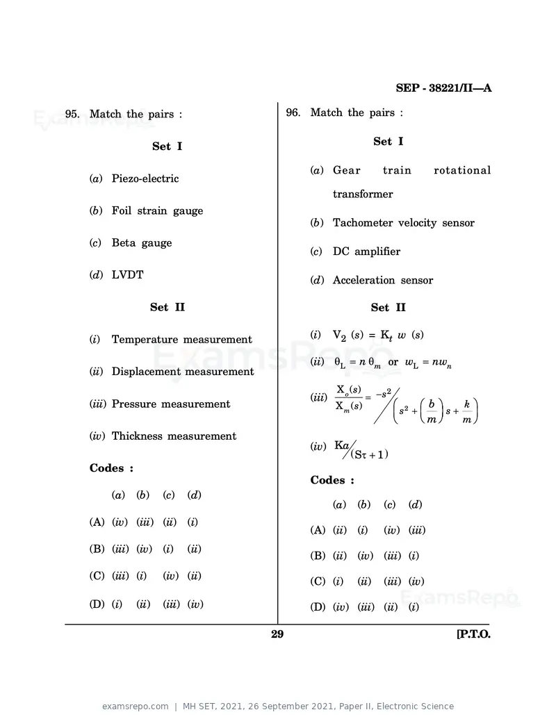
Text of page 29
SEP - 38221/II—A

95. Match the pairs :                      96. Match the pairs :


                       Set I                                        Set I

                                               (a) Gear                 train            rotational
    (a) Piezo-electric
                                                       transformer
    (b) Foil strain gauge
                                               (b) Tachometer velocity sensor
    (c) Beta gauge
                                               (c)     DC amplifier

    (d) LVDT                                   (d) Acceleration sensor

                      Set II                                       Set II

    (i)   Temperature measurement              (i)     V2 (s) = Kt w (s)

                                               (ii)     L     n     m    or wL           nwn
    (ii) Displacement measurement
                                                       X o ( s)         s2
                                               (iii)
    (iii) Pressure measurement                         X m ( s)                          b      k
                                                                              s2           s
                                                                                         m      m
    (iv) Thickness measurement
                                               (iv) Ka
                                                             S      1
    Codes :
                                               Codes :
          (a)   (b)     (c)    (d)
                                                       (a)   (b)        (c)        (d)
    (A) (iv) (iii) (ii) (i)
                                               (A) (ii) (i)             (iv) (iii)
    (B) (iii) (iv) (i)         (ii)
                                               (B) (ii) (iv) (iii) (i)
    (C) (iii) (i)       (iv) (ii)
                                               (C) (i)       (ii)       (iii) (iv)

    (D) (i)     (ii)    (iii) (iv)             (D) (iv) (iii) (ii) (i)

                                      29                                                       [P.T.O.
Text of page 30
SEP - 38221/II—A

97. A good control system has the                         99. The minimum number of states

    following features, except :
                                                              required to describe the two degree
    (A) Good stability
                                                              differential equation :
    (B) A simple system
                                                              (A) 1
    (C) Good accuracy

                                                              (B) 2
    (D) Sufficient power handling

98. The transfer function y(s)/Td(s) for                      (C) 3

    the following system (shown in fig)                       (D) 4

    is :
                                                          100. The transfer function y(s)/U(s) of

                                                              a system described by the state

                                                              equations dX/dt = –2 X + 24 and

                                                              y(t) = 0.5x is :
           y( s)                  G( s)
    (A) Td (s)     1
                        [1   G1 ( s) G 2 (s) H(s)]
                                                              (A) 0.5/(s – 2)
           y( s)
    (B) Td ( s)    0
                                                              (B) 1/(s – 2)
           y( s)             G( s)
    (C) Td (s)     [1   G1 (s) G 2 ( s) H(s)]                 (C) 0.5/(s + 2)

           y( s)             G( s)
    (D) Td (s)                                                (D) 1/(s + 2)
                   [1   G1 (s) G 2 ( s) H( s)]

                                                     30
Text of page 31
SEP - 38221/II—A

ROUGH WORK


    31                 [P.T.O.
Text of page 32
SEP - 38221/II—A

ROUGH WORK


    32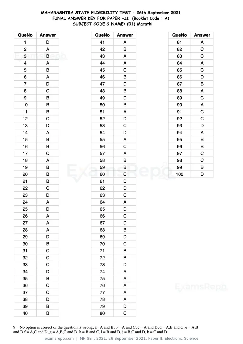
Text of page 1
MAHARASHTRA STATE ELIGIBILITY TEST - 26th September 2021
                    FINAL ANSWER KEY FOR PAPER -II (Booklet Code : A)
                            SUBJECT CODE & NAME: (01) Marathi

  QueNo        Answer                            QueNo        Answer                           QueNo        Answer
      1            D                               41             A                               81              A
      2            A                               42             B                               82              C
      3            B                               43             A                               83              C
      4            A                               44             A                               84              A
      5            B                               45             C                               85              C
      6            A                               46             B                               86              D
      7            D                               47             D                               87              B
      8            C                               48             B                               88              A
      9            B                               49             D                               89              C
     10            B                               50             B                               90              A
     11            B                               51             A                               91              C
     12            C                               52             D                               92              C
     13            D                               53             C                               93              D
     14            A                               54             D                               94              A
     15            B                               55             A                               95              B
     16            B                               56             C                               96              B
     17            C                               57             A                               97              C
     18            A                               58             B                               98              C
     19            B                               59             B                               99              B
     20            B                               60             C                              100              D
     21            B                               61             D
     22            C                               62             D
     23            D                               63             C
     24            A                               64             A
     25            D                               65             D
     26            A                               66             C
     27            A                               67             D
     28            A                               68             B
     29            D                               69             D
     30            B                               70             C
     31            C                               71             B
     32            C                               72             B
     33            C                               73             D
     34            D                               74             A
     35            B                               75             A
     36            C                               76             A
     37            C                               77             A
     38            D                               78             A
     39            B                               79             D
     40            B                               80             C


9 = No option is correct or the question is wrong, a= A and B, b = A and C, c = A and D, d = A,B and C, e = A,B
and D,f = A,C and D, g = A,B,C and D, h = B and C, i = B and D, j = B,C and D, k = C and D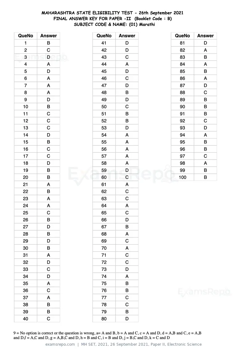
Text of page 2
MAHARASHTRA STATE ELIGIBILITY TEST - 26th September 2021
                    FINAL ANSWER KEY FOR PAPER -II (Booklet Code : B)
                            SUBJECT CODE & NAME: (01) Marathi

  QueNo        Answer                            QueNo        Answer                           QueNo        Answer
      1            B                               41             D                               81              D
      2            C                               42             D                               82              A
      3            D                               43             C                               83              B
      4            A                               44             A                               84              A
      5            D                               45             D                               85              B
      6            A                               46             C                               86              A
      7            A                               47             D                               87              D
      8            A                               48             B                               88              C
      9            D                               49             D                               89              B
     10            B                               50             C                               90              B
     11            C                               51             B                               91              B
     12            C                               52             B                               92              C
     13            C                               53             D                               93              D
     14            D                               54             A                               94              A
     15            B                               55             A                               95              B
     16            C                               56             A                               96              B
     17            C                               57             A                               97              C
     18            D                               58             A                               98              A
     19            B                               59             D                               99              B
     20            B                               60             C                              100              B
     21            A                               61             A
     22            B                               62             C
     23            A                               63             C
     24            A                               64             A
     25            C                               65             C
     26            B                               66             D
     27            D                               67             B
     28            B                               68             A
     29            D                               69             C
     30            B                               70             A
     31            A                               71             C
     32            D                               72             C
     33            C                               73             D
     34            D                               74             A
     35            A                               75             B
     36            C                               76             B
     37            A                               77             C
     38            B                               78             C
     39            B                               79             B
     40            C                               80             D


9 = No option is correct or the question is wrong, a= A and B, b = A and C, c = A and D, d = A,B and C, e = A,B
and D,f = A,C and D, g = A,B,C and D, h = B and C, i = B and D, j = B,C and D, k = C and D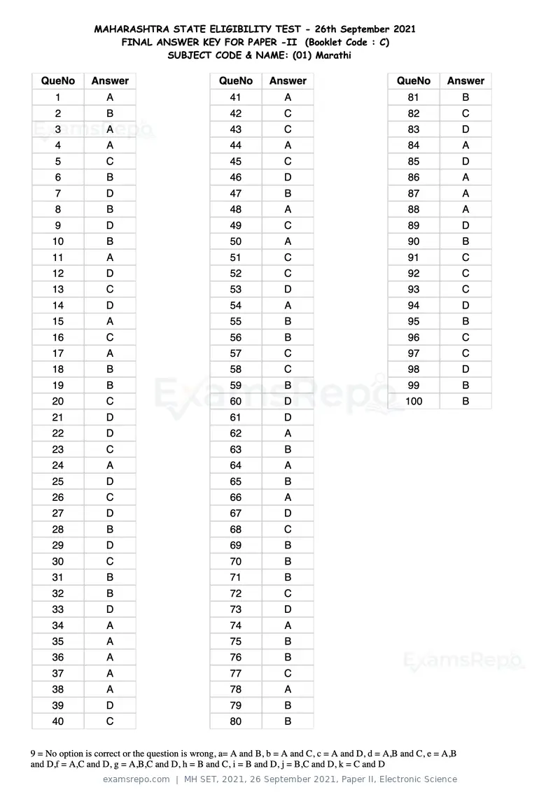
Text of page 3
MAHARASHTRA STATE ELIGIBILITY TEST - 26th September 2021
                    FINAL ANSWER KEY FOR PAPER -II (Booklet Code : C)
                            SUBJECT CODE & NAME: (01) Marathi

  QueNo        Answer                            QueNo        Answer                           QueNo        Answer
      1            A                               41             A                               81              B
      2            B                               42             C                               82              C
      3            A                               43             C                               83              D
      4            A                               44             A                               84              A
      5            C                               45             C                               85              D
      6            B                               46             D                               86              A
      7            D                               47             B                               87              A
      8            B                               48             A                               88              A
      9            D                               49             C                               89              D
     10            B                               50             A                               90              B
     11            A                               51             C                               91              C
     12            D                               52             C                               92              C
     13            C                               53             D                               93              C
     14            D                               54             A                               94              D
     15            A                               55             B                               95              B
     16            C                               56             B                               96              C
     17            A                               57             C                               97              C
     18            B                               58             C                               98              D
     19            B                               59             B                               99              B
     20            C                               60             D                              100              B
     21            D                               61             D
     22            D                               62             A
     23            C                               63             B
     24            A                               64             A
     25            D                               65             B
     26            C                               66             A
     27            D                               67             D
     28            B                               68             C
     29            D                               69             B
     30            C                               70             B
     31            B                               71             B
     32            B                               72             C
     33            D                               73             D
     34            A                               74             A
     35            A                               75             B
     36            A                               76             B
     37            A                               77             C
     38            A                               78             A
     39            D                               79             B
     40            C                               80             B


9 = No option is correct or the question is wrong, a= A and B, b = A and C, c = A and D, d = A,B and C, e = A,B
and D,f = A,C and D, g = A,B,C and D, h = B and C, i = B and D, j = B,C and D, k = C and D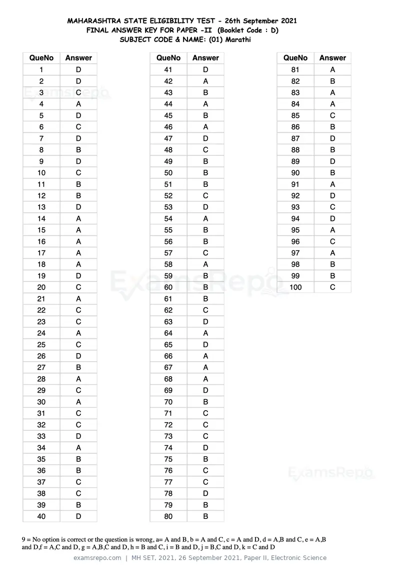
Text of page 4
MAHARASHTRA STATE ELIGIBILITY TEST - 26th September 2021
                    FINAL ANSWER KEY FOR PAPER -II (Booklet Code : D)
                            SUBJECT CODE & NAME: (01) Marathi

  QueNo        Answer                            QueNo        Answer                           QueNo        Answer
      1            D                               41             D                               81              A
      2            D                               42             A                               82              B
      3            C                               43             B                               83              A
      4            A                               44             A                               84              A
      5            D                               45             B                               85              C
      6            C                               46             A                               86              B
      7            D                               47             D                               87              D
      8            B                               48             C                               88              B
      9            D                               49             B                               89              D
     10            C                               50             B                               90              B
     11            B                               51             B                               91              A
     12            B                               52             C                               92              D
     13            D                               53             D                               93              C
     14            A                               54             A                               94              D
     15            A                               55             B                               95              A
     16            A                               56             B                               96              C
     17            A                               57             C                               97              A
     18            A                               58             A                               98              B
     19            D                               59             B                               99              B
     20            C                               60             B                              100              C
     21            A                               61             B
     22            C                               62             C
     23            C                               63             D
     24            A                               64             A
     25            C                               65             D
     26            D                               66             A
     27            B                               67             A
     28            A                               68             A
     29            C                               69             D
     30            A                               70             B
     31            C                               71             C
     32            C                               72             C
     33            D                               73             C
     34            A                               74             D
     35            B                               75             B
     36            B                               76             C
     37            C                               77             C
     38            C                               78             D
     39            B                               79             B
     40            D                               80             B


9 = No option is correct or the question is wrong, a= A and B, b = A and C, c = A and D, d = A,B and C, e = A,B
and D,f = A,C and D, g = A,B,C and D, h = B and C, i = B and D, j = B,C and D, k = C and D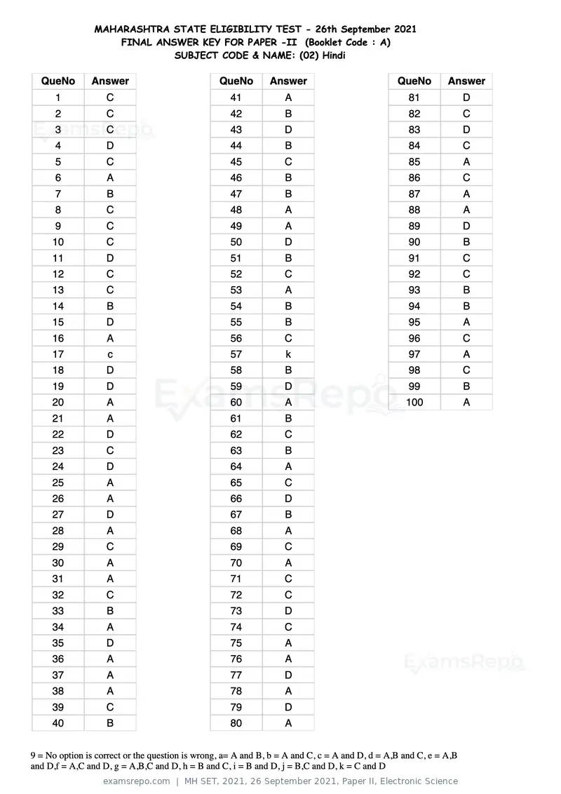
Text of page 5
MAHARASHTRA STATE ELIGIBILITY TEST - 26th September 2021
                    FINAL ANSWER KEY FOR PAPER -II (Booklet Code : A)
                             SUBJECT CODE & NAME: (02) Hindi

  QueNo        Answer                            QueNo        Answer                           QueNo        Answer
      1            C                               41             A                               81              D
      2            C                               42             B                               82              C
      3            C                               43             D                               83              D
      4            D                               44             B                               84              C
      5            C                               45             C                               85              A
      6            A                               46             B                               86              C
      7            B                               47             B                               87              A
      8            C                               48             A                               88              A
      9            C                               49             A                               89              D
     10            C                               50             D                               90              B
     11            D                               51             B                               91              C
     12            C                               52             C                               92              C
     13            C                               53             A                               93              B
     14            B                               54             B                               94              B
     15            D                               55             B                               95              A
     16            A                               56             C                               96              C
     17             c                              57             k                               97              A
     18            D                               58             B                               98              C
     19            D                               59             D                               99              B
     20            A                               60             A                              100              A
     21            A                               61             B
     22            D                               62             C
     23            C                               63             B
     24            D                               64             A
     25            A                               65             C
     26            A                               66             D
     27            D                               67             B
     28            A                               68             A
     29            C                               69             C
     30            A                               70             A
     31            A                               71             C
     32            C                               72             C
     33            B                               73             D
     34            A                               74             C
     35            D                               75             A
     36            A                               76             A
     37            A                               77             D
     38            A                               78             A
     39            C                               79             D
     40            B                               80             A


9 = No option is correct or the question is wrong, a= A and B, b = A and C, c = A and D, d = A,B and C, e = A,B
and D,f = A,C and D, g = A,B,C and D, h = B and C, i = B and D, j = B,C and D, k = C and D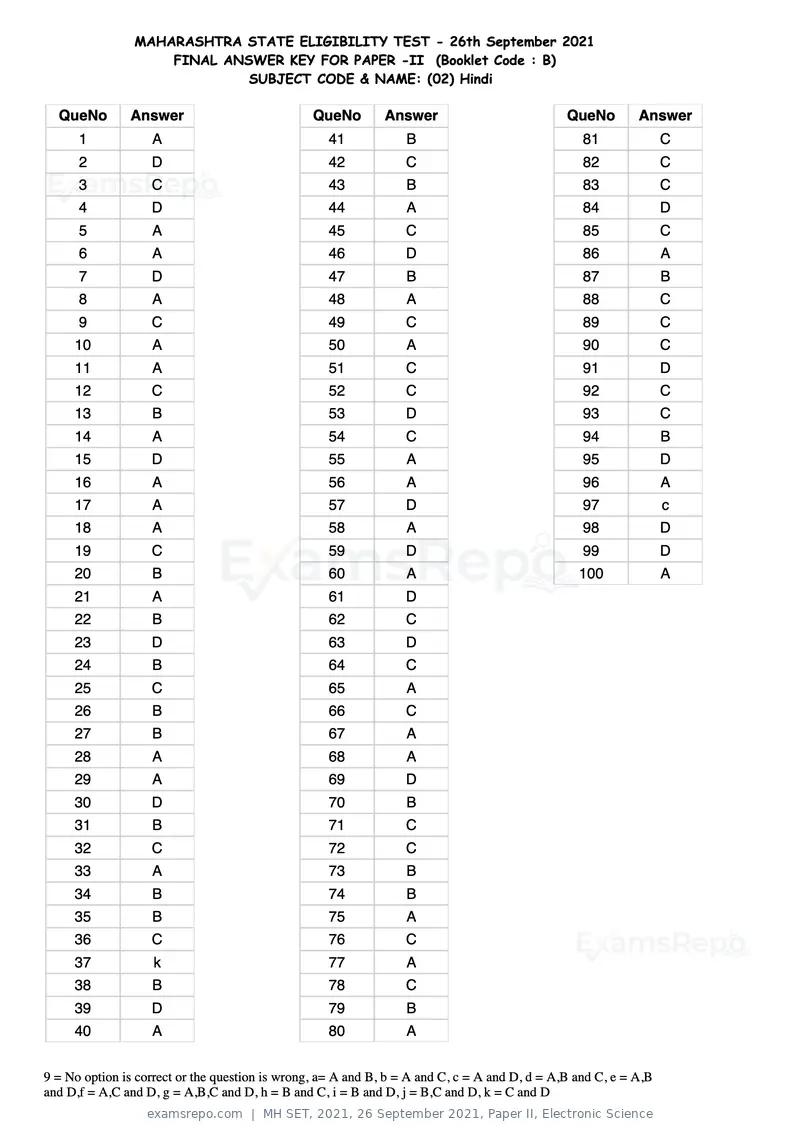
Text of page 6
MAHARASHTRA STATE ELIGIBILITY TEST - 26th September 2021
                    FINAL ANSWER KEY FOR PAPER -II (Booklet Code : B)
                             SUBJECT CODE & NAME: (02) Hindi

  QueNo        Answer                            QueNo        Answer                           QueNo        Answer
      1            A                               41             B                               81              C
      2            D                               42             C                               82              C
      3            C                               43             B                               83              C
      4            D                               44             A                               84              D
      5            A                               45             C                               85              C
      6            A                               46             D                               86              A
      7            D                               47             B                               87              B
      8            A                               48             A                               88              C
      9            C                               49             C                               89              C
     10            A                               50             A                               90              C
     11            A                               51             C                               91              D
     12            C                               52             C                               92              C
     13            B                               53             D                               93              C
     14            A                               54             C                               94              B
     15            D                               55             A                               95              D
     16            A                               56             A                               96              A
     17            A                               57             D                               97              c
     18            A                               58             A                               98              D
     19            C                               59             D                               99              D
     20            B                               60             A                              100              A
     21            A                               61             D
     22            B                               62             C
     23            D                               63             D
     24            B                               64             C
     25            C                               65             A
     26            B                               66             C
     27            B                               67             A
     28            A                               68             A
     29            A                               69             D
     30            D                               70             B
     31            B                               71             C
     32            C                               72             C
     33            A                               73             B
     34            B                               74             B
     35            B                               75             A
     36            C                               76             C
     37             k                              77             A
     38            B                               78             C
     39            D                               79             B
     40            A                               80             A


9 = No option is correct or the question is wrong, a= A and B, b = A and C, c = A and D, d = A,B and C, e = A,B
and D,f = A,C and D, g = A,B,C and D, h = B and C, i = B and D, j = B,C and D, k = C and D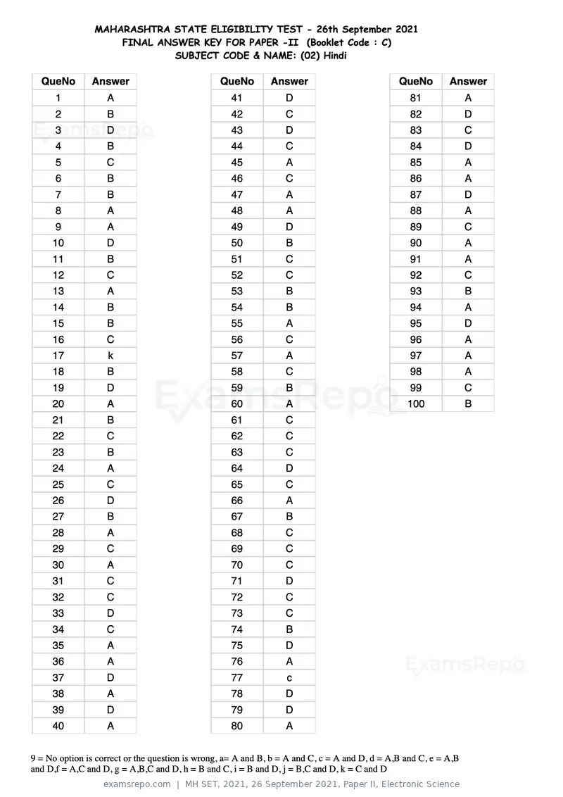
Text of page 7
MAHARASHTRA STATE ELIGIBILITY TEST - 26th September 2021
                    FINAL ANSWER KEY FOR PAPER -II (Booklet Code : C)
                             SUBJECT CODE & NAME: (02) Hindi

  QueNo        Answer                            QueNo        Answer                           QueNo        Answer
      1            A                               41             D                               81              A
      2            B                               42             C                               82              D
      3            D                               43             D                               83              C
      4            B                               44             C                               84              D
      5            C                               45             A                               85              A
      6            B                               46             C                               86              A
      7            B                               47             A                               87              D
      8            A                               48             A                               88              A
      9            A                               49             D                               89              C
     10            D                               50             B                               90              A
     11            B                               51             C                               91              A
     12            C                               52             C                               92              C
     13            A                               53             B                               93              B
     14            B                               54             B                               94              A
     15            B                               55             A                               95              D
     16            C                               56             C                               96              A
     17             k                              57             A                               97              A
     18            B                               58             C                               98              A
     19            D                               59             B                               99              C
     20            A                               60             A                              100              B
     21            B                               61             C
     22            C                               62             C
     23            B                               63             C
     24            A                               64             D
     25            C                               65             C
     26            D                               66             A
     27            B                               67             B
     28            A                               68             C
     29            C                               69             C
     30            A                               70             C
     31            C                               71             D
     32            C                               72             C
     33            D                               73             C
     34            C                               74             B
     35            A                               75             D
     36            A                               76             A
     37            D                               77             c
     38            A                               78             D
     39            D                               79             D
     40            A                               80             A


9 = No option is correct or the question is wrong, a= A and B, b = A and C, c = A and D, d = A,B and C, e = A,B
and D,f = A,C and D, g = A,B,C and D, h = B and C, i = B and D, j = B,C and D, k = C and D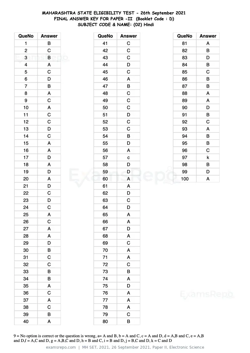
Text of page 8
MAHARASHTRA STATE ELIGIBILITY TEST - 26th September 2021
                    FINAL ANSWER KEY FOR PAPER -II (Booklet Code : D)
                             SUBJECT CODE & NAME: (02) Hindi

  QueNo        Answer                            QueNo        Answer                           QueNo        Answer
      1            B                               41             C                               81              A
      2            C                               42             C                               82              B
      3            B                               43             C                               83              D
      4            A                               44             D                               84              B
      5            C                               45             C                               85              C
      6            D                               46             A                               86              B
      7            B                               47             B                               87              B
      8            A                               48             C                               88              A
      9            C                               49             C                               89              A
     10            A                               50             C                               90              D
     11            C                               51             D                               91              B
     12            C                               52             C                               92              C
     13            D                               53             C                               93              A
     14            C                               54             B                               94              B
     15            A                               55             D                               95              B
     16            A                               56             A                               96              C
     17            D                               57             c                               97              k
     18            A                               58             D                               98              B
     19            D                               59             D                               99              D
     20            A                               60             A                              100              A
     21            D                               61             A
     22            C                               62             D
     23            D                               63             C
     24            C                               64             D
     25            A                               65             A
     26            C                               66             A
     27            A                               67             D
     28            A                               68             A
     29            D                               69             C
     30            B                               70             A
     31            C                               71             A
     32            C                               72             C
     33            B                               73             B
     34            B                               74             A
     35            A                               75             D
     36            C                               76             A
     37            A                               77             A
     38            C                               78             A
     39            B                               79             C
     40            A                               80             B


9 = No option is correct or the question is wrong, a= A and B, b = A and C, c = A and D, d = A,B and C, e = A,B
and D,f = A,C and D, g = A,B,C and D, h = B and C, i = B and D, j = B,C and D, k = C and D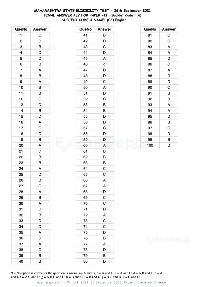
Text of page 9
MAHARASHTRA STATE ELIGIBILITY TEST - 26th September 2021
                    FINAL ANSWER KEY FOR PAPER -II (Booklet Code : A)
                            SUBJECT CODE & NAME: (03) English

  QueNo        Answer                            QueNo        Answer                           QueNo        Answer
      1            C                               41             B                               81              C
      2            D                               42             D                               82              C
      3            B                               43             C                               83              A
      4            D                               44             D                               84              A
      5            D                               45             A                               85              D
      6            B                               46             g                               86              C
      7            A                               47             D                               87              A
      8            B                               48             D                               88              D
      9            A                               49             C                               89              D
     10            B                               50             A                               90              C
     11            B                               51             D                               91              B
     12            C                               52             C                               92              B
     13            D                               53             B                               93              A
     14            B                               54             B                               94              A
     15            D                               55             D                               95              D
     16            A                               56             D                               96              B
     17            C                               57             C                               97              C
     18            C                               58             D                               98              D
     19            B                               59             D                               99              B
     20            A                               60             A                              100              D
     21            D                               61             B
     22            B                               62             B
     23            B                               63             B
     24            A                               64             C
     25            D                               65             C
     26            B                               66             A
     27            C                               67             A
     28            A                               68             D
     29            B                               69             C
     30            A                               70             C
     31            D                               71             D
     32            B                               72             A
     33            D                               73             C
     34            D                               74             C
     35            A                               75             D
     36            D                               76             B
     37            A                               77             A
     38            C                               78             D
     39            B                               79             B
     40            B                               80             D


9 = No option is correct or the question is wrong, a= A and B, b = A and C, c = A and D, d = A,B and C, e = A,B
and D,f = A,C and D, g = A,B,C and D, h = B and C, i = B and D, j = B,C and D, k = C and D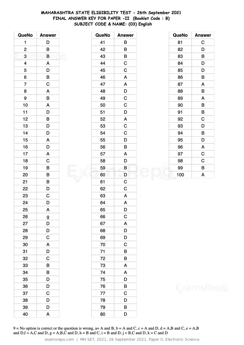
Text of page 10
MAHARASHTRA STATE ELIGIBILITY TEST - 26th September 2021
                    FINAL ANSWER KEY FOR PAPER -II (Booklet Code : B)
                            SUBJECT CODE & NAME: (03) English

  QueNo        Answer                            QueNo        Answer                           QueNo        Answer
      1            D                               41             B                               81              C
      2            B                               42             B                               82              D
      3            B                               43             B                               83              B
      4            A                               44             C                               84              D
      5            D                               45             C                               85              D
      6            B                               46             A                               86              B
      7            C                               47             A                               87              A
      8            A                               48             D                               88              B
      9            B                               49             C                               89              A
     10            A                               50             C                               90              B
     11            D                               51             D                               91              B
     12            B                               52             A                               92              C
     13            D                               53             C                               93              D
     14            D                               54             C                               94              B
     15            A                               55             D                               95              D
     16            D                               56             B                               96              A
     17            A                               57             A                               97              C
     18            C                               58             D                               98              C
     19            B                               59             B                               99              B
     20            B                               60             D                              100              A
     21            B                               61             C
     22            D                               62             C
     23            C                               63             A
     24            D                               64             A
     25            A                               65             D
     26            g                               66             C
     27            D                               67             A
     28            D                               68             D
     29            C                               69             D
     30            A                               70             C
     31            D                               71             B
     32            C                               72             B
     33            B                               73             A
     34            B                               74             A
     35            D                               75             D
     36            D                               76             B
     37            C                               77             C
     38            D                               78             D
     39            D                               79             B
     40            A                               80             D


9 = No option is correct or the question is wrong, a= A and B, b = A and C, c = A and D, d = A,B and C, e = A,B
and D,f = A,C and D, g = A,B,C and D, h = B and C, i = B and D, j = B,C and D, k = C and D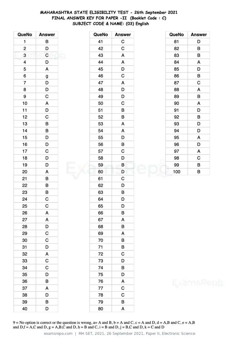
Text of page 11
MAHARASHTRA STATE ELIGIBILITY TEST - 26th September 2021
                    FINAL ANSWER KEY FOR PAPER -II (Booklet Code : C)
                            SUBJECT CODE & NAME: (03) English

  QueNo        Answer                            QueNo        Answer                           QueNo        Answer
      1            B                               41             C                               81              D
      2            D                               42             C                               82              B
      3            C                               43             A                               83              B
      4            D                               44             A                               84              A
      5            A                               45             D                               85              D
      6            g                               46             C                               86              B
      7            D                               47             A                               87              C
      8            D                               48             D                               88              A
      9            C                               49             D                               89              B
     10            A                               50             C                               90              A
     11            D                               51             B                               91              D
     12            C                               52             B                               92              B
     13            B                               53             A                               93              D
     14            B                               54             A                               94              D
     15            D                               55             D                               95              A
     16            D                               56             B                               96              D
     17            C                               57             C                               97              A
     18            D                               58             D                               98              C
     19            D                               59             B                               99              B
     20            A                               60             D                              100              B
     21            B                               61             C
     22            B                               62             D
     23            B                               63             B
     24            C                               64             D
     25            C                               65             D
     26            A                               66             B
     27            A                               67             A
     28            D                               68             B
     29            C                               69             A
     30            C                               70             B
     31            D                               71             B
     32            A                               72             C
     33            C                               73             D
     34            C                               74             B
     35            D                               75             D
     36            B                               76             A
     37            A                               77             C
     38            D                               78             C
     39            B                               79             B
     40            D                               80             A


9 = No option is correct or the question is wrong, a= A and B, b = A and C, c = A and D, d = A,B and C, e = A,B
and D,f = A,C and D, g = A,B,C and D, h = B and C, i = B and D, j = B,C and D, k = C and D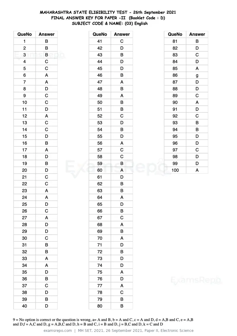
Text of page 12
MAHARASHTRA STATE ELIGIBILITY TEST - 26th September 2021
                    FINAL ANSWER KEY FOR PAPER -II (Booklet Code : D)
                            SUBJECT CODE & NAME: (03) English

  QueNo        Answer                            QueNo        Answer                           QueNo        Answer
      1            B                               41             C                               81              B
      2            B                               42             D                               82              D
      3            B                               43             B                               83              C
      4            C                               44             D                               84              D
      5            C                               45             D                               85              A
      6            A                               46             B                               86              g
      7            A                               47             A                               87              D
      8            D                               48             B                               88              D
      9            C                               49             A                               89              C
     10            C                               50             B                               90              A
     11            D                               51             B                               91              D
     12            A                               52             C                               92              C
     13            C                               53             D                               93              B
     14            C                               54             B                               94              B
     15            D                               55             D                               95              D
     16            B                               56             A                               96              D
     17            A                               57             C                               97              C
     18            D                               58             C                               98              D
     19            B                               59             B                               99              D
     20            D                               60             A                              100              A
     21            C                               61             D
     22            C                               62             B
     23            A                               63             B
     24            A                               64             A
     25            D                               65             D
     26            C                               66             B
     27            A                               67             C
     28            D                               68             A
     29            D                               69             B
     30            C                               70             A
     31            B                               71             D
     32            B                               72             B
     33            A                               73             D
     34            A                               74             D
     35            D                               75             A
     36            B                               76             D
     37            C                               77             A
     38            D                               78             C
     39            B                               79             B
     40            D                               80             B


9 = No option is correct or the question is wrong, a= A and B, b = A and C, c = A and D, d = A,B and C, e = A,B
and D,f = A,C and D, g = A,B,C and D, h = B and C, i = B and D, j = B,C and D, k = C and D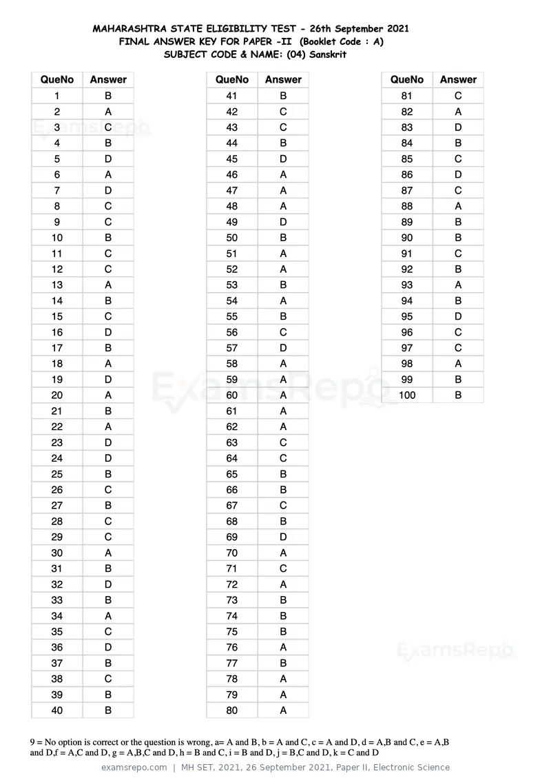
Text of page 13
MAHARASHTRA STATE ELIGIBILITY TEST - 26th September 2021
                    FINAL ANSWER KEY FOR PAPER -II (Booklet Code : A)
                            SUBJECT CODE & NAME: (04) Sanskrit

  QueNo        Answer                            QueNo        Answer                           QueNo        Answer
      1            B                               41             B                               81              C
      2            A                               42             C                               82              A
      3            C                               43             C                               83              D
      4            B                               44             B                               84              B
      5            D                               45             D                               85              C
      6            A                               46             A                               86              D
      7            D                               47             A                               87              C
      8            C                               48             A                               88              A
      9            C                               49             D                               89              B
     10            B                               50             B                               90              B
     11            C                               51             A                               91              C
     12            C                               52             A                               92              B
     13            A                               53             B                               93              A
     14            B                               54             A                               94              B
     15            C                               55             B                               95              D
     16            D                               56             C                               96              C
     17            B                               57             D                               97              C
     18            A                               58             A                               98              A
     19            D                               59             A                               99              B
     20            A                               60             A                              100              B
     21            B                               61             A
     22            A                               62             A
     23            D                               63             C
     24            D                               64             C
     25            B                               65             B
     26            C                               66             B
     27            B                               67             C
     28            C                               68             B
     29            C                               69             D
     30            A                               70             A
     31            B                               71             C
     32            D                               72             A
     33            B                               73             B
     34            A                               74             B
     35            C                               75             B
     36            D                               76             A
     37            B                               77             B
     38            C                               78             A
     39            B                               79             A
     40            B                               80             A


9 = No option is correct or the question is wrong, a= A and B, b = A and C, c = A and D, d = A,B and C, e = A,B
and D,f = A,C and D, g = A,B,C and D, h = B and C, i = B and D, j = B,C and D, k = C and D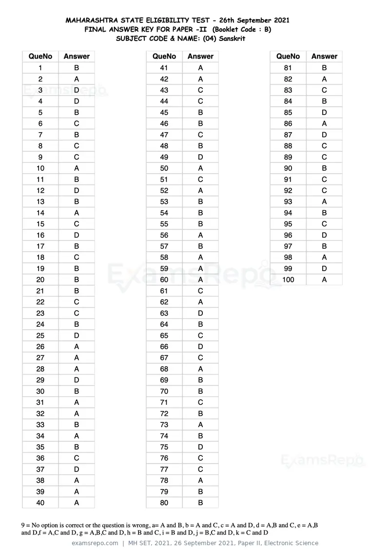
Text of page 14
MAHARASHTRA STATE ELIGIBILITY TEST - 26th September 2021
                    FINAL ANSWER KEY FOR PAPER -II (Booklet Code : B)
                           SUBJECT CODE & NAME: (04) Sanskrit

  QueNo        Answer                            QueNo        Answer                           QueNo        Answer
      1            B                               41             A                               81              B
      2            A                               42             A                               82              A
      3            D                               43             C                               83              C
      4            D                               44             C                               84              B
      5            B                               45             B                               85              D
      6            C                               46             B                               86              A
      7            B                               47             C                               87              D
      8            C                               48             B                               88              C
      9            C                               49             D                               89              C
     10            A                               50             A                               90              B
     11            B                               51             C                               91              C
     12            D                               52             A                               92              C
     13            B                               53             B                               93              A
     14            A                               54             B                               94              B
     15            C                               55             B                               95              C
     16            D                               56             A                               96              D
     17            B                               57             B                               97              B
     18            C                               58             A                               98              A
     19            B                               59             A                               99              D
     20            B                               60             A                              100              A
     21            B                               61             C
     22            C                               62             A
     23            C                               63             D
     24            B                               64             B
     25            D                               65             C
     26            A                               66             D
     27            A                               67             C
     28            A                               68             A
     29            D                               69             B
     30            B                               70             B
     31            A                               71             C
     32            A                               72             B
     33            B                               73             A
     34            A                               74             B
     35            B                               75             D
     36            C                               76             C
     37            D                               77             C
     38            A                               78             A
     39            A                               79             B
     40            A                               80             B


9 = No option is correct or the question is wrong, a= A and B, b = A and C, c = A and D, d = A,B and C, e = A,B
and D,f = A,C and D, g = A,B,C and D, h = B and C, i = B and D, j = B,C and D, k = C and D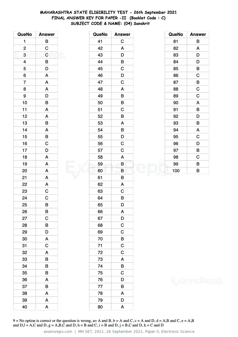
Text of page 15
MAHARASHTRA STATE ELIGIBILITY TEST - 26th September 2021
                    FINAL ANSWER KEY FOR PAPER -II (Booklet Code : C)
                           SUBJECT CODE & NAME: (04) Sanskrit

  QueNo        Answer                            QueNo        Answer                           QueNo        Answer
      1            B                               41             C                               81              B
      2            C                               42             A                               82              A
      3            C                               43             D                               83              D
      4            B                               44             B                               84              D
      5            D                               45             C                               85              B
      6            A                               46             D                               86              C
      7            A                               47             C                               87              B
      8            A                               48             A                               88              C
      9            D                               49             B                               89              C
     10            B                               50             B                               90              A
     11            A                               51             C                               91              B
     12            A                               52             B                               92              D
     13            B                               53             A                               93              B
     14            A                               54             B                               94              A
     15            B                               55             D                               95              C
     16            C                               56             C                               96              D
     17            D                               57             C                               97              B
     18            A                               58             A                               98              C
     19            A                               59             B                               99              B
     20            A                               60             B                              100              B
     21            A                               61             B
     22            A                               62             A
     23            C                               63             C
     24            C                               64             B
     25            B                               65             D
     26            B                               66             A
     27            C                               67             D
     28            B                               68             C
     29            D                               69             C
     30            A                               70             B
     31            C                               71             C
     32            A                               72             C
     33            B                               73             A
     34            B                               74             B
     35            B                               75             C
     36            A                               76             D
     37            B                               77             B
     38            A                               78             A
     39            A                               79             D
     40            A                               80             A


9 = No option is correct or the question is wrong, a= A and B, b = A and C, c = A and D, d = A,B and C, e = A,B
and D,f = A,C and D, g = A,B,C and D, h = B and C, i = B and D, j = B,C and D, k = C and D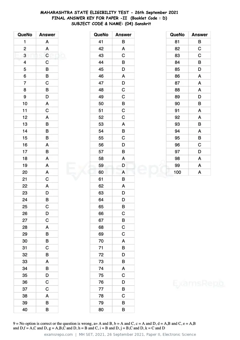
Text of page 16
MAHARASHTRA STATE ELIGIBILITY TEST - 26th September 2021
                    FINAL ANSWER KEY FOR PAPER -II (Booklet Code : D)
                            SUBJECT CODE & NAME: (04) Sanskrit

  QueNo        Answer                            QueNo        Answer                           QueNo        Answer
      1            A                               41             B                               81              B
      2            A                               42             A                               82              C
      3            C                               43             C                               83              C
      4            C                               44             B                               84              B
      5            B                               45             D                               85              D
      6            B                               46             A                               86              A
      7            C                               47             D                               87              A
      8            B                               48             C                               88              A
      9            D                               49             C                               89              D
     10            A                               50             B                               90              B
     11            C                               51             C                               91              A
     12            A                               52             C                               92              A
     13            B                               53             A                               93              B
     14            B                               54             B                               94              A
     15            B                               55             C                               95              B
     16            A                               56             D                               96              C
     17            B                               57             B                               97              D
     18            A                               58             A                               98              A
     19            A                               59             D                               99              A
     20            A                               60             A                              100              A
     21            C                               61             B
     22            A                               62             A
     23            D                               63             D
     24            B                               64             D
     25            C                               65             B
     26            D                               66             C
     27            C                               67             B
     28            A                               68             C
     29            B                               69             C
     30            B                               70             A
     31            C                               71             B
     32            B                               72             D
     33            A                               73             B
     34            B                               74             A
     35            D                               75             C
     36            C                               76             D
     37            C                               77             B
     38            A                               78             C
     39            B                               79             B
     40            B                               80             B


9 = No option is correct or the question is wrong, a= A and B, b = A and C, c = A and D, d = A,B and C, e = A,B
and D,f = A,C and D, g = A,B,C and D, h = B and C, i = B and D, j = B,C and D, k = C and D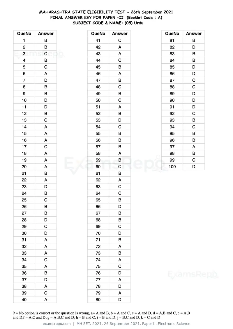
Text of page 17
MAHARASHTRA STATE ELIGIBILITY TEST - 26th September 2021
                    FINAL ANSWER KEY FOR PAPER -II (Booklet Code : A)
                             SUBJECT CODE & NAME: (05) Urdu

  QueNo        Answer                            QueNo        Answer                           QueNo        Answer
      1            B                               41             C                               81              B
      2            B                               42             A                               82              D
      3            C                               43             A                               83              B
      4            B                               44             C                               84              B
      5            C                               45             B                               85              D
      6            A                               46             A                               86              D
      7            D                               47             B                               87              C
      8            B                               48             C                               88              C
      9            B                               49             B                               89              D
     10            D                               50             C                               90              D
     11            D                               51             A                               91              D
     12            B                               52             B                               92              C
     13            C                               53             D                               93              B
     14            A                               54             C                               94              C
     15            A                               55             B                               95              B
     16            A                               56             B                               96              B
     17            C                               57             B                               97              A
     18            A                               58             A                               98              B
     19            A                               59             B                               99              C
     20            A                               60             C                              100              D
     21            B                               61             B
     22            A                               62             A
     23            D                               63             C
     24            B                               64             C
     25            C                               65             B
     26            B                               66             D
     27            B                               67             B
     28            D                               68             B
     29            C                               69             C
     30            D                               70             D
     31            A                               71             B
     32            A                               72             A
     33            A                               73             B
     34            C                               74             A
     35            A                               75             C
     36            B                               76             D
     37            D                               77             A
     38            A                               78             D
     39            C                               79             A
     40            A                               80             D


9 = No option is correct or the question is wrong, a= A and B, b = A and C, c = A and D, d = A,B and C, e = A,B
and D,f = A,C and D, g = A,B,C and D, h = B and C, i = B and D, j = B,C and D, k = C and D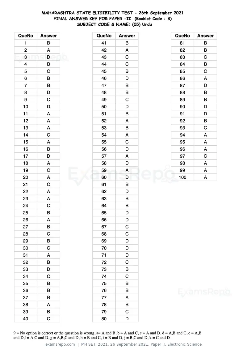
Text of page 18
MAHARASHTRA STATE ELIGIBILITY TEST - 26th September 2021
                    FINAL ANSWER KEY FOR PAPER -II (Booklet Code : B)
                             SUBJECT CODE & NAME: (05) Urdu

  QueNo        Answer                            QueNo        Answer                           QueNo        Answer
      1            B                               41             B                               81              B
      2            A                               42             A                               82              B
      3            D                               43             C                               83              C
      4            B                               44             C                               84              B
      5            C                               45             B                               85              C
      6            B                               46             D                               86              A
      7            B                               47             B                               87              D
      8            D                               48             B                               88              B
      9            C                               49             C                               89              B
     10            D                               50             D                               90              D
     11            A                               51             B                               91              D
     12            A                               52             A                               92              B
     13            A                               53             B                               93              C
     14            C                               54             A                               94              A
     15            A                               55             C                               95              A
     16            B                               56             D                               96              A
     17            D                               57             A                               97              C
     18            A                               58             D                               98              A
     19            C                               59             A                               99              A
     20            A                               60             D                              100              A
     21            C                               61             B
     22            A                               62             D
     23            A                               63             B
     24            C                               64             B
     25            B                               65             D
     26            A                               66             D
     27            B                               67             C
     28            C                               68             C
     29            B                               69             D
     30            C                               70             D
     31            A                               71             D
     32            B                               72             C
     33            D                               73             B
     34            C                               74             C
     35            B                               75             B
     36            B                               76             B
     37            B                               77             A
     38            A                               78             B
     39            B                               79             C
     40            C                               80             D


9 = No option is correct or the question is wrong, a= A and B, b = A and C, c = A and D, d = A,B and C, e = A,B
and D,f = A,C and D, g = A,B,C and D, h = B and C, i = B and D, j = B,C and D, k = C and D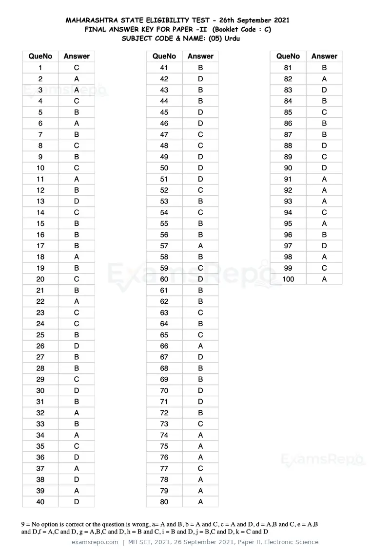
Text of page 19
MAHARASHTRA STATE ELIGIBILITY TEST - 26th September 2021
                    FINAL ANSWER KEY FOR PAPER -II (Booklet Code : C)
                             SUBJECT CODE & NAME: (05) Urdu

  QueNo        Answer                            QueNo        Answer                           QueNo        Answer
      1            C                               41             B                               81              B
      2            A                               42             D                               82              A
      3            A                               43             B                               83              D
      4            C                               44             B                               84              B
      5            B                               45             D                               85              C
      6            A                               46             D                               86              B
      7            B                               47             C                               87              B
      8            C                               48             C                               88              D
      9            B                               49             D                               89              C
     10            C                               50             D                               90              D
     11            A                               51             D                               91              A
     12            B                               52             C                               92              A
     13            D                               53             B                               93              A
     14            C                               54             C                               94              C
     15            B                               55             B                               95              A
     16            B                               56             B                               96              B
     17            B                               57             A                               97              D
     18            A                               58             B                               98              A
     19            B                               59             C                               99              C
     20            C                               60             D                              100              A
     21            B                               61             B
     22            A                               62             B
     23            C                               63             C
     24            C                               64             B
     25            B                               65             C
     26            D                               66             A
     27            B                               67             D
     28            B                               68             B
     29            C                               69             B
     30            D                               70             D
     31            B                               71             D
     32            A                               72             B
     33            B                               73             C
     34            A                               74             A
     35            C                               75             A
     36            D                               76             A
     37            A                               77             C
     38            D                               78             A
     39            A                               79             A
     40            D                               80             A


9 = No option is correct or the question is wrong, a= A and B, b = A and C, c = A and D, d = A,B and C, e = A,B
and D,f = A,C and D, g = A,B,C and D, h = B and C, i = B and D, j = B,C and D, k = C and D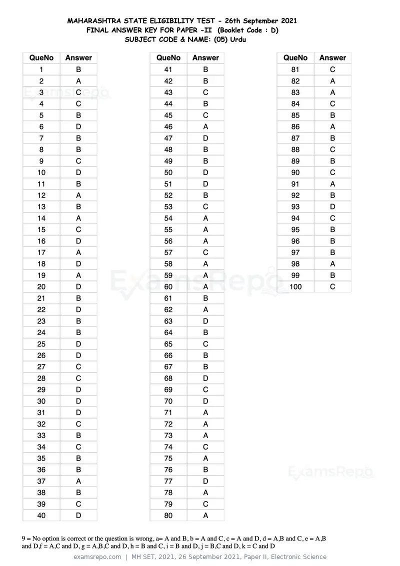
Text of page 20
MAHARASHTRA STATE ELIGIBILITY TEST - 26th September 2021
                    FINAL ANSWER KEY FOR PAPER -II (Booklet Code : D)
                             SUBJECT CODE & NAME: (05) Urdu

  QueNo        Answer                            QueNo        Answer                           QueNo        Answer
      1            B                               41             B                               81              C
      2            A                               42             B                               82              A
      3            C                               43             C                               83              A
      4            C                               44             B                               84              C
      5            B                               45             C                               85              B
      6            D                               46             A                               86              A
      7            B                               47             D                               87              B
      8            B                               48             B                               88              C
      9            C                               49             B                               89              B
     10            D                               50             D                               90              C
     11            B                               51             D                               91              A
     12            A                               52             B                               92              B
     13            B                               53             C                               93              D
     14            A                               54             A                               94              C
     15            C                               55             A                               95              B
     16            D                               56             A                               96              B
     17            A                               57             C                               97              B
     18            D                               58             A                               98              A
     19            A                               59             A                               99              B
     20            D                               60             A                              100              C
     21            B                               61             B
     22            D                               62             A
     23            B                               63             D
     24            B                               64             B
     25            D                               65             C
     26            D                               66             B
     27            C                               67             B
     28            C                               68             D
     29            D                               69             C
     30            D                               70             D
     31            D                               71             A
     32            C                               72             A
     33            B                               73             A
     34            C                               74             C
     35            B                               75             A
     36            B                               76             B
     37            A                               77             D
     38            B                               78             A
     39            C                               79             C
     40            D                               80             A


9 = No option is correct or the question is wrong, a= A and B, b = A and C, c = A and D, d = A,B and C, e = A,B
and D,f = A,C and D, g = A,B,C and D, h = B and C, i = B and D, j = B,C and D, k = C and D
Text of page 21
MAHARASHTRA STATE ELIGIBILITY TEST - 26th September 2021
                    FINAL ANSWER KEY FOR PAPER -II (Booklet Code : A)
                            SUBJECT CODE & NAME: (10) History

  QueNo        Answer                            QueNo        Answer                           QueNo        Answer
      1            D                               41             C                               81              D
      2            D                               42             A                               82              A
      3            D                               43             D                               83              B
      4            D                               44             B                               84              C
      5            A                               45             D                               85              C
      6            B                               46             B                               86              B
      7            C                               47             A                               87              A
      8            D                               48             B                               88              A
      9            B                               49             A                               89              C
     10            C                               50             A                               90              9
     11            B                               51             A                               91              C
     12            A                               52             A                               92              D
     13            C                               53             D                               93              C
     14            B                               54             C                               94              D
     15            A                               55             A                               95              B
     16            A                               56             B                               96              C
     17            A                               57             B                               97              D
     18            B                               58             A                               98              A
     19            A                               59             B                               99              C
     20            C                               60             f                              100              B
     21            A                               61             C
     22            B                               62             A
     23            D                               63             D
     24            A                               64             C
     25            A                               65             C
     26            C                               66             A
     27            B                               67             B
     28            A                               68             C
     29            A                               69             D
     30            C                               70             B
     31            B                               71             C
     32            D                               72             D
     33            C                               73             D
     34            B                               74             B
     35            D                               75             C
     36            A                               76             C
     37            D                               77             C
     38            D                               78             C
     39            A                               79             B
     40            A                               80             C


9 = No option is correct or the question is wrong, a= A and B, b = A and C, c = A and D, d = A,B and C, e = A,B
and D,f = A,C and D, g = A,B,C and D, h = B and C, i = B and D, j = B,C and D, k = C and D
Text of page 22
MAHARASHTRA STATE ELIGIBILITY TEST - 26th September 2021
                    FINAL ANSWER KEY FOR PAPER -II (Booklet Code : B)
                            SUBJECT CODE & NAME: (10) History

  QueNo        Answer                            QueNo        Answer                           QueNo        Answer
      1            A                               41             C                               81              D
      2            B                               42             A                               82              D
      3            D                               43             D                               83              D
      4            A                               44             C                               84              D
      5            A                               45             C                               85              A
      6            C                               46             A                               86              B
      7            B                               47             B                               87              C
      8            A                               48             C                               88              D
      9            A                               49             D                               89              B
     10            C                               50             B                               90              C
     11            B                               51             C                               91              B
     12            D                               52             D                               92              A
     13            C                               53             D                               93              C
     14            B                               54             B                               94              B
     15            D                               55             C                               95              A
     16            A                               56             C                               96              A
     17            D                               57             C                               97              A
     18            D                               58             C                               98              B
     19            A                               59             B                               99              A
     20            A                               60             C                              100              C
     21            C                               61             D
     22            A                               62             A
     23            D                               63             B
     24            B                               64             C
     25            D                               65             C
     26            B                               66             B
     27            A                               67             A
     28            B                               68             A
     29            A                               69             C
     30            A                               70             9
     31            A                               71             C
     32            A                               72             D
     33            D                               73             C
     34            C                               74             D
     35            A                               75             B
     36            B                               76             C
     37            B                               77             D
     38            A                               78             A
     39            B                               79             C
     40             f                              80             B


9 = No option is correct or the question is wrong, a= A and B, b = A and C, c = A and D, d = A,B and C, e = A,B
and D,f = A,C and D, g = A,B,C and D, h = B and C, i = B and D, j = B,C and D, k = C and D
Text of page 23
MAHARASHTRA STATE ELIGIBILITY TEST - 26th September 2021
                    FINAL ANSWER KEY FOR PAPER -II (Booklet Code : C)
                            SUBJECT CODE & NAME: (10) History

  QueNo        Answer                            QueNo        Answer                           QueNo        Answer
      1            C                               41             D                               81              A
      2            A                               42             A                               82              B
      3            D                               43             B                               83              D
      4            B                               44             C                               84              A
      5            D                               45             C                               85              A
      6            B                               46             B                               86              C
      7            A                               47             A                               87              B
      8            B                               48             A                               88              A
      9            A                               49             C                               89              A
     10            A                               50             9                               90              C
     11            A                               51             C                               91              B
     12            A                               52             D                               92              D
     13            D                               53             C                               93              C
     14            C                               54             D                               94              B
     15            A                               55             B                               95              D
     16            B                               56             C                               96              A
     17            B                               57             D                               97              D
     18            A                               58             A                               98              D
     19            B                               59             C                               99              A
     20             f                              60             B                              100              A
     21            C                               61             D
     22            A                               62             D
     23            D                               63             D
     24            C                               64             D
     25            C                               65             A
     26            A                               66             B
     27            B                               67             C
     28            C                               68             D
     29            D                               69             B
     30            B                               70             C
     31            C                               71             B
     32            D                               72             A
     33            D                               73             C
     34            B                               74             B
     35            C                               75             A
     36            C                               76             A
     37            C                               77             A
     38            C                               78             B
     39            B                               79             A
     40            C                               80             C


9 = No option is correct or the question is wrong, a= A and B, b = A and C, c = A and D, d = A,B and C, e = A,B
and D,f = A,C and D, g = A,B,C and D, h = B and C, i = B and D, j = B,C and D, k = C and D
Text of page 24
MAHARASHTRA STATE ELIGIBILITY TEST - 26th September 2021
                    FINAL ANSWER KEY FOR PAPER -II (Booklet Code : D)
                            SUBJECT CODE & NAME: (10) History

  QueNo        Answer                            QueNo        Answer                           QueNo        Answer
      1            C                               41             D                               81              C
      2            A                               42             D                               82              A
      3            D                               43             D                               83              D
      4            C                               44             D                               84              B
      5            C                               45             A                               85              D
      6            A                               46             B                               86              B
      7            B                               47             C                               87              A
      8            C                               48             D                               88              B
      9            D                               49             B                               89              A
     10            B                               50             C                               90              A
     11            C                               51             B                               91              A
     12            D                               52             A                               92              A
     13            D                               53             C                               93              D
     14            B                               54             B                               94              C
     15            C                               55             A                               95              A
     16            C                               56             A                               96              B
     17            C                               57             A                               97              B
     18            C                               58             B                               98              A
     19            B                               59             A                               99              B
     20            C                               60             C                              100              f
     21            D                               61             A
     22            A                               62             B
     23            B                               63             D
     24            C                               64             A
     25            C                               65             A
     26            B                               66             C
     27            A                               67             B
     28            A                               68             A
     29            C                               69             A
     30            9                               70             C
     31            C                               71             B
     32            D                               72             D
     33            C                               73             C
     34            D                               74             B
     35            B                               75             D
     36            C                               76             A
     37            D                               77             D
     38            A                               78             D
     39            C                               79             A
     40            B                               80             A


9 = No option is correct or the question is wrong, a= A and B, b = A and C, c = A and D, d = A,B and C, e = A,B
and D,f = A,C and D, g = A,B,C and D, h = B and C, i = B and D, j = B,C and D, k = C and D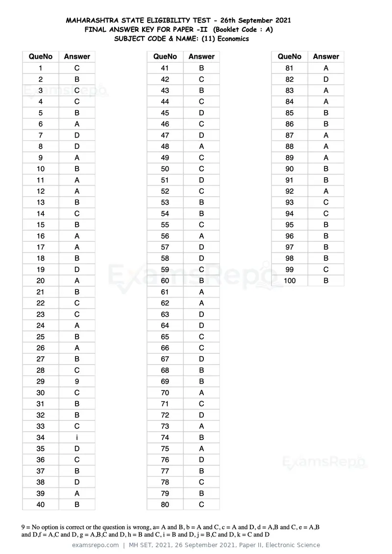
Text of page 25
MAHARASHTRA STATE ELIGIBILITY TEST - 26th September 2021
                    FINAL ANSWER KEY FOR PAPER -II (Booklet Code : A)
                           SUBJECT CODE & NAME: (11) Economics

  QueNo        Answer                            QueNo        Answer                           QueNo        Answer
      1            C                               41             B                               81              A
      2            B                               42             C                               82              D
      3            C                               43             B                               83              A
      4            C                               44             C                               84              A
      5            B                               45             D                               85              B
      6            A                               46             C                               86              B
      7            D                               47             D                               87              A
      8            D                               48             A                               88              A
      9            A                               49             C                               89              A
     10            B                               50             C                               90              B
     11            A                               51             D                               91              B
     12            A                               52             C                               92              A
     13            B                               53             B                               93              C
     14            C                               54             B                               94              C
     15            B                               55             C                               95              B
     16            A                               56             A                               96              B
     17            A                               57             D                               97              B
     18            B                               58             D                               98              B
     19            D                               59             C                               99              C
     20            A                               60             B                              100              B
     21            B                               61             A
     22            C                               62             A
     23            C                               63             D
     24            A                               64             D
     25            B                               65             C
     26            A                               66             C
     27            B                               67             D
     28            C                               68             B
     29            9                               69             B
     30            C                               70             A
     31            B                               71             C
     32            B                               72             D
     33            C                               73             A
     34             i                              74             B
     35            D                               75             A
     36            C                               76             D
     37            B                               77             B
     38            D                               78             C
     39            A                               79             B
     40            B                               80             C


9 = No option is correct or the question is wrong, a= A and B, b = A and C, c = A and D, d = A,B and C, e = A,B
and D,f = A,C and D, g = A,B,C and D, h = B and C, i = B and D, j = B,C and D, k = C and D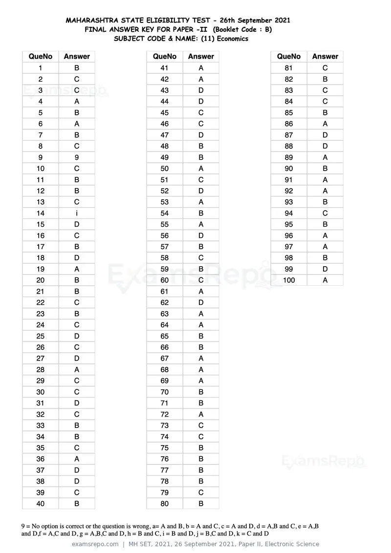
Text of page 26
MAHARASHTRA STATE ELIGIBILITY TEST - 26th September 2021
                    FINAL ANSWER KEY FOR PAPER -II (Booklet Code : B)
                           SUBJECT CODE & NAME: (11) Economics

  QueNo        Answer                            QueNo        Answer                           QueNo        Answer
      1            B                               41             A                               81              C
      2            C                               42             A                               82              B
      3            C                               43             D                               83              C
      4            A                               44             D                               84              C
      5            B                               45             C                               85              B
      6            A                               46             C                               86              A
      7            B                               47             D                               87              D
      8            C                               48             B                               88              D
      9            9                               49             B                               89              A
     10            C                               50             A                               90              B
     11            B                               51             C                               91              A
     12            B                               52             D                               92              A
     13            C                               53             A                               93              B
     14             i                              54             B                               94              C
     15            D                               55             A                               95              B
     16            C                               56             D                               96              A
     17            B                               57             B                               97              A
     18            D                               58             C                               98              B
     19            A                               59             B                               99              D
     20            B                               60             C                              100              A
     21            B                               61             A
     22            C                               62             D
     23            B                               63             A
     24            C                               64             A
     25            D                               65             B
     26            C                               66             B
     27            D                               67             A
     28            A                               68             A
     29            C                               69             A
     30            C                               70             B
     31            D                               71             B
     32            C                               72             A
     33            B                               73             C
     34            B                               74             C
     35            C                               75             B
     36            A                               76             B
     37            D                               77             B
     38            D                               78             B
     39            C                               79             C
     40            B                               80             B


9 = No option is correct or the question is wrong, a= A and B, b = A and C, c = A and D, d = A,B and C, e = A,B
and D,f = A,C and D, g = A,B,C and D, h = B and C, i = B and D, j = B,C and D, k = C and D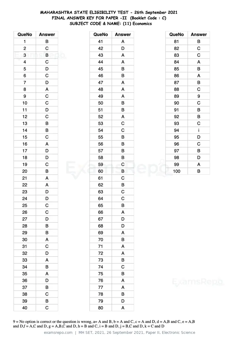
Text of page 27
MAHARASHTRA STATE ELIGIBILITY TEST - 26th September 2021
                    FINAL ANSWER KEY FOR PAPER -II (Booklet Code : C)
                           SUBJECT CODE & NAME: (11) Economics

  QueNo        Answer                            QueNo        Answer                           QueNo        Answer
      1            B                               41             A                               81              B
      2            C                               42             D                               82              C
      3            B                               43             A                               83              C
      4            C                               44             A                               84              A
      5            D                               45             B                               85              B
      6            C                               46             B                               86              A
      7            D                               47             A                               87              B
      8            A                               48             A                               88              C
      9            C                               49             A                               89              9
     10            C                               50             B                               90              C
     11            D                               51             B                               91              B
     12            C                               52             A                               92              B
     13            B                               53             C                               93              C
     14            B                               54             C                               94              i
     15            C                               55             B                               95              D
     16            A                               56             B                               96              C
     17            D                               57             B                               97              B
     18            D                               58             B                               98              D
     19            C                               59             C                               99              A
     20            B                               60             B                              100              B
     21            A                               61             C
     22            A                               62             B
     23            D                               63             C
     24            D                               64             C
     25            C                               65             B
     26            C                               66             A
     27            D                               67             D
     28            B                               68             D
     29            B                               69             A
     30            A                               70             B
     31            C                               71             A
     32            D                               72             A
     33            A                               73             B
     34            B                               74             C
     35            A                               75             B
     36            D                               76             A
     37            B                               77             A
     38            C                               78             B
     39            B                               79             D
     40            C                               80             A


9 = No option is correct or the question is wrong, a= A and B, b = A and C, c = A and D, d = A,B and C, e = A,B
and D,f = A,C and D, g = A,B,C and D, h = B and C, i = B and D, j = B,C and D, k = C and D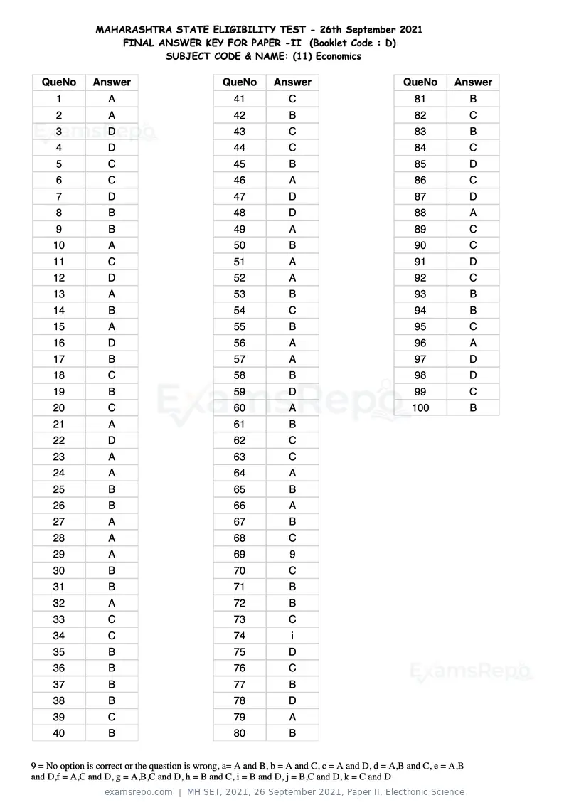
Text of page 28
MAHARASHTRA STATE ELIGIBILITY TEST - 26th September 2021
                    FINAL ANSWER KEY FOR PAPER -II (Booklet Code : D)
                           SUBJECT CODE & NAME: (11) Economics

  QueNo        Answer                            QueNo        Answer                           QueNo        Answer
      1            A                               41             C                               81              B
      2            A                               42             B                               82              C
      3            D                               43             C                               83              B
      4            D                               44             C                               84              C
      5            C                               45             B                               85              D
      6            C                               46             A                               86              C
      7            D                               47             D                               87              D
      8            B                               48             D                               88              A
      9            B                               49             A                               89              C
     10            A                               50             B                               90              C
     11            C                               51             A                               91              D
     12            D                               52             A                               92              C
     13            A                               53             B                               93              B
     14            B                               54             C                               94              B
     15            A                               55             B                               95              C
     16            D                               56             A                               96              A
     17            B                               57             A                               97              D
     18            C                               58             B                               98              D
     19            B                               59             D                               99              C
     20            C                               60             A                              100              B
     21            A                               61             B
     22            D                               62             C
     23            A                               63             C
     24            A                               64             A
     25            B                               65             B
     26            B                               66             A
     27            A                               67             B
     28            A                               68             C
     29            A                               69             9
     30            B                               70             C
     31            B                               71             B
     32            A                               72             B
     33            C                               73             C
     34            C                               74             i
     35            B                               75             D
     36            B                               76             C
     37            B                               77             B
     38            B                               78             D
     39            C                               79             A
     40            B                               80             B


9 = No option is correct or the question is wrong, a= A and B, b = A and C, c = A and D, d = A,B and C, e = A,B
and D,f = A,C and D, g = A,B,C and D, h = B and C, i = B and D, j = B,C and D, k = C and D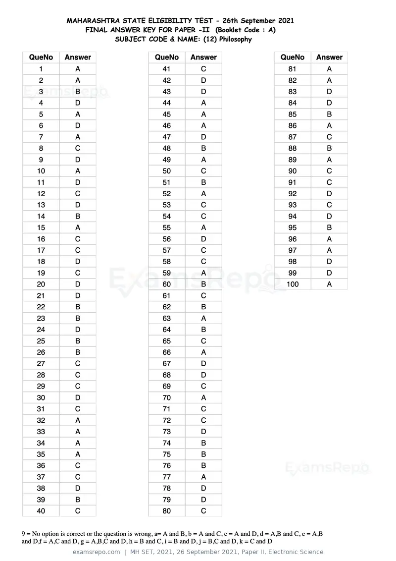
Text of page 29
MAHARASHTRA STATE ELIGIBILITY TEST - 26th September 2021
                    FINAL ANSWER KEY FOR PAPER -II (Booklet Code : A)
                           SUBJECT CODE & NAME: (12) Philosophy

  QueNo        Answer                            QueNo        Answer                           QueNo        Answer
      1            A                               41             C                               81              A
      2            A                               42             D                               82              A
      3            B                               43             D                               83              D
      4            D                               44             A                               84              D
      5            A                               45             A                               85              B
      6            D                               46             A                               86              A
      7            A                               47             D                               87              C
      8            C                               48             B                               88              B
      9            D                               49             A                               89              A
     10            A                               50             C                               90              C
     11            D                               51             B                               91              C
     12            C                               52             A                               92              D
     13            D                               53             C                               93              C
     14            B                               54             C                               94              D
     15            A                               55             A                               95              B
     16            C                               56             D                               96              A
     17            C                               57             C                               97              A
     18            D                               58             C                               98              D
     19            C                               59             A                               99              D
     20            D                               60             B                              100              A
     21            D                               61             C
     22            B                               62             B
     23            B                               63             A
     24            D                               64             B
     25            B                               65             C
     26            B                               66             A
     27            C                               67             D
     28            C                               68             D
     29            C                               69             C
     30            D                               70             A
     31            C                               71             C
     32            A                               72             C
     33            A                               73             D
     34            A                               74             B
     35            A                               75             B
     36            C                               76             B
     37            C                               77             A
     38            D                               78             D
     39            B                               79             D
     40            C                               80             C


9 = No option is correct or the question is wrong, a= A and B, b = A and C, c = A and D, d = A,B and C, e = A,B
and D,f = A,C and D, g = A,B,C and D, h = B and C, i = B and D, j = B,C and D, k = C and D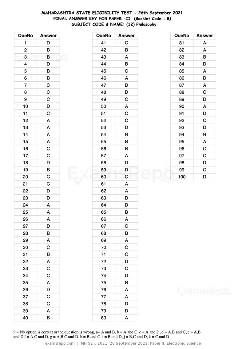
Text of page 30
MAHARASHTRA STATE ELIGIBILITY TEST - 26th September 2021
                    FINAL ANSWER KEY FOR PAPER -II (Booklet Code : B)
                           SUBJECT CODE & NAME: (12) Philosophy

  QueNo        Answer                            QueNo        Answer                           QueNo        Answer
      1            D                               41             C                               81              A
      2            B                               42             B                               82              A
      3            B                               43             A                               83              B
      4            D                               44             B                               84              D
      5            B                               45             C                               85              A
      6            B                               46             A                               86              D
      7            C                               47             D                               87              A
      8            C                               48             D                               88              C
      9            C                               49             C                               89              D
     10            D                               50             A                               90              A
     11            C                               51             C                               91              D
     12            A                               52             C                               92              C
     13            A                               53             D                               93              D
     14            A                               54             B                               94              B
     15            A                               55             B                               95              A
     16            C                               56             B                               96              C
     17            C                               57             A                               97              C
     18            D                               58             D                               98              D
     19            B                               59             D                               99              C
     20            C                               60             C                              100              D
     21            C                               61             A
     22            D                               62             A
     23            D                               63             D
     24            A                               64             D
     25            A                               65             B
     26            A                               66             A
     27            D                               67             C
     28            B                               68             B
     29            A                               69             A
     30            C                               70             C
     31            B                               71             C
     32            A                               72             D
     33            C                               73             C
     34            C                               74             D
     35            A                               75             B
     36            D                               76             A
     37            C                               77             A
     38            C                               78             D
     39            A                               79             D
     40            B                               80             A


9 = No option is correct or the question is wrong, a= A and B, b = A and C, c = A and D, d = A,B and C, e = A,B
and D,f = A,C and D, g = A,B,C and D, h = B and C, i = B and D, j = B,C and D, k = C and D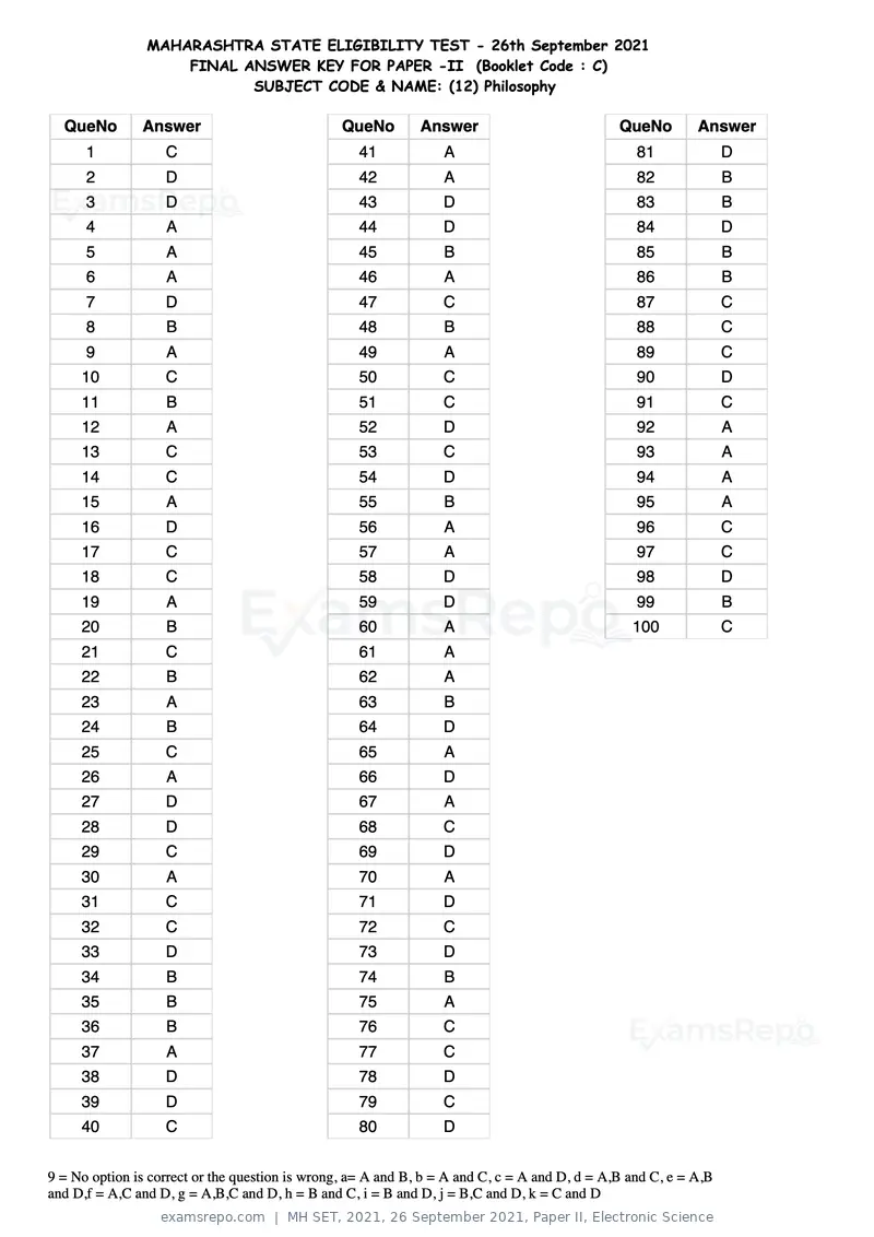
Text of page 31
MAHARASHTRA STATE ELIGIBILITY TEST - 26th September 2021
                    FINAL ANSWER KEY FOR PAPER -II (Booklet Code : C)
                           SUBJECT CODE & NAME: (12) Philosophy

  QueNo        Answer                            QueNo        Answer                           QueNo        Answer
      1            C                               41             A                               81              D
      2            D                               42             A                               82              B
      3            D                               43             D                               83              B
      4            A                               44             D                               84              D
      5            A                               45             B                               85              B
      6            A                               46             A                               86              B
      7            D                               47             C                               87              C
      8            B                               48             B                               88              C
      9            A                               49             A                               89              C
     10            C                               50             C                               90              D
     11            B                               51             C                               91              C
     12            A                               52             D                               92              A
     13            C                               53             C                               93              A
     14            C                               54             D                               94              A
     15            A                               55             B                               95              A
     16            D                               56             A                               96              C
     17            C                               57             A                               97              C
     18            C                               58             D                               98              D
     19            A                               59             D                               99              B
     20            B                               60             A                              100              C
     21            C                               61             A
     22            B                               62             A
     23            A                               63             B
     24            B                               64             D
     25            C                               65             A
     26            A                               66             D
     27            D                               67             A
     28            D                               68             C
     29            C                               69             D
     30            A                               70             A
     31            C                               71             D
     32            C                               72             C
     33            D                               73             D
     34            B                               74             B
     35            B                               75             A
     36            B                               76             C
     37            A                               77             C
     38            D                               78             D
     39            D                               79             C
     40            C                               80             D


9 = No option is correct or the question is wrong, a= A and B, b = A and C, c = A and D, d = A,B and C, e = A,B
and D,f = A,C and D, g = A,B,C and D, h = B and C, i = B and D, j = B,C and D, k = C and D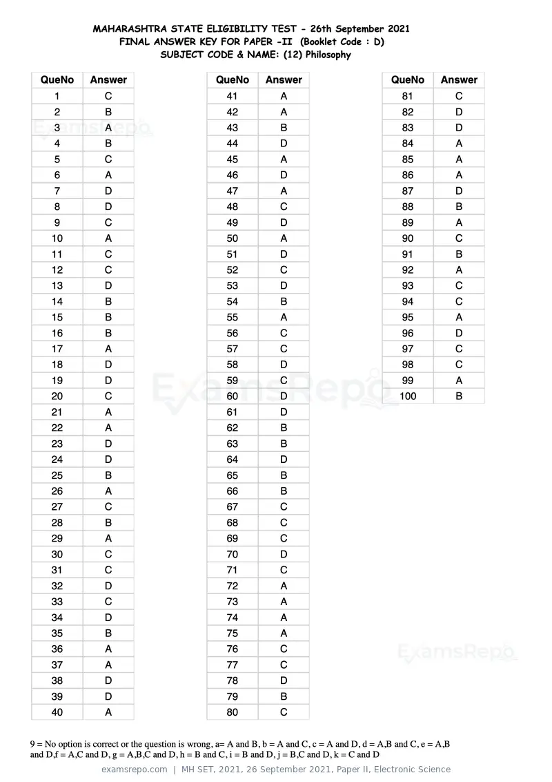
Text of page 32
MAHARASHTRA STATE ELIGIBILITY TEST - 26th September 2021
                    FINAL ANSWER KEY FOR PAPER -II (Booklet Code : D)
                           SUBJECT CODE & NAME: (12) Philosophy

  QueNo        Answer                            QueNo        Answer                           QueNo        Answer
      1            C                               41             A                               81              C
      2            B                               42             A                               82              D
      3            A                               43             B                               83              D
      4            B                               44             D                               84              A
      5            C                               45             A                               85              A
      6            A                               46             D                               86              A
      7            D                               47             A                               87              D
      8            D                               48             C                               88              B
      9            C                               49             D                               89              A
     10            A                               50             A                               90              C
     11            C                               51             D                               91              B
     12            C                               52             C                               92              A
     13            D                               53             D                               93              C
     14            B                               54             B                               94              C
     15            B                               55             A                               95              A
     16            B                               56             C                               96              D
     17            A                               57             C                               97              C
     18            D                               58             D                               98              C
     19            D                               59             C                               99              A
     20            C                               60             D                              100              B
     21            A                               61             D
     22            A                               62             B
     23            D                               63             B
     24            D                               64             D
     25            B                               65             B
     26            A                               66             B
     27            C                               67             C
     28            B                               68             C
     29            A                               69             C
     30            C                               70             D
     31            C                               71             C
     32            D                               72             A
     33            C                               73             A
     34            D                               74             A
     35            B                               75             A
     36            A                               76             C
     37            A                               77             C
     38            D                               78             D
     39            D                               79             B
     40            A                               80             C


9 = No option is correct or the question is wrong, a= A and B, b = A and C, c = A and D, d = A,B and C, e = A,B
and D,f = A,C and D, g = A,B,C and D, h = B and C, i = B and D, j = B,C and D, k = C and D
Text of page 33
MAHARASHTRA STATE ELIGIBILITY TEST - 26th September 2021
                    FINAL ANSWER KEY FOR PAPER -II (Booklet Code : A)
                           SUBJECT CODE & NAME: (13) Psychology

  QueNo        Answer                            QueNo        Answer                           QueNo        Answer
      1            B                               41             C                               81              A
      2            C                               42             B                               82              A
      3            C                               43             A                               83              B
      4            C                               44             A                               84              D
      5            B                               45             A                               85              C
      6            C                               46             C                               86              C
      7            D                               47             A                               87              D
      8            B                               48             B                               88              B
      9            C                               49             B                               89              A
     10            B                               50             A                               90              B
     11            A                               51             D                               91              D
     12            B                               52             C                               92              B
     13            A                               53             B                               93              A
     14            A                               54             C                               94              A
     15            A                               55             A                               95              C
     16            D                               56             A                               96              B
     17            A                               57             B                               97              A
     18            B                               58             C                               98              B
     19            C                               59             A                               99              A
     20            A                               60             B                              100              C
     21            C                               61             B
     22            D                               62             A
     23            D                               63             B
     24            A                               64             B
     25            B                               65             D
     26            A                               66             A
     27            B                               67             B
     28            A                               68             B
     29            A                               69             C
     30            B                               70             C
     31            D                               71             C
     32            A                               72             C
     33            B                               73             B
     34            D                               74             D
     35            A                               75             A
     36            C                               76             C
     37            D                               77             B
     38            B                               78             B
     39            B                               79             C
     40            A                               80             A


9 = No option is correct or the question is wrong, a= A and B, b = A and C, c = A and D, d = A,B and C, e = A,B
and D,f = A,C and D, g = A,B,C and D, h = B and C, i = B and D, j = B,C and D, k = C and D
Text of page 34
MAHARASHTRA STATE ELIGIBILITY TEST - 26th September 2021
                    FINAL ANSWER KEY FOR PAPER -II (Booklet Code : B)
                           SUBJECT CODE & NAME: (13) Psychology

  QueNo        Answer                            QueNo        Answer                           QueNo        Answer
      1            C                               41             B                               81              B
      2            D                               42             A                               82              C
      3            D                               43             B                               83              C
      4            A                               44             B                               84              C
      5            B                               45             D                               85              B
      6            A                               46             A                               86              C
      7            B                               47             B                               87              D
      8            A                               48             B                               88              B
      9            A                               49             C                               89              C
     10            B                               50             C                               90              B
     11            D                               51             C                               91              A
     12            A                               52             C                               92              B
     13            B                               53             B                               93              A
     14            D                               54             D                               94              A
     15            A                               55             A                               95              A
     16            C                               56             C                               96              D
     17            D                               57             B                               97              A
     18            B                               58             B                               98              B
     19            B                               59             C                               99              C
     20            A                               60             A                              100              A
     21            C                               61             A
     22            B                               62             A
     23            A                               63             B
     24            A                               64             D
     25            A                               65             C
     26            C                               66             C
     27            A                               67             D
     28            B                               68             B
     29            B                               69             A
     30            A                               70             B
     31            D                               71             D
     32            C                               72             B
     33            B                               73             A
     34            C                               74             A
     35            A                               75             C
     36            A                               76             B
     37            B                               77             A
     38            C                               78             B
     39            A                               79             A
     40            B                               80             C


9 = No option is correct or the question is wrong, a= A and B, b = A and C, c = A and D, d = A,B and C, e = A,B
and D,f = A,C and D, g = A,B,C and D, h = B and C, i = B and D, j = B,C and D, k = C and D
Text of page 35
MAHARASHTRA STATE ELIGIBILITY TEST - 26th September 2021
                    FINAL ANSWER KEY FOR PAPER -II (Booklet Code : C)
                           SUBJECT CODE & NAME: (13) Psychology

  QueNo        Answer                            QueNo        Answer                           QueNo        Answer
      1            C                               41             A                               81              C
      2            B                               42             A                               82              D
      3            A                               43             B                               83              D
      4            A                               44             D                               84              A
      5            A                               45             C                               85              B
      6            C                               46             C                               86              A
      7            A                               47             D                               87              B
      8            B                               48             B                               88              A
      9            B                               49             A                               89              A
     10            A                               50             B                               90              B
     11            D                               51             D                               91              D
     12            C                               52             B                               92              A
     13            B                               53             A                               93              B
     14            C                               54             A                               94              D
     15            A                               55             C                               95              A
     16            A                               56             B                               96              C
     17            B                               57             A                               97              D
     18            C                               58             B                               98              B
     19            A                               59             A                               99              B
     20            B                               60             C                              100              A
     21            B                               61             B
     22            A                               62             C
     23            B                               63             C
     24            B                               64             C
     25            D                               65             B
     26            A                               66             C
     27            B                               67             D
     28            B                               68             B
     29            C                               69             C
     30            C                               70             B
     31            C                               71             A
     32            C                               72             B
     33            B                               73             A
     34            D                               74             A
     35            A                               75             A
     36            C                               76             D
     37            B                               77             A
     38            B                               78             B
     39            C                               79             C
     40            A                               80             A


9 = No option is correct or the question is wrong, a= A and B, b = A and C, c = A and D, d = A,B and C, e = A,B
and D,f = A,C and D, g = A,B,C and D, h = B and C, i = B and D, j = B,C and D, k = C and D
Text of page 36
MAHARASHTRA STATE ELIGIBILITY TEST - 26th September 2021
                    FINAL ANSWER KEY FOR PAPER -II (Booklet Code : D)
                           SUBJECT CODE & NAME: (13) Psychology

  QueNo        Answer                            QueNo        Answer                           QueNo        Answer
      1            B                               41             B                               81              C
      2            A                               42             C                               82              B
      3            B                               43             C                               83              A
      4            B                               44             C                               84              A
      5            D                               45             B                               85              A
      6            A                               46             C                               86              C
      7            B                               47             D                               87              A
      8            B                               48             B                               88              B
      9            C                               49             C                               89              B
     10            C                               50             B                               90              A
     11            C                               51             A                               91              D
     12            C                               52             B                               92              C
     13            B                               53             A                               93              B
     14            D                               54             A                               94              C
     15            A                               55             A                               95              A
     16            C                               56             D                               96              A
     17            B                               57             A                               97              B
     18            B                               58             B                               98              C
     19            C                               59             C                               99              A
     20            A                               60             A                              100              B
     21            A                               61             C
     22            A                               62             D
     23            B                               63             D
     24            D                               64             A
     25            C                               65             B
     26            C                               66             A
     27            D                               67             B
     28            B                               68             A
     29            A                               69             A
     30            B                               70             B
     31            D                               71             D
     32            B                               72             A
     33            A                               73             B
     34            A                               74             D
     35            C                               75             A
     36            B                               76             C
     37            A                               77             D
     38            B                               78             B
     39            A                               79             B
     40            C                               80             A


9 = No option is correct or the question is wrong, a= A and B, b = A and C, c = A and D, d = A,B and C, e = A,B
and D,f = A,C and D, g = A,B,C and D, h = B and C, i = B and D, j = B,C and D, k = C and D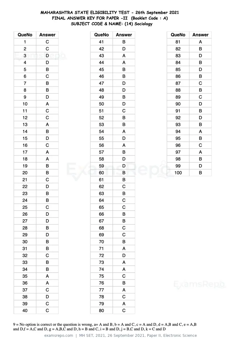
Text of page 37
MAHARASHTRA STATE ELIGIBILITY TEST - 26th September 2021
                    FINAL ANSWER KEY FOR PAPER -II (Booklet Code : A)
                           SUBJECT CODE & NAME: (14) Sociology

  QueNo        Answer                            QueNo        Answer                           QueNo        Answer
      1            C                               41             B                               81              A
      2            C                               42             D                               82              B
      3            D                               43             A                               83              D
      4            D                               44             A                               84              B
      5            B                               45             B                               85              D
      6            C                               46             B                               86              B
      7            B                               47             D                               87              C
      8            B                               48             D                               88              B
      9            D                               49             B                               89              C
     10            A                               50             D                               90              D
     11            C                               51             C                               91              B
     12            C                               52             B                               92              D
     13            A                               53             B                               93              B
     14            B                               54             A                               94              A
     15            D                               55             D                               95              B
     16            C                               56             A                               96              C
     17            A                               57             B                               97              A
     18            A                               58             D                               98              B
     19            B                               59             D                               99              D
     20            B                               60             B                              100              B
     21            C                               61             B
     22            D                               62             C
     23            B                               63             B
     24            B                               64             C
     25            C                               65             C
     26            D                               66             B
     27            D                               67             B
     28            B                               68             C
     29            D                               69             C
     30            B                               70             B
     31            B                               71             A
     32            C                               72             D
     33            B                               73             A
     34            B                               74             A
     35            A                               75             C
     36            A                               76             B
     37            C                               77             A
     38            D                               78             C
     39            C                               79             A
     40            C                               80             C


9 = No option is correct or the question is wrong, a= A and B, b = A and C, c = A and D, d = A,B and C, e = A,B
and D,f = A,C and D, g = A,B,C and D, h = B and C, i = B and D, j = B,C and D, k = C and D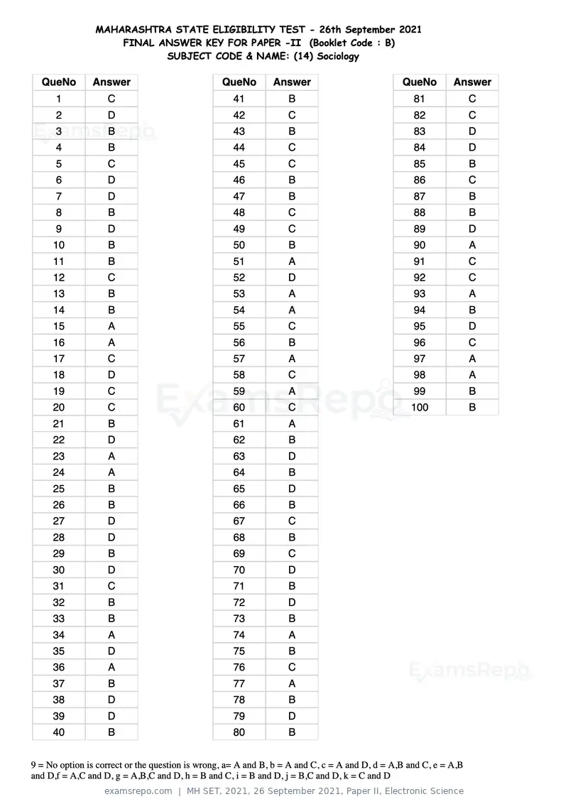
Text of page 38
MAHARASHTRA STATE ELIGIBILITY TEST - 26th September 2021
                    FINAL ANSWER KEY FOR PAPER -II (Booklet Code : B)
                           SUBJECT CODE & NAME: (14) Sociology

  QueNo        Answer                            QueNo        Answer                           QueNo        Answer
      1            C                               41             B                               81              C
      2            D                               42             C                               82              C
      3            B                               43             B                               83              D
      4            B                               44             C                               84              D
      5            C                               45             C                               85              B
      6            D                               46             B                               86              C
      7            D                               47             B                               87              B
      8            B                               48             C                               88              B
      9            D                               49             C                               89              D
     10            B                               50             B                               90              A
     11            B                               51             A                               91              C
     12            C                               52             D                               92              C
     13            B                               53             A                               93              A
     14            B                               54             A                               94              B
     15            A                               55             C                               95              D
     16            A                               56             B                               96              C
     17            C                               57             A                               97              A
     18            D                               58             C                               98              A
     19            C                               59             A                               99              B
     20            C                               60             C                              100              B
     21            B                               61             A
     22            D                               62             B
     23            A                               63             D
     24            A                               64             B
     25            B                               65             D
     26            B                               66             B
     27            D                               67             C
     28            D                               68             B
     29            B                               69             C
     30            D                               70             D
     31            C                               71             B
     32            B                               72             D
     33            B                               73             B
     34            A                               74             A
     35            D                               75             B
     36            A                               76             C
     37            B                               77             A
     38            D                               78             B
     39            D                               79             D
     40            B                               80             B


9 = No option is correct or the question is wrong, a= A and B, b = A and C, c = A and D, d = A,B and C, e = A,B
and D,f = A,C and D, g = A,B,C and D, h = B and C, i = B and D, j = B,C and D, k = C and D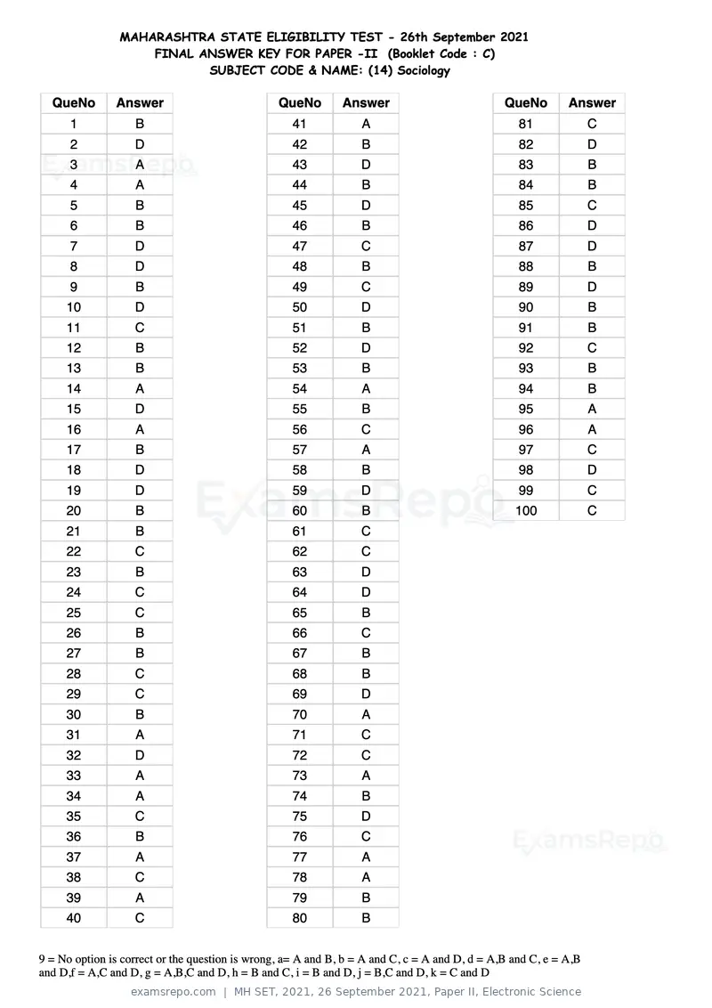
Text of page 39
MAHARASHTRA STATE ELIGIBILITY TEST - 26th September 2021
                    FINAL ANSWER KEY FOR PAPER -II (Booklet Code : C)
                           SUBJECT CODE & NAME: (14) Sociology

  QueNo        Answer                            QueNo        Answer                           QueNo        Answer
      1            B                               41             A                               81              C
      2            D                               42             B                               82              D
      3            A                               43             D                               83              B
      4            A                               44             B                               84              B
      5            B                               45             D                               85              C
      6            B                               46             B                               86              D
      7            D                               47             C                               87              D
      8            D                               48             B                               88              B
      9            B                               49             C                               89              D
     10            D                               50             D                               90              B
     11            C                               51             B                               91              B
     12            B                               52             D                               92              C
     13            B                               53             B                               93              B
     14            A                               54             A                               94              B
     15            D                               55             B                               95              A
     16            A                               56             C                               96              A
     17            B                               57             A                               97              C
     18            D                               58             B                               98              D
     19            D                               59             D                               99              C
     20            B                               60             B                              100              C
     21            B                               61             C
     22            C                               62             C
     23            B                               63             D
     24            C                               64             D
     25            C                               65             B
     26            B                               66             C
     27            B                               67             B
     28            C                               68             B
     29            C                               69             D
     30            B                               70             A
     31            A                               71             C
     32            D                               72             C
     33            A                               73             A
     34            A                               74             B
     35            C                               75             D
     36            B                               76             C
     37            A                               77             A
     38            C                               78             A
     39            A                               79             B
     40            C                               80             B


9 = No option is correct or the question is wrong, a= A and B, b = A and C, c = A and D, d = A,B and C, e = A,B
and D,f = A,C and D, g = A,B,C and D, h = B and C, i = B and D, j = B,C and D, k = C and D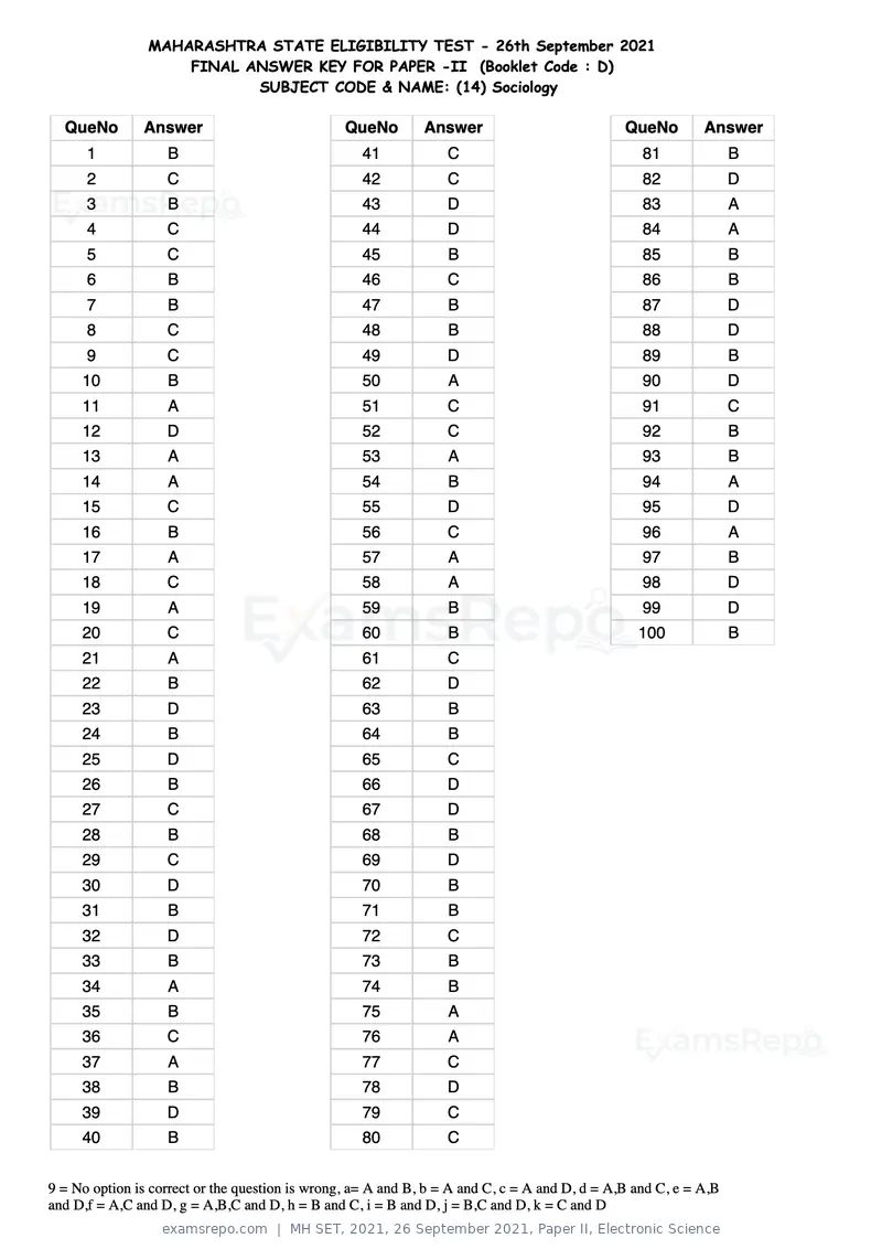
Text of page 40
MAHARASHTRA STATE ELIGIBILITY TEST - 26th September 2021
                    FINAL ANSWER KEY FOR PAPER -II (Booklet Code : D)
                           SUBJECT CODE & NAME: (14) Sociology

  QueNo        Answer                            QueNo        Answer                           QueNo        Answer
      1            B                               41             C                               81              B
      2            C                               42             C                               82              D
      3            B                               43             D                               83              A
      4            C                               44             D                               84              A
      5            C                               45             B                               85              B
      6            B                               46             C                               86              B
      7            B                               47             B                               87              D
      8            C                               48             B                               88              D
      9            C                               49             D                               89              B
     10            B                               50             A                               90              D
     11            A                               51             C                               91              C
     12            D                               52             C                               92              B
     13            A                               53             A                               93              B
     14            A                               54             B                               94              A
     15            C                               55             D                               95              D
     16            B                               56             C                               96              A
     17            A                               57             A                               97              B
     18            C                               58             A                               98              D
     19            A                               59             B                               99              D
     20            C                               60             B                              100              B
     21            A                               61             C
     22            B                               62             D
     23            D                               63             B
     24            B                               64             B
     25            D                               65             C
     26            B                               66             D
     27            C                               67             D
     28            B                               68             B
     29            C                               69             D
     30            D                               70             B
     31            B                               71             B
     32            D                               72             C
     33            B                               73             B
     34            A                               74             B
     35            B                               75             A
     36            C                               76             A
     37            A                               77             C
     38            B                               78             D
     39            D                               79             C
     40            B                               80             C


9 = No option is correct or the question is wrong, a= A and B, b = A and C, c = A and D, d = A,B and C, e = A,B
and D,f = A,C and D, g = A,B,C and D, h = B and C, i = B and D, j = B,C and D, k = C and D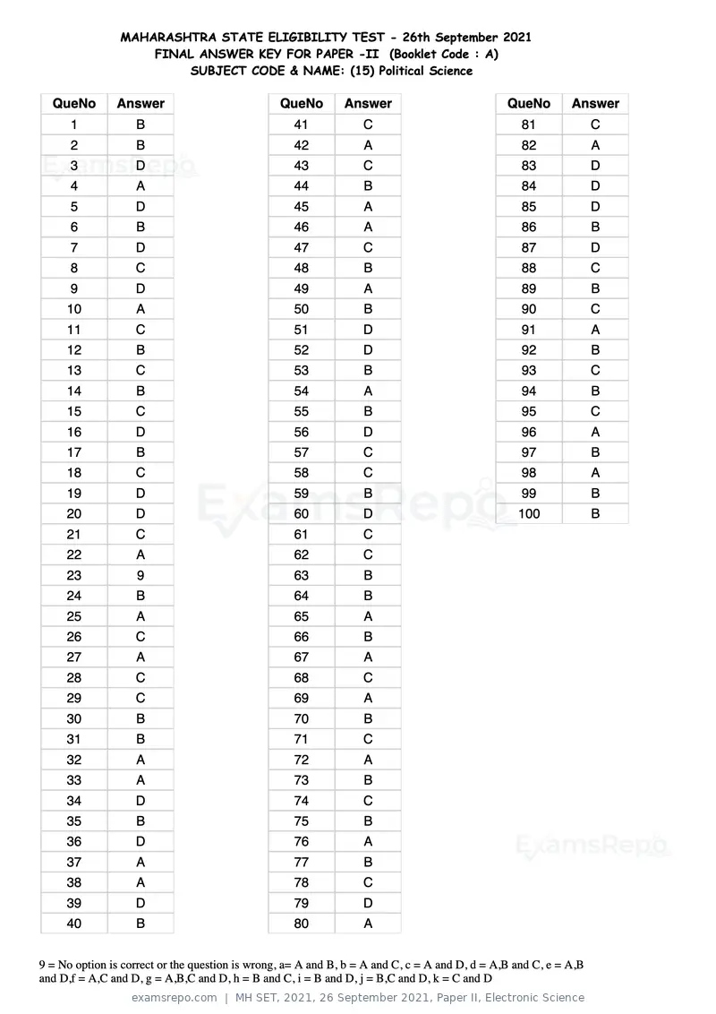
Text of page 41
MAHARASHTRA STATE ELIGIBILITY TEST - 26th September 2021
                    FINAL ANSWER KEY FOR PAPER -II (Booklet Code : A)
                        SUBJECT CODE & NAME: (15) Political Science

  QueNo        Answer                            QueNo        Answer                           QueNo        Answer
      1            B                               41             C                               81              C
      2            B                               42             A                               82              A
      3            D                               43             C                               83              D
      4            A                               44             B                               84              D
      5            D                               45             A                               85              D
      6            B                               46             A                               86              B
      7            D                               47             C                               87              D
      8            C                               48             B                               88              C
      9            D                               49             A                               89              B
     10            A                               50             B                               90              C
     11            C                               51             D                               91              A
     12            B                               52             D                               92              B
     13            C                               53             B                               93              C
     14            B                               54             A                               94              B
     15            C                               55             B                               95              C
     16            D                               56             D                               96              A
     17            B                               57             C                               97              B
     18            C                               58             C                               98              A
     19            D                               59             B                               99              B
     20            D                               60             D                              100              B
     21            C                               61             C
     22            A                               62             C
     23            9                               63             B
     24            B                               64             B
     25            A                               65             A
     26            C                               66             B
     27            A                               67             A
     28            C                               68             C
     29            C                               69             A
     30            B                               70             B
     31            B                               71             C
     32            A                               72             A
     33            A                               73             B
     34            D                               74             C
     35            B                               75             B
     36            D                               76             A
     37            A                               77             B
     38            A                               78             C
     39            D                               79             D
     40            B                               80             A


9 = No option is correct or the question is wrong, a= A and B, b = A and C, c = A and D, d = A,B and C, e = A,B
and D,f = A,C and D, g = A,B,C and D, h = B and C, i = B and D, j = B,C and D, k = C and D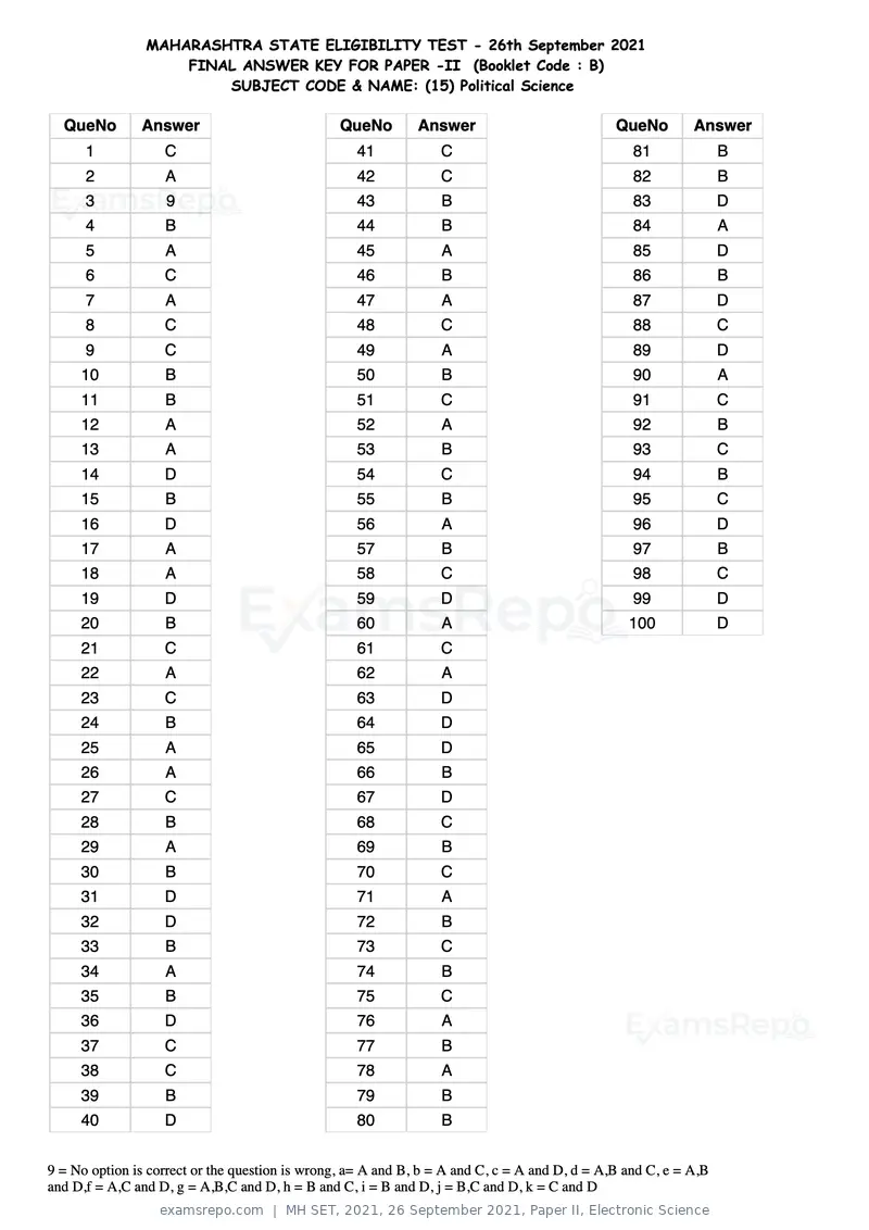
Text of page 42
MAHARASHTRA STATE ELIGIBILITY TEST - 26th September 2021
                    FINAL ANSWER KEY FOR PAPER -II (Booklet Code : B)
                        SUBJECT CODE & NAME: (15) Political Science

  QueNo        Answer                            QueNo        Answer                           QueNo        Answer
      1            C                               41             C                               81              B
      2            A                               42             C                               82              B
      3            9                               43             B                               83              D
      4            B                               44             B                               84              A
      5            A                               45             A                               85              D
      6            C                               46             B                               86              B
      7            A                               47             A                               87              D
      8            C                               48             C                               88              C
      9            C                               49             A                               89              D
     10            B                               50             B                               90              A
     11            B                               51             C                               91              C
     12            A                               52             A                               92              B
     13            A                               53             B                               93              C
     14            D                               54             C                               94              B
     15            B                               55             B                               95              C
     16            D                               56             A                               96              D
     17            A                               57             B                               97              B
     18            A                               58             C                               98              C
     19            D                               59             D                               99              D
     20            B                               60             A                              100              D
     21            C                               61             C
     22            A                               62             A
     23            C                               63             D
     24            B                               64             D
     25            A                               65             D
     26            A                               66             B
     27            C                               67             D
     28            B                               68             C
     29            A                               69             B
     30            B                               70             C
     31            D                               71             A
     32            D                               72             B
     33            B                               73             C
     34            A                               74             B
     35            B                               75             C
     36            D                               76             A
     37            C                               77             B
     38            C                               78             A
     39            B                               79             B
     40            D                               80             B


9 = No option is correct or the question is wrong, a= A and B, b = A and C, c = A and D, d = A,B and C, e = A,B
and D,f = A,C and D, g = A,B,C and D, h = B and C, i = B and D, j = B,C and D, k = C and D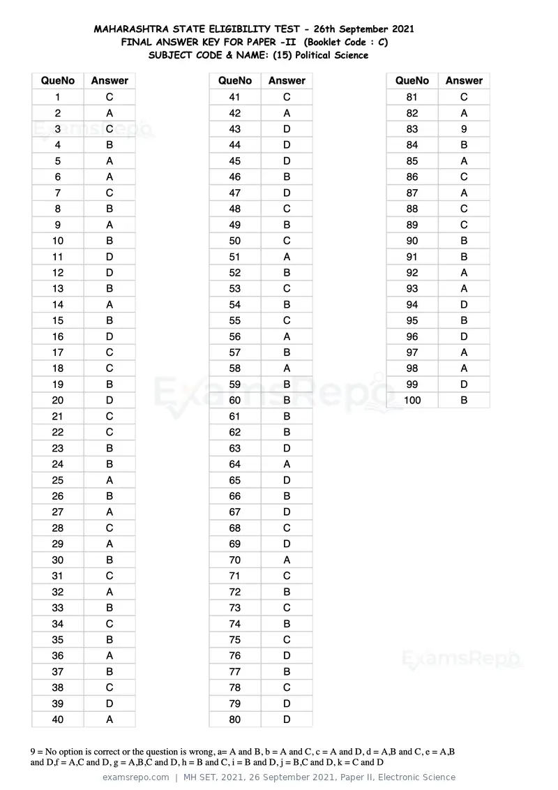
Text of page 43
MAHARASHTRA STATE ELIGIBILITY TEST - 26th September 2021
                    FINAL ANSWER KEY FOR PAPER -II (Booklet Code : C)
                        SUBJECT CODE & NAME: (15) Political Science

  QueNo        Answer                            QueNo        Answer                           QueNo        Answer
      1            C                               41             C                               81              C
      2            A                               42             A                               82              A
      3            C                               43             D                               83              9
      4            B                               44             D                               84              B
      5            A                               45             D                               85              A
      6            A                               46             B                               86              C
      7            C                               47             D                               87              A
      8            B                               48             C                               88              C
      9            A                               49             B                               89              C
     10            B                               50             C                               90              B
     11            D                               51             A                               91              B
     12            D                               52             B                               92              A
     13            B                               53             C                               93              A
     14            A                               54             B                               94              D
     15            B                               55             C                               95              B
     16            D                               56             A                               96              D
     17            C                               57             B                               97              A
     18            C                               58             A                               98              A
     19            B                               59             B                               99              D
     20            D                               60             B                              100              B
     21            C                               61             B
     22            C                               62             B
     23            B                               63             D
     24            B                               64             A
     25            A                               65             D
     26            B                               66             B
     27            A                               67             D
     28            C                               68             C
     29            A                               69             D
     30            B                               70             A
     31            C                               71             C
     32            A                               72             B
     33            B                               73             C
     34            C                               74             B
     35            B                               75             C
     36            A                               76             D
     37            B                               77             B
     38            C                               78             C
     39            D                               79             D
     40            A                               80             D


9 = No option is correct or the question is wrong, a= A and B, b = A and C, c = A and D, d = A,B and C, e = A,B
and D,f = A,C and D, g = A,B,C and D, h = B and C, i = B and D, j = B,C and D, k = C and D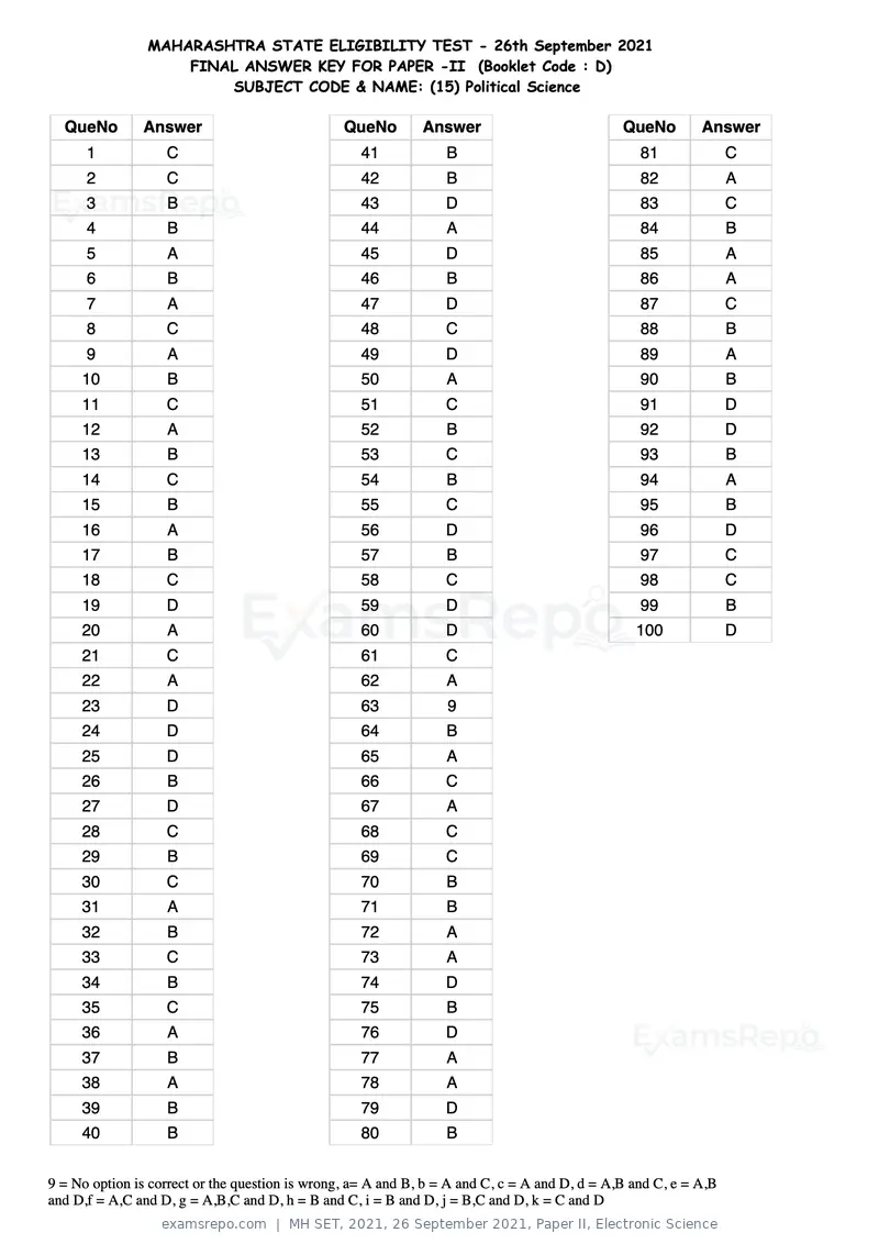
Text of page 44
MAHARASHTRA STATE ELIGIBILITY TEST - 26th September 2021
                    FINAL ANSWER KEY FOR PAPER -II (Booklet Code : D)
                        SUBJECT CODE & NAME: (15) Political Science

  QueNo        Answer                            QueNo        Answer                           QueNo        Answer
      1            C                               41             B                               81              C
      2            C                               42             B                               82              A
      3            B                               43             D                               83              C
      4            B                               44             A                               84              B
      5            A                               45             D                               85              A
      6            B                               46             B                               86              A
      7            A                               47             D                               87              C
      8            C                               48             C                               88              B
      9            A                               49             D                               89              A
     10            B                               50             A                               90              B
     11            C                               51             C                               91              D
     12            A                               52             B                               92              D
     13            B                               53             C                               93              B
     14            C                               54             B                               94              A
     15            B                               55             C                               95              B
     16            A                               56             D                               96              D
     17            B                               57             B                               97              C
     18            C                               58             C                               98              C
     19            D                               59             D                               99              B
     20            A                               60             D                              100              D
     21            C                               61             C
     22            A                               62             A
     23            D                               63             9
     24            D                               64             B
     25            D                               65             A
     26            B                               66             C
     27            D                               67             A
     28            C                               68             C
     29            B                               69             C
     30            C                               70             B
     31            A                               71             B
     32            B                               72             A
     33            C                               73             A
     34            B                               74             D
     35            C                               75             B
     36            A                               76             D
     37            B                               77             A
     38            A                               78             A
     39            B                               79             D
     40            B                               80             B


9 = No option is correct or the question is wrong, a= A and B, b = A and C, c = A and D, d = A,B and C, e = A,B
and D,f = A,C and D, g = A,B,C and D, h = B and C, i = B and D, j = B,C and D, k = C and D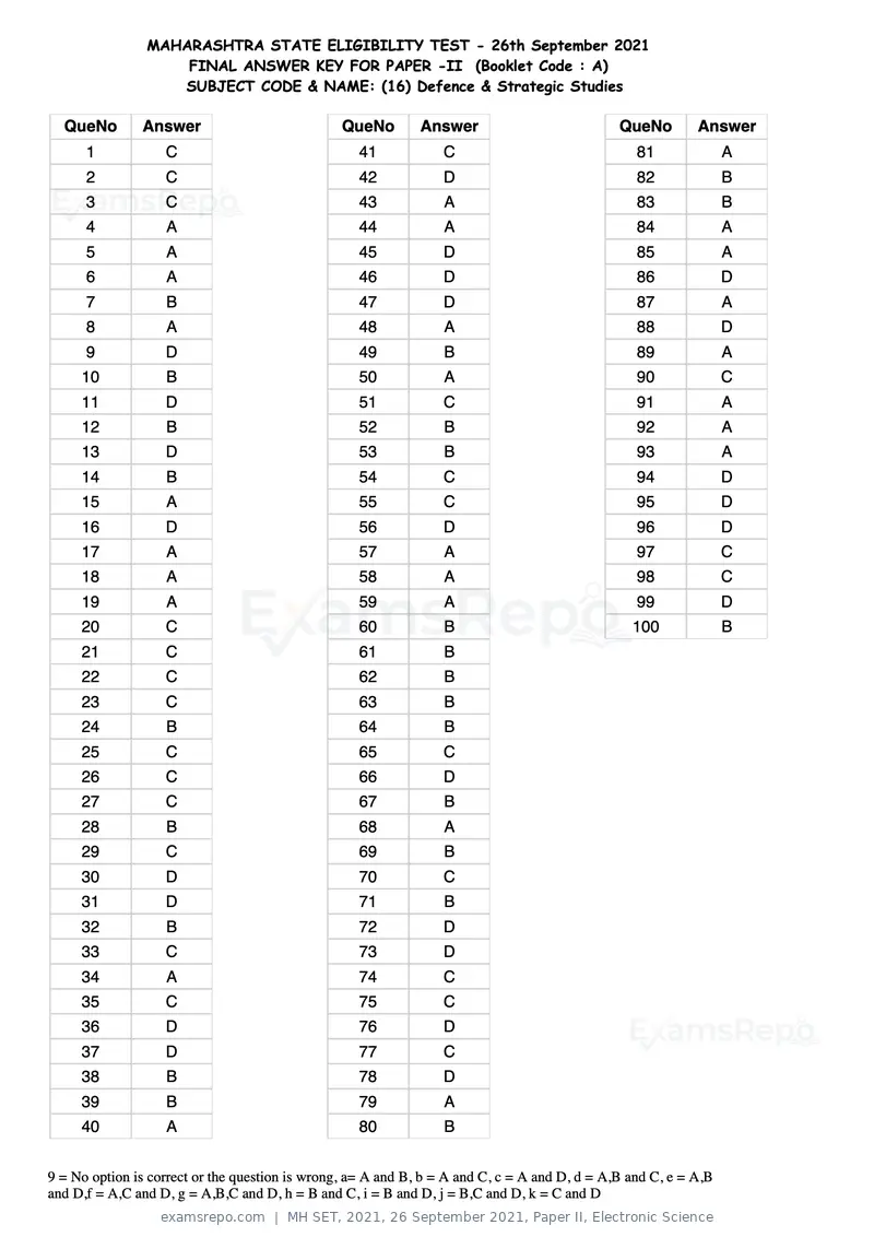
Text of page 45
MAHARASHTRA STATE ELIGIBILITY TEST - 26th September 2021
                    FINAL ANSWER KEY FOR PAPER -II (Booklet Code : A)
                   SUBJECT CODE & NAME: (16) Defence & Strategic Studies

  QueNo        Answer                            QueNo        Answer                           QueNo        Answer
      1            C                               41             C                               81              A
      2            C                               42             D                               82              B
      3            C                               43             A                               83              B
      4            A                               44             A                               84              A
      5            A                               45             D                               85              A
      6            A                               46             D                               86              D
      7            B                               47             D                               87              A
      8            A                               48             A                               88              D
      9            D                               49             B                               89              A
     10            B                               50             A                               90              C
     11            D                               51             C                               91              A
     12            B                               52             B                               92              A
     13            D                               53             B                               93              A
     14            B                               54             C                               94              D
     15            A                               55             C                               95              D
     16            D                               56             D                               96              D
     17            A                               57             A                               97              C
     18            A                               58             A                               98              C
     19            A                               59             A                               99              D
     20            C                               60             B                              100              B
     21            C                               61             B
     22            C                               62             B
     23            C                               63             B
     24            B                               64             B
     25            C                               65             C
     26            C                               66             D
     27            C                               67             B
     28            B                               68             A
     29            C                               69             B
     30            D                               70             C
     31            D                               71             B
     32            B                               72             D
     33            C                               73             D
     34            A                               74             C
     35            C                               75             C
     36            D                               76             D
     37            D                               77             C
     38            B                               78             D
     39            B                               79             A
     40            A                               80             B


9 = No option is correct or the question is wrong, a= A and B, b = A and C, c = A and D, d = A,B and C, e = A,B
and D,f = A,C and D, g = A,B,C and D, h = B and C, i = B and D, j = B,C and D, k = C and D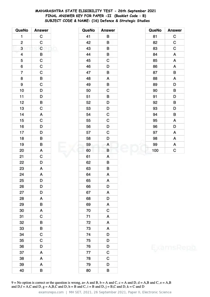
Text of page 46
MAHARASHTRA STATE ELIGIBILITY TEST - 26th September 2021
                    FINAL ANSWER KEY FOR PAPER -II (Booklet Code : B)
                   SUBJECT CODE & NAME: (16) Defence & Strategic Studies

  QueNo        Answer                            QueNo        Answer                           QueNo        Answer
      1            C                               41             B                               81              C
      2            C                               42             B                               82              C
      3            C                               43             B                               83              C
      4            B                               44             B                               84              A
      5            C                               45             C                               85              A
      6            C                               46             D                               86              A
      7            C                               47             B                               87              B
      8            B                               48             A                               88              A
      9            C                               49             B                               89              D
     10            D                               50             C                               90              B
     11            D                               51             B                               91              D
     12            B                               52             D                               92              B
     13            C                               53             D                               93              D
     14            A                               54             C                               94              B
     15            C                               55             C                               95              A
     16            D                               56             D                               96              D
     17            D                               57             C                               97              A
     18            B                               58             D                               98              A
     19            B                               59             A                               99              A
     20            A                               60             B                              100              C
     21            C                               61             A
     22            D                               62             B
     23            A                               63             B
     24            A                               64             A
     25            D                               65             A
     26            D                               66             D
     27            D                               67             A
     28            A                               68             D
     29            B                               69             A
     30            A                               70             C
     31            C                               71             A
     32            B                               72             A
     33            B                               73             A
     34            C                               74             D
     35            C                               75             D
     36            D                               76             D
     37            A                               77             C
     38            A                               78             C
     39            A                               79             D
     40            B                               80             B


9 = No option is correct or the question is wrong, a= A and B, b = A and C, c = A and D, d = A,B and C, e = A,B
and D,f = A,C and D, g = A,B,C and D, h = B and C, i = B and D, j = B,C and D, k = C and D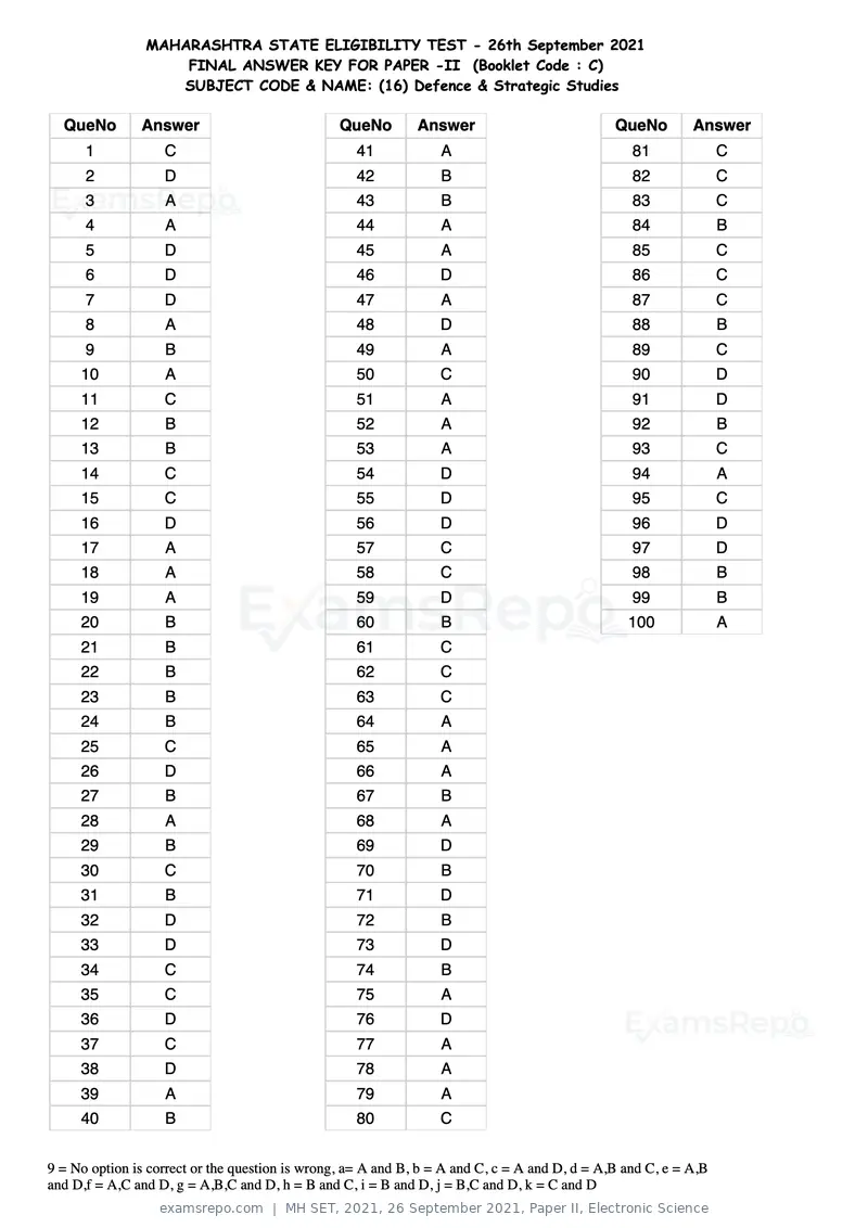
Text of page 47
MAHARASHTRA STATE ELIGIBILITY TEST - 26th September 2021
                    FINAL ANSWER KEY FOR PAPER -II (Booklet Code : C)
                   SUBJECT CODE & NAME: (16) Defence & Strategic Studies

  QueNo        Answer                            QueNo        Answer                           QueNo        Answer
      1            C                               41             A                               81              C
      2            D                               42             B                               82              C
      3            A                               43             B                               83              C
      4            A                               44             A                               84              B
      5            D                               45             A                               85              C
      6            D                               46             D                               86              C
      7            D                               47             A                               87              C
      8            A                               48             D                               88              B
      9            B                               49             A                               89              C
     10            A                               50             C                               90              D
     11            C                               51             A                               91              D
     12            B                               52             A                               92              B
     13            B                               53             A                               93              C
     14            C                               54             D                               94              A
     15            C                               55             D                               95              C
     16            D                               56             D                               96              D
     17            A                               57             C                               97              D
     18            A                               58             C                               98              B
     19            A                               59             D                               99              B
     20            B                               60             B                              100              A
     21            B                               61             C
     22            B                               62             C
     23            B                               63             C
     24            B                               64             A
     25            C                               65             A
     26            D                               66             A
     27            B                               67             B
     28            A                               68             A
     29            B                               69             D
     30            C                               70             B
     31            B                               71             D
     32            D                               72             B
     33            D                               73             D
     34            C                               74             B
     35            C                               75             A
     36            D                               76             D
     37            C                               77             A
     38            D                               78             A
     39            A                               79             A
     40            B                               80             C


9 = No option is correct or the question is wrong, a= A and B, b = A and C, c = A and D, d = A,B and C, e = A,B
and D,f = A,C and D, g = A,B,C and D, h = B and C, i = B and D, j = B,C and D, k = C and D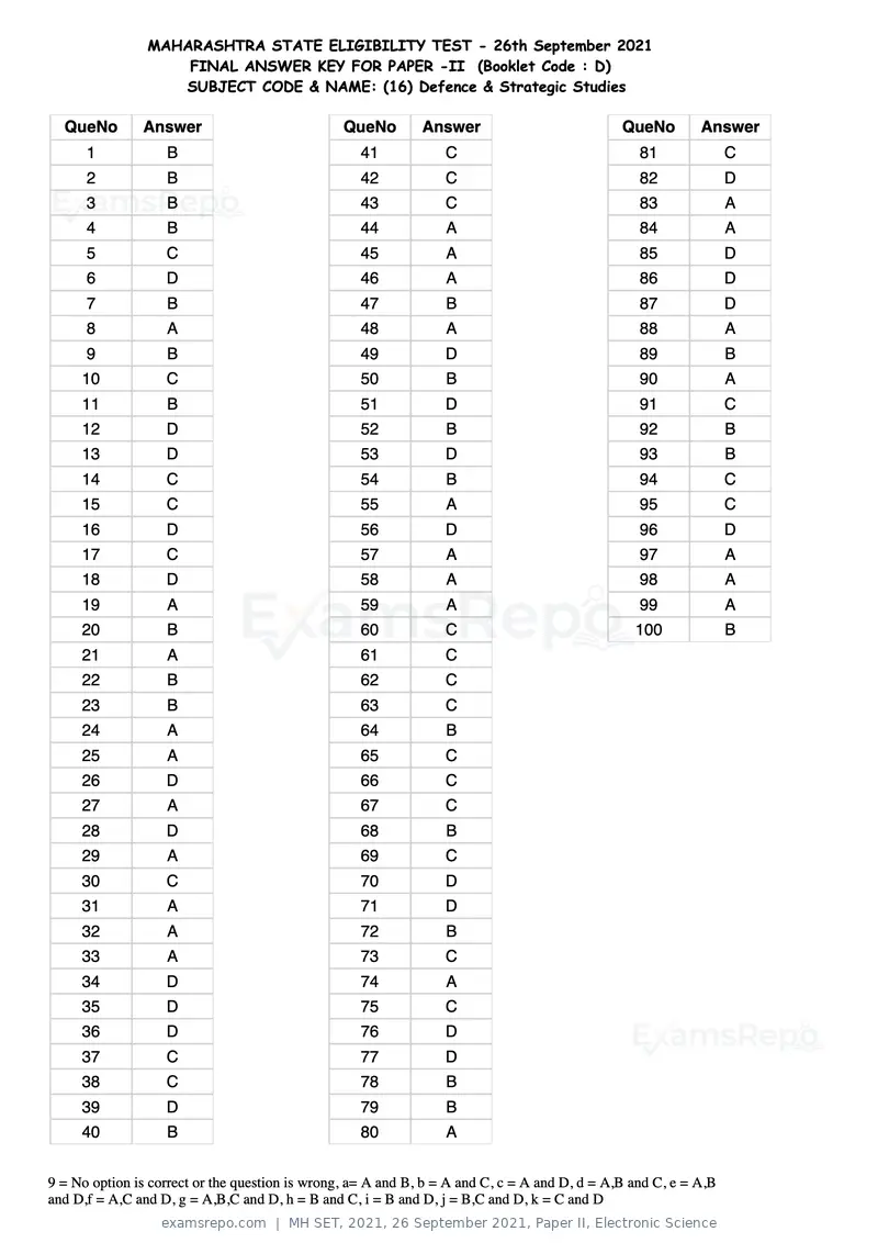
Text of page 48
MAHARASHTRA STATE ELIGIBILITY TEST - 26th September 2021
                    FINAL ANSWER KEY FOR PAPER -II (Booklet Code : D)
                   SUBJECT CODE & NAME: (16) Defence & Strategic Studies

  QueNo        Answer                            QueNo        Answer                           QueNo        Answer
      1            B                               41             C                               81              C
      2            B                               42             C                               82              D
      3            B                               43             C                               83              A
      4            B                               44             A                               84              A
      5            C                               45             A                               85              D
      6            D                               46             A                               86              D
      7            B                               47             B                               87              D
      8            A                               48             A                               88              A
      9            B                               49             D                               89              B
     10            C                               50             B                               90              A
     11            B                               51             D                               91              C
     12            D                               52             B                               92              B
     13            D                               53             D                               93              B
     14            C                               54             B                               94              C
     15            C                               55             A                               95              C
     16            D                               56             D                               96              D
     17            C                               57             A                               97              A
     18            D                               58             A                               98              A
     19            A                               59             A                               99              A
     20            B                               60             C                              100              B
     21            A                               61             C
     22            B                               62             C
     23            B                               63             C
     24            A                               64             B
     25            A                               65             C
     26            D                               66             C
     27            A                               67             C
     28            D                               68             B
     29            A                               69             C
     30            C                               70             D
     31            A                               71             D
     32            A                               72             B
     33            A                               73             C
     34            D                               74             A
     35            D                               75             C
     36            D                               76             D
     37            C                               77             D
     38            C                               78             B
     39            D                               79             B
     40            B                               80             A


9 = No option is correct or the question is wrong, a= A and B, b = A and C, c = A and D, d = A,B and C, e = A,B
and D,f = A,C and D, g = A,B,C and D, h = B and C, i = B and D, j = B,C and D, k = C and D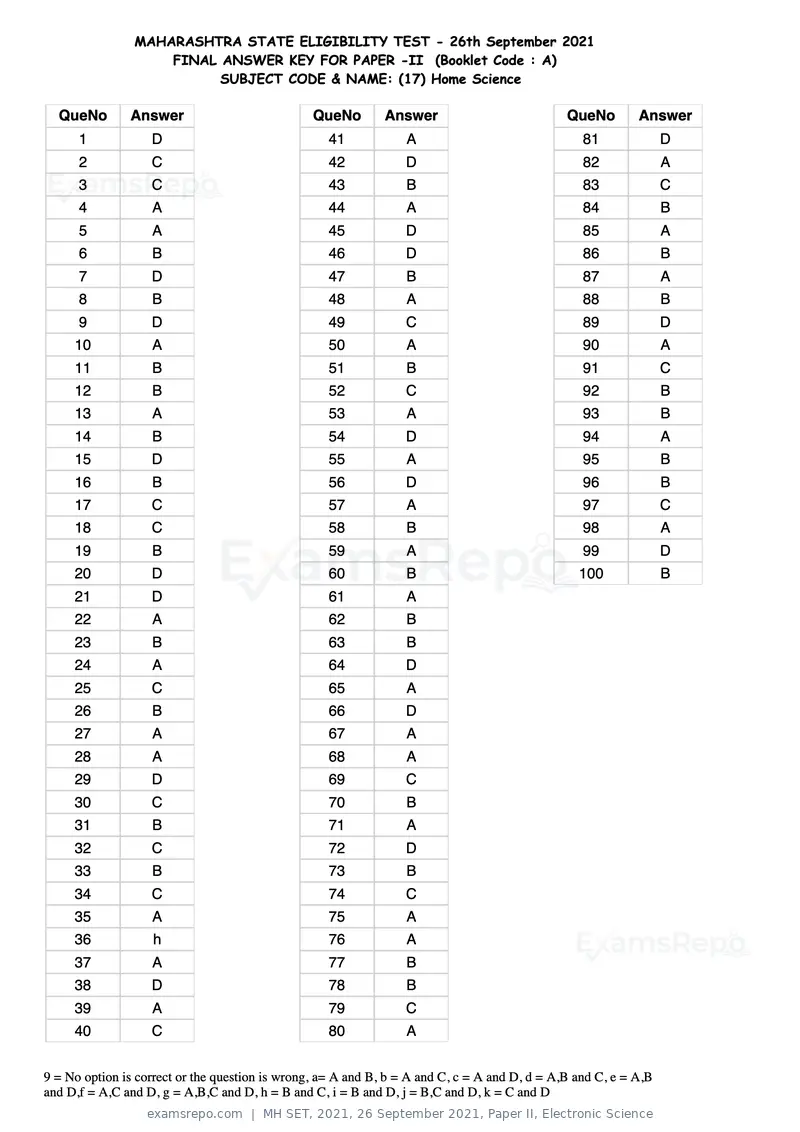
Text of page 49
MAHARASHTRA STATE ELIGIBILITY TEST - 26th September 2021
                    FINAL ANSWER KEY FOR PAPER -II (Booklet Code : A)
                          SUBJECT CODE & NAME: (17) Home Science

  QueNo        Answer                            QueNo        Answer                           QueNo        Answer
      1            D                               41             A                               81              D
      2            C                               42             D                               82              A
      3            C                               43             B                               83              C
      4            A                               44             A                               84              B
      5            A                               45             D                               85              A
      6            B                               46             D                               86              B
      7            D                               47             B                               87              A
      8            B                               48             A                               88              B
      9            D                               49             C                               89              D
     10            A                               50             A                               90              A
     11            B                               51             B                               91              C
     12            B                               52             C                               92              B
     13            A                               53             A                               93              B
     14            B                               54             D                               94              A
     15            D                               55             A                               95              B
     16            B                               56             D                               96              B
     17            C                               57             A                               97              C
     18            C                               58             B                               98              A
     19            B                               59             A                               99              D
     20            D                               60             B                              100              B
     21            D                               61             A
     22            A                               62             B
     23            B                               63             B
     24            A                               64             D
     25            C                               65             A
     26            B                               66             D
     27            A                               67             A
     28            A                               68             A
     29            D                               69             C
     30            C                               70             B
     31            B                               71             A
     32            C                               72             D
     33            B                               73             B
     34            C                               74             C
     35            A                               75             A
     36            h                               76             A
     37            A                               77             B
     38            D                               78             B
     39            A                               79             C
     40            C                               80             A


9 = No option is correct or the question is wrong, a= A and B, b = A and C, c = A and D, d = A,B and C, e = A,B
and D,f = A,C and D, g = A,B,C and D, h = B and C, i = B and D, j = B,C and D, k = C and D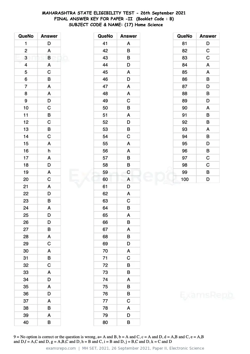
Text of page 50
MAHARASHTRA STATE ELIGIBILITY TEST - 26th September 2021
                    FINAL ANSWER KEY FOR PAPER -II (Booklet Code : B)
                         SUBJECT CODE & NAME: (17) Home Science

  QueNo        Answer                            QueNo        Answer                           QueNo        Answer
      1            D                               41             A                               81              D
      2            A                               42             B                               82              C
      3            B                               43             B                               83              C
      4            A                               44             D                               84              A
      5            C                               45             A                               85              A
      6            B                               46             D                               86              B
      7            A                               47             A                               87              D
      8            A                               48             A                               88              B
      9            D                               49             C                               89              D
     10            C                               50             B                               90              A
     11            B                               51             A                               91              B
     12            C                               52             D                               92              B
     13            B                               53             B                               93              A
     14            C                               54             C                               94              B
     15            A                               55             A                               95              D
     16            h                               56             A                               96              B
     17            A                               57             B                               97              C
     18            D                               58             B                               98              C
     19            A                               59             C                               99              B
     20            C                               60             A                              100              D
     21            A                               61             D
     22            D                               62             A
     23            B                               63             C
     24            A                               64             B
     25            D                               65             A
     26            D                               66             B
     27            B                               67             A
     28            A                               68             B
     29            C                               69             D
     30            A                               70             A
     31            B                               71             C
     32            C                               72             B
     33            A                               73             B
     34            D                               74             A
     35            A                               75             B
     36            D                               76             B
     37            A                               77             C
     38            B                               78             A
     39            A                               79             D
     40            B                               80             B


9 = No option is correct or the question is wrong, a= A and B, b = A and C, c = A and D, d = A,B and C, e = A,B
and D,f = A,C and D, g = A,B,C and D, h = B and C, i = B and D, j = B,C and D, k = C and D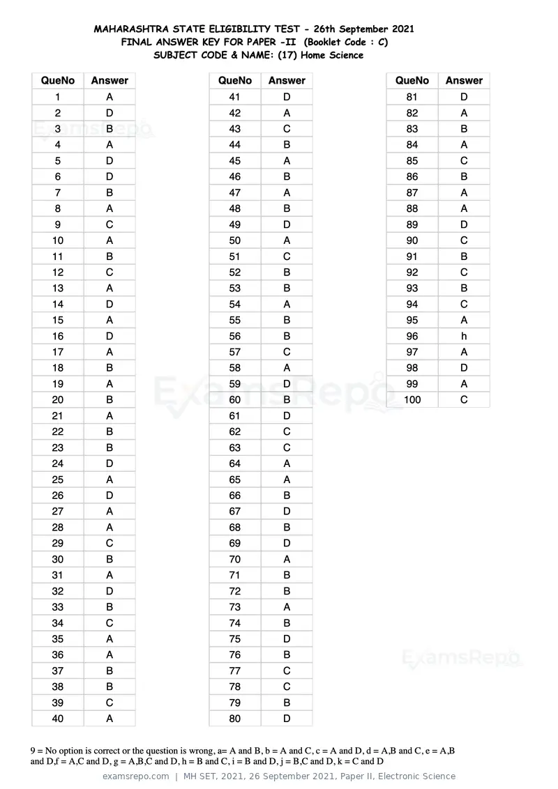
Text of page 51
MAHARASHTRA STATE ELIGIBILITY TEST - 26th September 2021
                    FINAL ANSWER KEY FOR PAPER -II (Booklet Code : C)
                         SUBJECT CODE & NAME: (17) Home Science

  QueNo        Answer                            QueNo        Answer                           QueNo        Answer
      1            A                               41             D                               81              D
      2            D                               42             A                               82              A
      3            B                               43             C                               83              B
      4            A                               44             B                               84              A
      5            D                               45             A                               85              C
      6            D                               46             B                               86              B
      7            B                               47             A                               87              A
      8            A                               48             B                               88              A
      9            C                               49             D                               89              D
     10            A                               50             A                               90              C
     11            B                               51             C                               91              B
     12            C                               52             B                               92              C
     13            A                               53             B                               93              B
     14            D                               54             A                               94              C
     15            A                               55             B                               95              A
     16            D                               56             B                               96              h
     17            A                               57             C                               97              A
     18            B                               58             A                               98              D
     19            A                               59             D                               99              A
     20            B                               60             B                              100              C
     21            A                               61             D
     22            B                               62             C
     23            B                               63             C
     24            D                               64             A
     25            A                               65             A
     26            D                               66             B
     27            A                               67             D
     28            A                               68             B
     29            C                               69             D
     30            B                               70             A
     31            A                               71             B
     32            D                               72             B
     33            B                               73             A
     34            C                               74             B
     35            A                               75             D
     36            A                               76             B
     37            B                               77             C
     38            B                               78             C
     39            C                               79             B
     40            A                               80             D


9 = No option is correct or the question is wrong, a= A and B, b = A and C, c = A and D, d = A,B and C, e = A,B
and D,f = A,C and D, g = A,B,C and D, h = B and C, i = B and D, j = B,C and D, k = C and D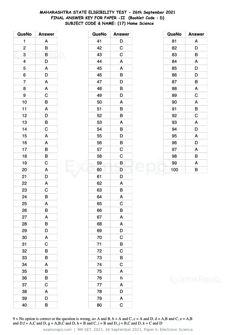
Text of page 52
MAHARASHTRA STATE ELIGIBILITY TEST - 26th September 2021
                    FINAL ANSWER KEY FOR PAPER -II (Booklet Code : D)
                          SUBJECT CODE & NAME: (17) Home Science

  QueNo        Answer                            QueNo        Answer                           QueNo        Answer
      1            A                               41             D                               81              A
      2            B                               42             C                               82              D
      3            B                               43             C                               83              B
      4            D                               44             A                               84              A
      5            A                               45             A                               85              D
      6            D                               46             B                               86              D
      7            A                               47             D                               87              B
      8            A                               48             B                               88              A
      9            C                               49             D                               89              C
     10            B                               50             A                               90              A
     11            A                               51             B                               91              B
     12            D                               52             B                               92              C
     13            B                               53             A                               93              A
     14            C                               54             B                               94              D
     15            A                               55             D                               95              A
     16            A                               56             B                               96              D
     17            B                               57             C                               97              A
     18            B                               58             C                               98              B
     19            C                               59             B                               99              A
     20            A                               60             D                              100              B
     21            D                               61             D
     22            A                               62             A
     23            C                               63             B
     24            B                               64             A
     25            A                               65             C
     26            B                               66             B
     27            A                               67             A
     28            B                               68             A
     29            D                               69             D
     30            A                               70             C
     31            C                               71             B
     32            B                               72             C
     33            B                               73             B
     34            A                               74             C
     35            B                               75             A
     36            B                               76             h
     37            C                               77             A
     38            A                               78             D
     39            D                               79             A
     40            B                               80             C


9 = No option is correct or the question is wrong, a= A and B, b = A and C, c = A and D, d = A,B and C, e = A,B
and D,f = A,C and D, g = A,B,C and D, h = B and C, i = B and D, j = B,C and D, k = C and D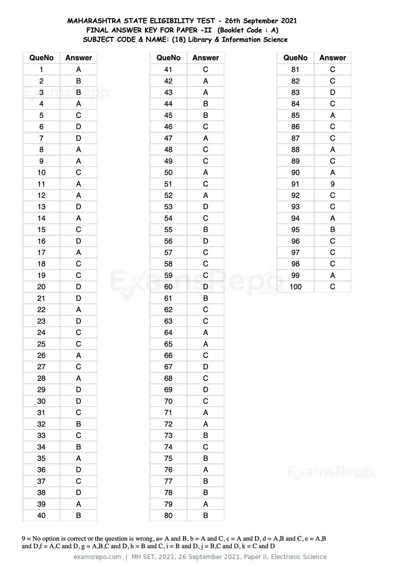
Text of page 53
MAHARASHTRA STATE ELIGIBILITY TEST - 26th September 2021
                    FINAL ANSWER KEY FOR PAPER -II (Booklet Code : A)
                   SUBJECT CODE & NAME: (18) Library & Information Science

  QueNo        Answer                            QueNo        Answer                           QueNo        Answer
      1            A                               41             C                               81              C
      2            B                               42             A                               82              C
      3            B                               43             A                               83              D
      4            A                               44             B                               84              C
      5            C                               45             B                               85              A
      6            D                               46             C                               86              C
      7            D                               47             A                               87              C
      8            A                               48             C                               88              A
      9            A                               49             C                               89              C
     10            C                               50             A                               90              A
     11            A                               51             C                               91              9
     12            A                               52             A                               92              C
     13            D                               53             D                               93              C
     14            A                               54             C                               94              A
     15            C                               55             B                               95              B
     16            D                               56             D                               96              C
     17            A                               57             C                               97              C
     18            C                               58             C                               98              C
     19            C                               59             C                               99              A
     20            D                               60             D                              100              C
     21            D                               61             B
     22            A                               62             C
     23            D                               63             C
     24            C                               64             A
     25            C                               65             A
     26            A                               66             C
     27            C                               67             D
     28            A                               68             C
     29            D                               69             D
     30            D                               70             C
     31            C                               71             A
     32            B                               72             A
     33            C                               73             B
     34            B                               74             C
     35            A                               75             B
     36            D                               76             A
     37            C                               77             B
     38            D                               78             B
     39            A                               79             A
     40            B                               80             B


9 = No option is correct or the question is wrong, a= A and B, b = A and C, c = A and D, d = A,B and C, e = A,B
and D,f = A,C and D, g = A,B,C and D, h = B and C, i = B and D, j = B,C and D, k = C and D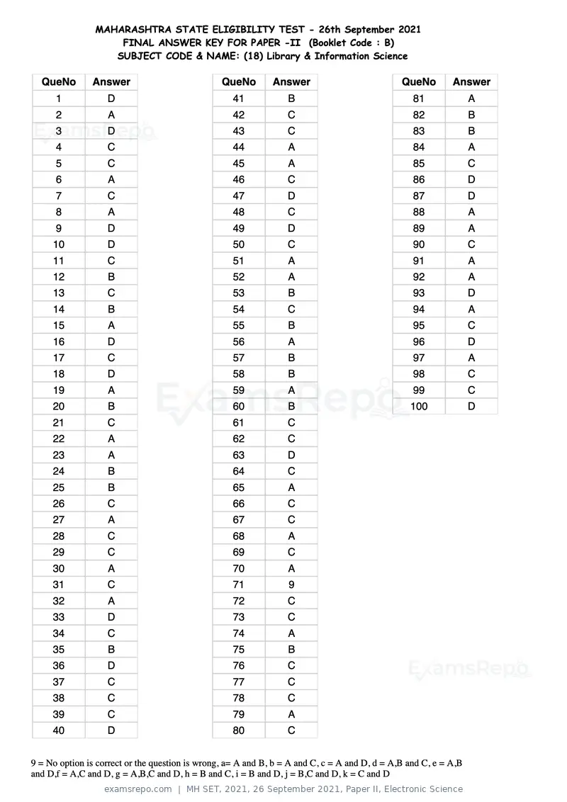
Text of page 54
MAHARASHTRA STATE ELIGIBILITY TEST - 26th September 2021
                    FINAL ANSWER KEY FOR PAPER -II (Booklet Code : B)
                   SUBJECT CODE & NAME: (18) Library & Information Science

  QueNo        Answer                            QueNo        Answer                           QueNo        Answer
      1            D                               41             B                               81              A
      2            A                               42             C                               82              B
      3            D                               43             C                               83              B
      4            C                               44             A                               84              A
      5            C                               45             A                               85              C
      6            A                               46             C                               86              D
      7            C                               47             D                               87              D
      8            A                               48             C                               88              A
      9            D                               49             D                               89              A
     10            D                               50             C                               90              C
     11            C                               51             A                               91              A
     12            B                               52             A                               92              A
     13            C                               53             B                               93              D
     14            B                               54             C                               94              A
     15            A                               55             B                               95              C
     16            D                               56             A                               96              D
     17            C                               57             B                               97              A
     18            D                               58             B                               98              C
     19            A                               59             A                               99              C
     20            B                               60             B                              100              D
     21            C                               61             C
     22            A                               62             C
     23            A                               63             D
     24            B                               64             C
     25            B                               65             A
     26            C                               66             C
     27            A                               67             C
     28            C                               68             A
     29            C                               69             C
     30            A                               70             A
     31            C                               71             9
     32            A                               72             C
     33            D                               73             C
     34            C                               74             A
     35            B                               75             B
     36            D                               76             C
     37            C                               77             C
     38            C                               78             C
     39            C                               79             A
     40            D                               80             C


9 = No option is correct or the question is wrong, a= A and B, b = A and C, c = A and D, d = A,B and C, e = A,B
and D,f = A,C and D, g = A,B,C and D, h = B and C, i = B and D, j = B,C and D, k = C and D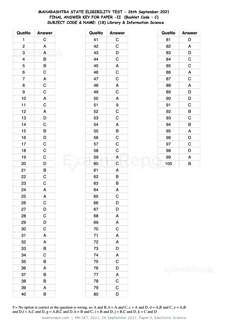
Text of page 55
MAHARASHTRA STATE ELIGIBILITY TEST - 26th September 2021
                    FINAL ANSWER KEY FOR PAPER -II (Booklet Code : C)
                   SUBJECT CODE & NAME: (18) Library & Information Science

  QueNo        Answer                            QueNo        Answer                           QueNo        Answer
      1            C                               41             C                               81              D
      2            A                               42             C                               82              A
      3            A                               43             D                               83              D
      4            B                               44             C                               84              C
      5            B                               45             A                               85              C
      6            C                               46             C                               86              A
      7            A                               47             C                               87              C
      8            C                               48             A                               88              A
      9            C                               49             C                               89              D
     10            A                               50             A                               90              D
     11            C                               51             9                               91              C
     12            A                               52             C                               92              B
     13            D                               53             C                               93              C
     14            C                               54             A                               94              B
     15            B                               55             B                               95              A
     16            D                               56             C                               96              D
     17            C                               57             C                               97              C
     18            C                               58             C                               98              D
     19            C                               59             A                               99              A
     20            D                               60             C                              100              B
     21            B                               61             A
     22            C                               62             B
     23            C                               63             B
     24            A                               64             A
     25            A                               65             C
     26            C                               66             D
     27            D                               67             D
     28            C                               68             A
     29            D                               69             A
     30            C                               70             C
     31            A                               71             A
     32            A                               72             A
     33            B                               73             D
     34            C                               74             A
     35            B                               75             C
     36            A                               76             D
     37            B                               77             A
     38            B                               78             C
     39            A                               79             C
     40            B                               80             D


9 = No option is correct or the question is wrong, a= A and B, b = A and C, c = A and D, d = A,B and C, e = A,B
and D,f = A,C and D, g = A,B,C and D, h = B and C, i = B and D, j = B,C and D, k = C and D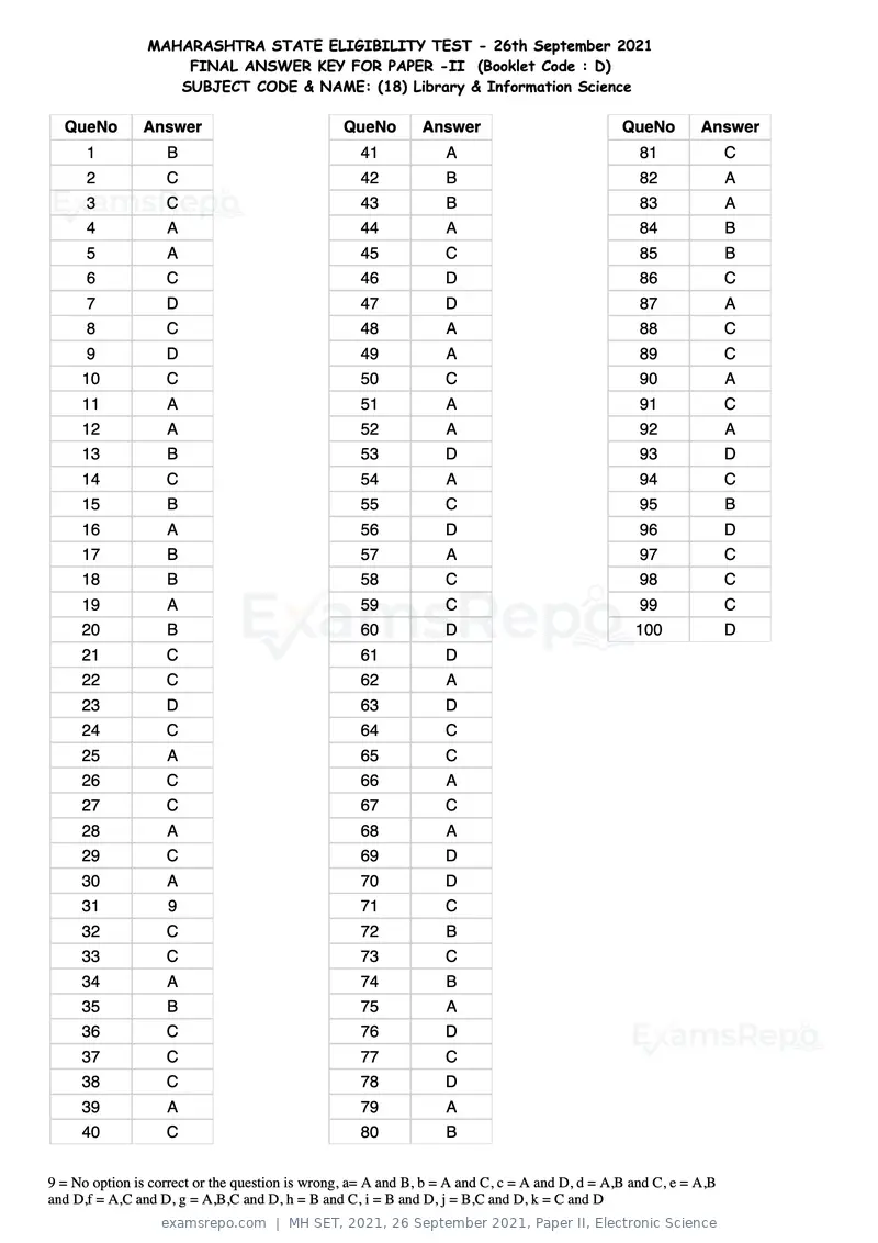
Text of page 56
MAHARASHTRA STATE ELIGIBILITY TEST - 26th September 2021
                    FINAL ANSWER KEY FOR PAPER -II (Booklet Code : D)
                   SUBJECT CODE & NAME: (18) Library & Information Science

  QueNo        Answer                            QueNo        Answer                           QueNo        Answer
      1            B                               41             A                               81              C
      2            C                               42             B                               82              A
      3            C                               43             B                               83              A
      4            A                               44             A                               84              B
      5            A                               45             C                               85              B
      6            C                               46             D                               86              C
      7            D                               47             D                               87              A
      8            C                               48             A                               88              C
      9            D                               49             A                               89              C
     10            C                               50             C                               90              A
     11            A                               51             A                               91              C
     12            A                               52             A                               92              A
     13            B                               53             D                               93              D
     14            C                               54             A                               94              C
     15            B                               55             C                               95              B
     16            A                               56             D                               96              D
     17            B                               57             A                               97              C
     18            B                               58             C                               98              C
     19            A                               59             C                               99              C
     20            B                               60             D                              100              D
     21            C                               61             D
     22            C                               62             A
     23            D                               63             D
     24            C                               64             C
     25            A                               65             C
     26            C                               66             A
     27            C                               67             C
     28            A                               68             A
     29            C                               69             D
     30            A                               70             D
     31            9                               71             C
     32            C                               72             B
     33            C                               73             C
     34            A                               74             B
     35            B                               75             A
     36            C                               76             D
     37            C                               77             C
     38            C                               78             D
     39            A                               79             A
     40            C                               80             B


9 = No option is correct or the question is wrong, a= A and B, b = A and C, c = A and D, d = A,B and C, e = A,B
and D,f = A,C and D, g = A,B,C and D, h = B and C, i = B and D, j = B,C and D, k = C and D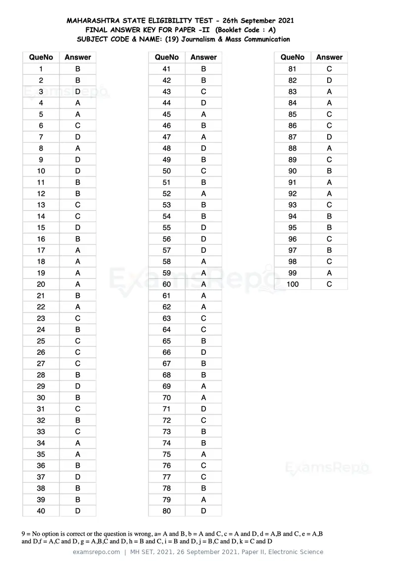
Text of page 57
MAHARASHTRA STATE ELIGIBILITY TEST - 26th September 2021
                    FINAL ANSWER KEY FOR PAPER -II (Booklet Code : A)
                  SUBJECT CODE & NAME: (19) Journalism & Mass Communication

  QueNo        Answer                            QueNo        Answer                           QueNo        Answer
      1            B                               41             B                               81              C
      2            B                               42             B                               82              D
      3            D                               43             C                               83              A
      4            A                               44             D                               84              A
      5            A                               45             A                               85              C
      6            C                               46             B                               86              C
      7            D                               47             A                               87              D
      8            A                               48             D                               88              A
      9            D                               49             B                               89              C
     10            D                               50             C                               90              B
     11            B                               51             B                               91              A
     12            B                               52             A                               92              A
     13            C                               53             B                               93              C
     14            C                               54             B                               94              B
     15            D                               55             D                               95              B
     16            B                               56             D                               96              C
     17            A                               57             D                               97              B
     18            A                               58             A                               98              C
     19            A                               59             A                               99              A
     20            A                               60             A                              100              C
     21            B                               61             A
     22            A                               62             A
     23            C                               63             C
     24            B                               64             C
     25            C                               65             B
     26            C                               66             D
     27            C                               67             B
     28            B                               68             B
     29            D                               69             A
     30            B                               70             A
     31            C                               71             D
     32            B                               72             C
     33            C                               73             B
     34            A                               74             B
     35            A                               75             A
     36            B                               76             C
     37            D                               77             C
     38            B                               78             B
     39            B                               79             A
     40            D                               80             D


9 = No option is correct or the question is wrong, a= A and B, b = A and C, c = A and D, d = A,B and C, e = A,B
and D,f = A,C and D, g = A,B,C and D, h = B and C, i = B and D, j = B,C and D, k = C and D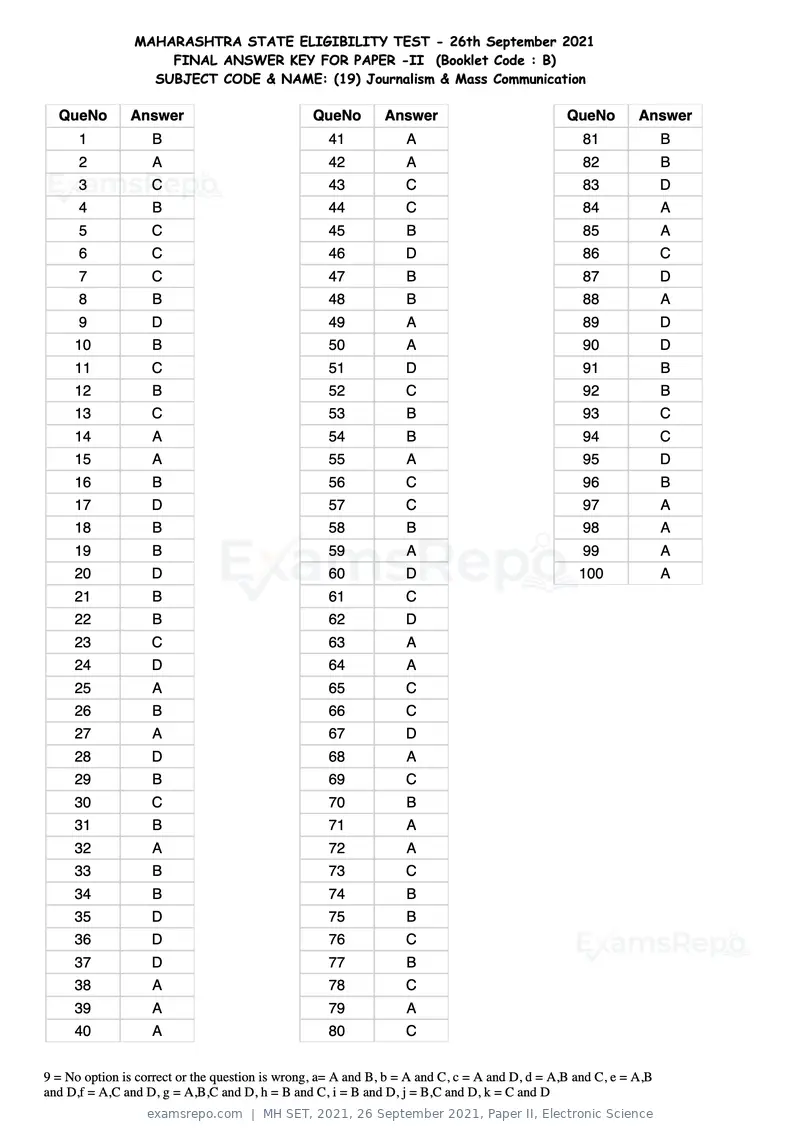
Text of page 58
MAHARASHTRA STATE ELIGIBILITY TEST - 26th September 2021
                    FINAL ANSWER KEY FOR PAPER -II (Booklet Code : B)
                  SUBJECT CODE & NAME: (19) Journalism & Mass Communication

  QueNo        Answer                            QueNo        Answer                           QueNo        Answer
      1            B                               41             A                               81              B
      2            A                               42             A                               82              B
      3            C                               43             C                               83              D
      4            B                               44             C                               84              A
      5            C                               45             B                               85              A
      6            C                               46             D                               86              C
      7            C                               47             B                               87              D
      8            B                               48             B                               88              A
      9            D                               49             A                               89              D
     10            B                               50             A                               90              D
     11            C                               51             D                               91              B
     12            B                               52             C                               92              B
     13            C                               53             B                               93              C
     14            A                               54             B                               94              C
     15            A                               55             A                               95              D
     16            B                               56             C                               96              B
     17            D                               57             C                               97              A
     18            B                               58             B                               98              A
     19            B                               59             A                               99              A
     20            D                               60             D                              100              A
     21            B                               61             C
     22            B                               62             D
     23            C                               63             A
     24            D                               64             A
     25            A                               65             C
     26            B                               66             C
     27            A                               67             D
     28            D                               68             A
     29            B                               69             C
     30            C                               70             B
     31            B                               71             A
     32            A                               72             A
     33            B                               73             C
     34            B                               74             B
     35            D                               75             B
     36            D                               76             C
     37            D                               77             B
     38            A                               78             C
     39            A                               79             A
     40            A                               80             C


9 = No option is correct or the question is wrong, a= A and B, b = A and C, c = A and D, d = A,B and C, e = A,B
and D,f = A,C and D, g = A,B,C and D, h = B and C, i = B and D, j = B,C and D, k = C and D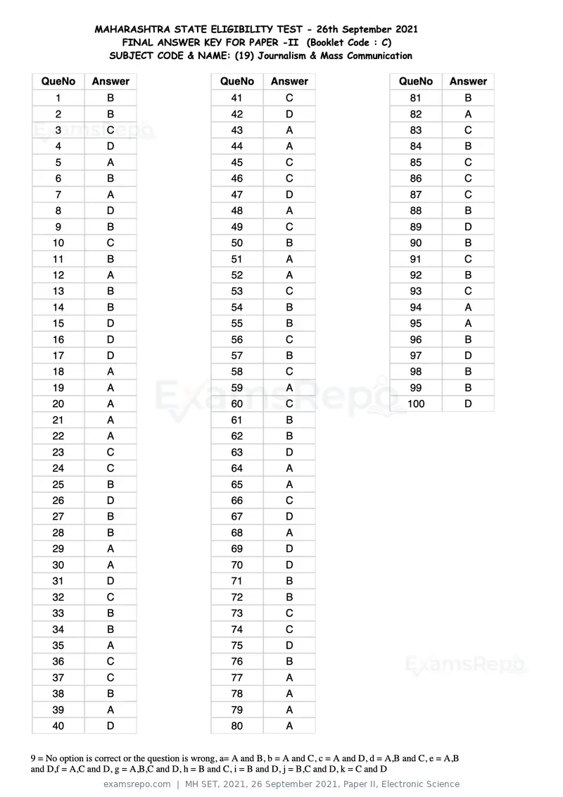
Text of page 59
MAHARASHTRA STATE ELIGIBILITY TEST - 26th September 2021
                    FINAL ANSWER KEY FOR PAPER -II (Booklet Code : C)
                  SUBJECT CODE & NAME: (19) Journalism & Mass Communication

  QueNo        Answer                            QueNo        Answer                           QueNo        Answer
      1            B                               41             C                               81              B
      2            B                               42             D                               82              A
      3            C                               43             A                               83              C
      4            D                               44             A                               84              B
      5            A                               45             C                               85              C
      6            B                               46             C                               86              C
      7            A                               47             D                               87              C
      8            D                               48             A                               88              B
      9            B                               49             C                               89              D
     10            C                               50             B                               90              B
     11            B                               51             A                               91              C
     12            A                               52             A                               92              B
     13            B                               53             C                               93              C
     14            B                               54             B                               94              A
     15            D                               55             B                               95              A
     16            D                               56             C                               96              B
     17            D                               57             B                               97              D
     18            A                               58             C                               98              B
     19            A                               59             A                               99              B
     20            A                               60             C                              100              D
     21            A                               61             B
     22            A                               62             B
     23            C                               63             D
     24            C                               64             A
     25            B                               65             A
     26            D                               66             C
     27            B                               67             D
     28            B                               68             A
     29            A                               69             D
     30            A                               70             D
     31            D                               71             B
     32            C                               72             B
     33            B                               73             C
     34            B                               74             C
     35            A                               75             D
     36            C                               76             B
     37            C                               77             A
     38            B                               78             A
     39            A                               79             A
     40            D                               80             A


9 = No option is correct or the question is wrong, a= A and B, b = A and C, c = A and D, d = A,B and C, e = A,B
and D,f = A,C and D, g = A,B,C and D, h = B and C, i = B and D, j = B,C and D, k = C and D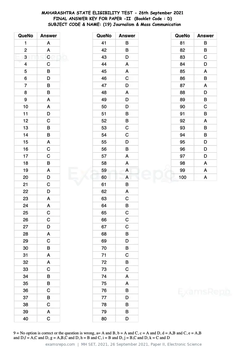
Text of page 60
MAHARASHTRA STATE ELIGIBILITY TEST - 26th September 2021
                    FINAL ANSWER KEY FOR PAPER -II (Booklet Code : D)
                  SUBJECT CODE & NAME: (19) Journalism & Mass Communication

  QueNo        Answer                            QueNo        Answer                           QueNo        Answer
      1            A                               41             B                               81              B
      2            A                               42             B                               82              B
      3            C                               43             D                               83              C
      4            C                               44             A                               84              D
      5            B                               45             A                               85              A
      6            D                               46             C                               86              B
      7            B                               47             D                               87              A
      8            B                               48             A                               88              D
      9            A                               49             D                               89              B
     10            A                               50             D                               90              C
     11            D                               51             B                               91              B
     12            C                               52             B                               92              A
     13            B                               53             C                               93              B
     14            B                               54             C                               94              B
     15            A                               55             D                               95              D
     16            C                               56             B                               96              D
     17            C                               57             A                               97              D
     18            B                               58             A                               98              A
     19            A                               59             A                               99              A
     20            D                               60             A                              100              A
     21            C                               61             B
     22            D                               62             A
     23            A                               63             C
     24            A                               64             B
     25            C                               65             C
     26            C                               66             C
     27            D                               67             C
     28            A                               68             B
     29            C                               69             D
     30            B                               70             B
     31            A                               71             C
     32            A                               72             B
     33            C                               73             C
     34            B                               74             A
     35            B                               75             A
     36            C                               76             B
     37            B                               77             D
     38            C                               78             B
     39            A                               79             B
     40            C                               80             D


9 = No option is correct or the question is wrong, a= A and B, b = A and C, c = A and D, d = A,B and C, e = A,B
and D,f = A,C and D, g = A,B,C and D, h = B and C, i = B and D, j = B,C and D, k = C and D
Text of page 61
MAHARASHTRA STATE ELIGIBILITY TEST - 26th September 2021
                    FINAL ANSWER KEY FOR PAPER -II (Booklet Code : A)
                          SUBJECT CODE & NAME: (20) Social Work

  QueNo        Answer                            QueNo        Answer                           QueNo        Answer
      1            D                               41             A                               81              C
      2            B                               42             A                               82              B
      3            A                               43             A                               83              C
      4            B                               44             A                               84              B
      5            B                               45             B                               85              C
      6            D                               46             C                               86              C
      7            A                               47             A                               87              B
      8            C                               48             D                               88              A
      9            C                               49             A                               89              C
     10            D                               50             A                               90              A
     11            A                               51             C                               91              C
     12            A                               52             C                               92              B
     13            A                               53             C                               93              C
     14            B                               54             C                               94              B
     15            C                               55             A                               95              B
     16            B                               56             B                               96              B
     17            B                               57             C                               97              B
     18            B                               58             A                               98              B
     19            C                               59             C                               99              A
     20            D                               60             A                              100              A
     21            A                               61             B
     22            B                               62             B
     23            B                               63             D
     24            A                               64             A
     25            A                               65             D
     26            D                               66             B
     27            C                               67             B
     28            B                               68             A
     29            C                               69             A
     30            C                               70             B
     31            D                               71             C
     32            B                               72             A
     33            D                               73             D
     34            B                               74             A
     35            C                               75             D
     36            B                               76             B
     37            A                               77             B
     38            A                               78             C
     39            D                               79             A
     40            A                               80             B


9 = No option is correct or the question is wrong, a= A and B, b = A and C, c = A and D, d = A,B and C, e = A,B
and D,f = A,C and D, g = A,B,C and D, h = B and C, i = B and D, j = B,C and D, k = C and D
Text of page 62
MAHARASHTRA STATE ELIGIBILITY TEST - 26th September 2021
                    FINAL ANSWER KEY FOR PAPER -II (Booklet Code : B)
                          SUBJECT CODE & NAME: (20) Social Work

  QueNo        Answer                            QueNo        Answer                           QueNo        Answer
      1            A                               41             B                               81              D
      2            B                               42             B                               82              B
      3            B                               43             D                               83              A
      4            A                               44             A                               84              B
      5            A                               45             D                               85              B
      6            D                               46             B                               86              D
      7            C                               47             B                               87              A
      8            B                               48             A                               88              C
      9            C                               49             A                               89              C
     10            C                               50             B                               90              D
     11            D                               51             C                               91              A
     12            B                               52             A                               92              A
     13            D                               53             D                               93              A
     14            B                               54             A                               94              B
     15            C                               55             D                               95              C
     16            B                               56             B                               96              B
     17            A                               57             B                               97              B
     18            A                               58             C                               98              B
     19            D                               59             A                               99              C
     20            A                               60             B                              100              D
     21            A                               61             C
     22            A                               62             B
     23            A                               63             C
     24            A                               64             B
     25            B                               65             C
     26            C                               66             C
     27            A                               67             B
     28            D                               68             A
     29            A                               69             C
     30            A                               70             A
     31            C                               71             C
     32            C                               72             B
     33            C                               73             C
     34            C                               74             B
     35            A                               75             B
     36            B                               76             B
     37            C                               77             B
     38            A                               78             B
     39            C                               79             A
     40            A                               80             A


9 = No option is correct or the question is wrong, a= A and B, b = A and C, c = A and D, d = A,B and C, e = A,B
and D,f = A,C and D, g = A,B,C and D, h = B and C, i = B and D, j = B,C and D, k = C and D
Text of page 63
MAHARASHTRA STATE ELIGIBILITY TEST - 26th September 2021
                    FINAL ANSWER KEY FOR PAPER -II (Booklet Code : C)
                          SUBJECT CODE & NAME: (20) Social Work

  QueNo        Answer                            QueNo        Answer                           QueNo        Answer
      1            A                               41             C                               81              A
      2            A                               42             B                               82              B
      3            A                               43             C                               83              B
      4            A                               44             B                               84              A
      5            B                               45             C                               85              A
      6            C                               46             C                               86              D
      7            A                               47             B                               87              C
      8            D                               48             A                               88              B
      9            A                               49             C                               89              C
     10            A                               50             A                               90              C
     11            C                               51             C                               91              D
     12            C                               52             B                               92              B
     13            C                               53             C                               93              D
     14            C                               54             B                               94              B
     15            A                               55             B                               95              C
     16            B                               56             B                               96              B
     17            C                               57             B                               97              A
     18            A                               58             B                               98              A
     19            C                               59             A                               99              D
     20            A                               60             A                              100              A
     21            B                               61             D
     22            B                               62             B
     23            D                               63             A
     24            A                               64             B
     25            D                               65             B
     26            B                               66             D
     27            B                               67             A
     28            A                               68             C
     29            A                               69             C
     30            B                               70             D
     31            C                               71             A
     32            A                               72             A
     33            D                               73             A
     34            A                               74             B
     35            D                               75             C
     36            B                               76             B
     37            B                               77             B
     38            C                               78             B
     39            A                               79             C
     40            B                               80             D


9 = No option is correct or the question is wrong, a= A and B, b = A and C, c = A and D, d = A,B and C, e = A,B
and D,f = A,C and D, g = A,B,C and D, h = B and C, i = B and D, j = B,C and D, k = C and D
Text of page 64
MAHARASHTRA STATE ELIGIBILITY TEST - 26th September 2021
                    FINAL ANSWER KEY FOR PAPER -II (Booklet Code : D)
                          SUBJECT CODE & NAME: (20) Social Work

  QueNo        Answer                            QueNo        Answer                           QueNo        Answer
      1            B                               41             D                               81              A
      2            B                               42             B                               82              A
      3            D                               43             A                               83              A
      4            A                               44             B                               84              A
      5            D                               45             B                               85              B
      6            B                               46             D                               86              C
      7            B                               47             A                               87              A
      8            A                               48             C                               88              D
      9            A                               49             C                               89              A
     10            B                               50             D                               90              A
     11            C                               51             A                               91              C
     12            A                               52             A                               92              C
     13            D                               53             A                               93              C
     14            A                               54             B                               94              C
     15            D                               55             C                               95              A
     16            B                               56             B                               96              B
     17            B                               57             B                               97              C
     18            C                               58             B                               98              A
     19            A                               59             C                               99              C
     20            B                               60             D                              100              A
     21            C                               61             A
     22            B                               62             B
     23            C                               63             B
     24            B                               64             A
     25            C                               65             A
     26            C                               66             D
     27            B                               67             C
     28            A                               68             B
     29            C                               69             C
     30            A                               70             C
     31            C                               71             D
     32            B                               72             B
     33            C                               73             D
     34            B                               74             B
     35            B                               75             C
     36            B                               76             B
     37            B                               77             A
     38            B                               78             A
     39            A                               79             D
     40            A                               80             A


9 = No option is correct or the question is wrong, a= A and B, b = A and C, c = A and D, d = A,B and C, e = A,B
and D,f = A,C and D, g = A,B,C and D, h = B and C, i = B and D, j = B,C and D, k = C and D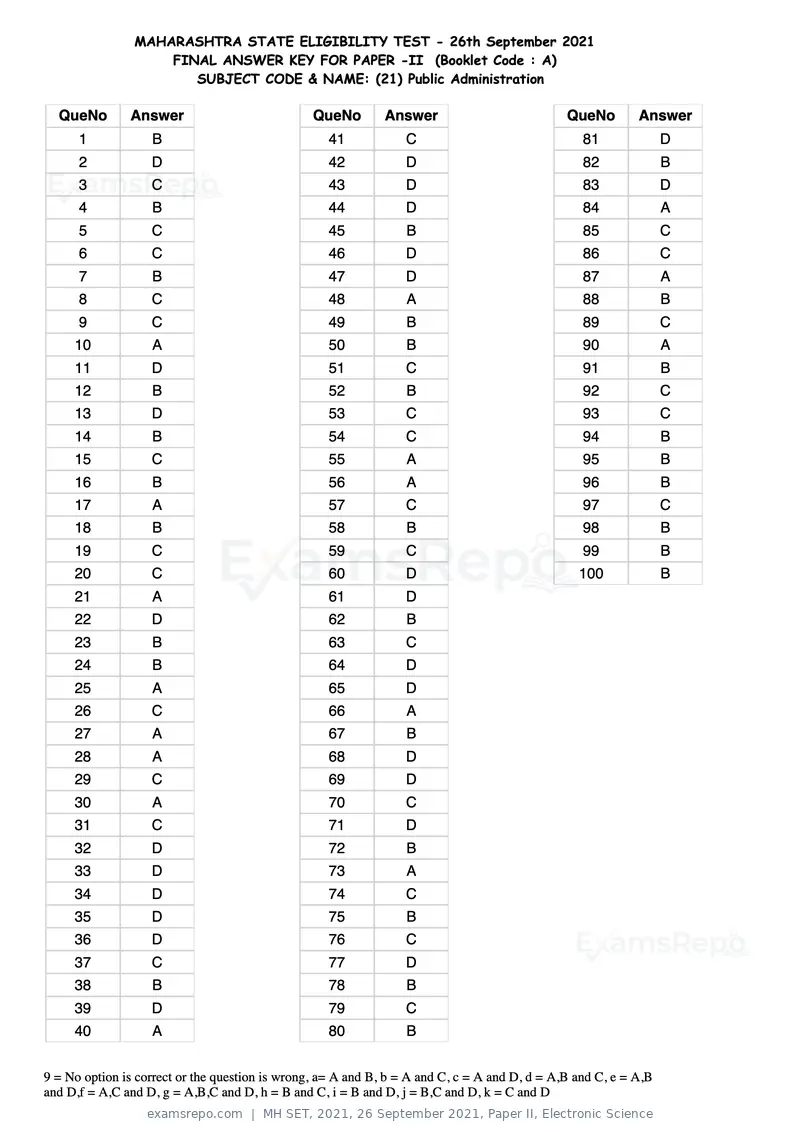
Text of page 65
MAHARASHTRA STATE ELIGIBILITY TEST - 26th September 2021
                    FINAL ANSWER KEY FOR PAPER -II (Booklet Code : A)
                       SUBJECT CODE & NAME: (21) Public Administration

  QueNo        Answer                            QueNo        Answer                           QueNo        Answer
      1            B                               41             C                               81              D
      2            D                               42             D                               82              B
      3            C                               43             D                               83              D
      4            B                               44             D                               84              A
      5            C                               45             B                               85              C
      6            C                               46             D                               86              C
      7            B                               47             D                               87              A
      8            C                               48             A                               88              B
      9            C                               49             B                               89              C
     10            A                               50             B                               90              A
     11            D                               51             C                               91              B
     12            B                               52             B                               92              C
     13            D                               53             C                               93              C
     14            B                               54             C                               94              B
     15            C                               55             A                               95              B
     16            B                               56             A                               96              B
     17            A                               57             C                               97              C
     18            B                               58             B                               98              B
     19            C                               59             C                               99              B
     20            C                               60             D                              100              B
     21            A                               61             D
     22            D                               62             B
     23            B                               63             C
     24            B                               64             D
     25            A                               65             D
     26            C                               66             A
     27            A                               67             B
     28            A                               68             D
     29            C                               69             D
     30            A                               70             C
     31            C                               71             D
     32            D                               72             B
     33            D                               73             A
     34            D                               74             C
     35            D                               75             B
     36            D                               76             C
     37            C                               77             D
     38            B                               78             B
     39            D                               79             C
     40            A                               80             B


9 = No option is correct or the question is wrong, a= A and B, b = A and C, c = A and D, d = A,B and C, e = A,B
and D,f = A,C and D, g = A,B,C and D, h = B and C, i = B and D, j = B,C and D, k = C and D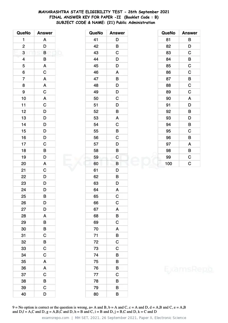
Text of page 66
MAHARASHTRA STATE ELIGIBILITY TEST - 26th September 2021
                    FINAL ANSWER KEY FOR PAPER -II (Booklet Code : B)
                       SUBJECT CODE & NAME: (21) Public Administration

  QueNo        Answer                            QueNo        Answer                           QueNo        Answer
      1            A                               41             D                               81              B
      2            D                               42             B                               82              D
      3            B                               43             C                               83              C
      4            B                               44             D                               84              B
      5            A                               45             D                               85              C
      6            C                               46             A                               86              C
      7            A                               47             B                               87              B
      8            A                               48             D                               88              C
      9            C                               49             D                               89              C
     10            A                               50             C                               90              A
     11            C                               51             D                               91              D
     12            D                               52             B                               92              B
     13            D                               53             A                               93              D
     14            D                               54             C                               94              B
     15            D                               55             B                               95              C
     16            D                               56             C                               96              B
     17            C                               57             D                               97              A
     18            B                               58             B                               98              B
     19            D                               59             C                               99              C
     20            A                               60             B                              100              C
     21            C                               61             D
     22            D                               62             B
     23            D                               63             D
     24            D                               64             A
     25            B                               65             C
     26            D                               66             C
     27            D                               67             A
     28            A                               68             B
     29            B                               69             C
     30            B                               70             A
     31            C                               71             B
     32            B                               72             C
     33            C                               73             C
     34            C                               74             B
     35            A                               75             B
     36            A                               76             B
     37            C                               77             C
     38            B                               78             B
     39            C                               79             B
     40            D                               80             B


9 = No option is correct or the question is wrong, a= A and B, b = A and C, c = A and D, d = A,B and C, e = A,B
and D,f = A,C and D, g = A,B,C and D, h = B and C, i = B and D, j = B,C and D, k = C and D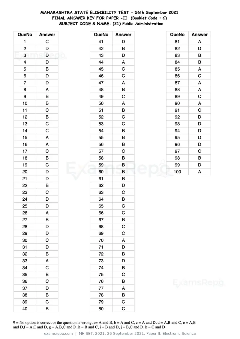
Text of page 67
MAHARASHTRA STATE ELIGIBILITY TEST - 26th September 2021
                    FINAL ANSWER KEY FOR PAPER -II (Booklet Code : C)
                       SUBJECT CODE & NAME: (21) Public Administration

  QueNo        Answer                            QueNo        Answer                           QueNo        Answer
      1            C                               41             D                               81              A
      2            D                               42             B                               82              D
      3            D                               43             D                               83              B
      4            D                               44             A                               84              B
      5            B                               45             C                               85              A
      6            D                               46             C                               86              C
      7            D                               47             A                               87              A
      8            A                               48             B                               88              A
      9            B                               49             C                               89              C
     10            B                               50             A                               90              A
     11            C                               51             B                               91              C
     12            B                               52             C                               92              D
     13            C                               53             C                               93              D
     14            C                               54             B                               94              D
     15            A                               55             B                               95              D
     16            A                               56             B                               96              D
     17            C                               57             C                               97              C
     18            B                               58             B                               98              B
     19            C                               59             B                               99              D
     20            D                               60             B                              100              A
     21            D                               61             B
     22            B                               62             D
     23            C                               63             C
     24            D                               64             B
     25            D                               65             C
     26            A                               66             C
     27            B                               67             B
     28            D                               68             C
     29            D                               69             C
     30            C                               70             A
     31            D                               71             D
     32            B                               72             B
     33            A                               73             D
     34            C                               74             B
     35            B                               75             C
     36            C                               76             B
     37            D                               77             A
     38            B                               78             B
     39            C                               79             C
     40            B                               80             C


9 = No option is correct or the question is wrong, a= A and B, b = A and C, c = A and D, d = A,B and C, e = A,B
and D,f = A,C and D, g = A,B,C and D, h = B and C, i = B and D, j = B,C and D, k = C and D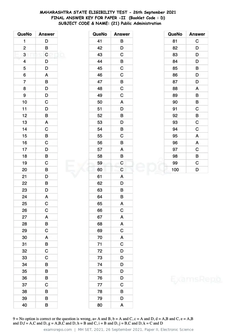
Text of page 68
MAHARASHTRA STATE ELIGIBILITY TEST - 26th September 2021
                    FINAL ANSWER KEY FOR PAPER -II (Booklet Code : D)
                       SUBJECT CODE & NAME: (21) Public Administration

  QueNo        Answer                            QueNo        Answer                           QueNo        Answer
      1            D                               41             B                               81              C
      2            B                               42             D                               82              D
      3            C                               43             C                               83              D
      4            D                               44             B                               84              D
      5            D                               45             C                               85              B
      6            A                               46             C                               86              D
      7            B                               47             B                               87              D
      8            D                               48             C                               88              A
      9            D                               49             C                               89              B
     10            C                               50             A                               90              B
     11            D                               51             D                               91              C
     12            B                               52             B                               92              B
     13            A                               53             D                               93              C
     14            C                               54             B                               94              C
     15            B                               55             C                               95              A
     16            C                               56             B                               96              A
     17            D                               57             A                               97              C
     18            B                               58             B                               98              B
     19            C                               59             C                               99              C
     20            B                               60             C                              100              D
     21            D                               61             A
     22            B                               62             D
     23            D                               63             B
     24            A                               64             B
     25            C                               65             A
     26            C                               66             C
     27            A                               67             A
     28            B                               68             A
     29            C                               69             C
     30            A                               70             A
     31            B                               71             C
     32            C                               72             D
     33            C                               73             D
     34            B                               74             D
     35            B                               75             D
     36            B                               76             D
     37            C                               77             C
     38            B                               78             B
     39            B                               79             D
     40            B                               80             A


9 = No option is correct or the question is wrong, a= A and B, b = A and C, c = A and D, d = A,B and C, e = A,B
and D,f = A,C and D, g = A,B,C and D, h = B and C, i = B and D, j = B,C and D, k = C and D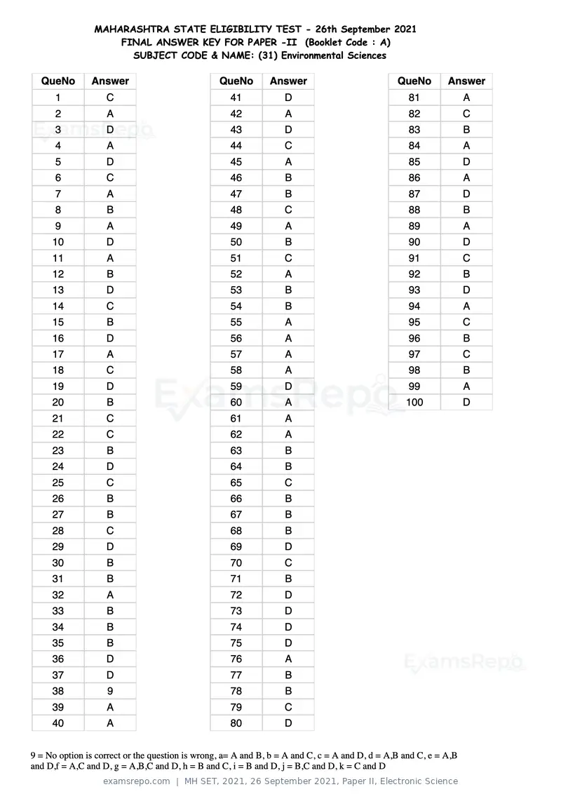
Text of page 69
MAHARASHTRA STATE ELIGIBILITY TEST - 26th September 2021
                    FINAL ANSWER KEY FOR PAPER -II (Booklet Code : A)
                      SUBJECT CODE & NAME: (31) Environmental Sciences

  QueNo        Answer                            QueNo        Answer                           QueNo        Answer
      1            C                               41             D                               81              A
      2            A                               42             A                               82              C
      3            D                               43             D                               83              B
      4            A                               44             C                               84              A
      5            D                               45             A                               85              D
      6            C                               46             B                               86              A
      7            A                               47             B                               87              D
      8            B                               48             C                               88              B
      9            A                               49             A                               89              A
     10            D                               50             B                               90              D
     11            A                               51             C                               91              C
     12            B                               52             A                               92              B
     13            D                               53             B                               93              D
     14            C                               54             B                               94              A
     15            B                               55             A                               95              C
     16            D                               56             A                               96              B
     17            A                               57             A                               97              C
     18            C                               58             A                               98              B
     19            D                               59             D                               99              A
     20            B                               60             A                              100              D
     21            C                               61             A
     22            C                               62             A
     23            B                               63             B
     24            D                               64             B
     25            C                               65             C
     26            B                               66             B
     27            B                               67             B
     28            C                               68             B
     29            D                               69             D
     30            B                               70             C
     31            B                               71             B
     32            A                               72             D
     33            B                               73             D
     34            B                               74             D
     35            B                               75             D
     36            D                               76             A
     37            D                               77             B
     38            9                               78             B
     39            A                               79             C
     40            A                               80             D


9 = No option is correct or the question is wrong, a= A and B, b = A and C, c = A and D, d = A,B and C, e = A,B
and D,f = A,C and D, g = A,B,C and D, h = B and C, i = B and D, j = B,C and D, k = C and D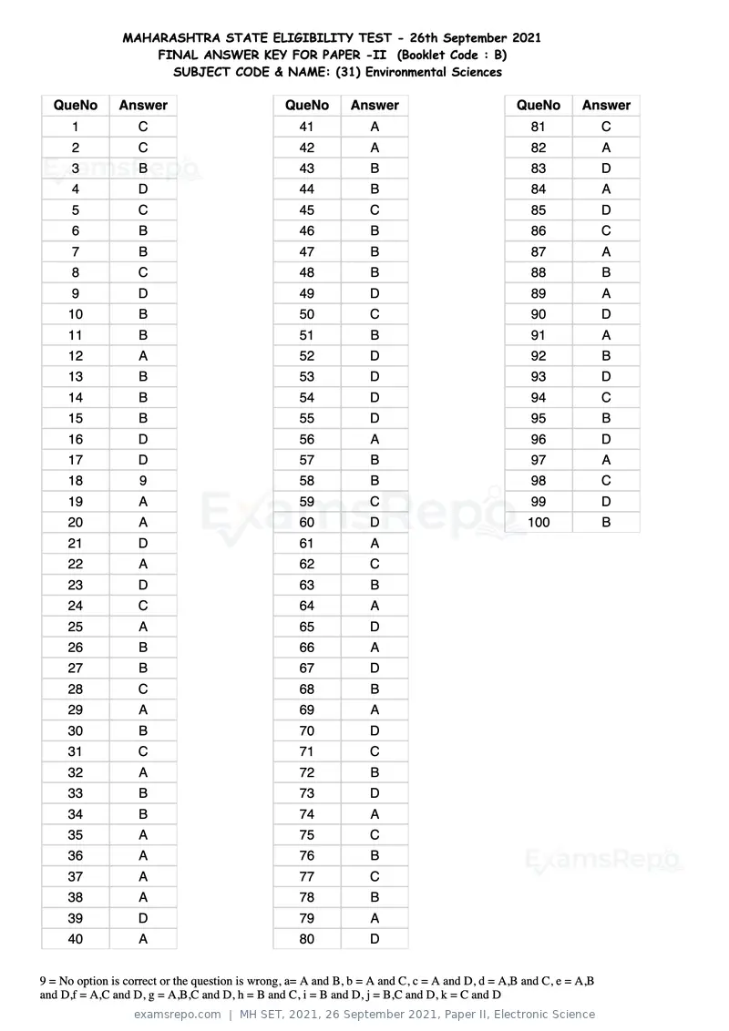
Text of page 70
MAHARASHTRA STATE ELIGIBILITY TEST - 26th September 2021
                    FINAL ANSWER KEY FOR PAPER -II (Booklet Code : B)
                      SUBJECT CODE & NAME: (31) Environmental Sciences

  QueNo        Answer                            QueNo        Answer                           QueNo        Answer
      1            C                               41             A                               81              C
      2            C                               42             A                               82              A
      3            B                               43             B                               83              D
      4            D                               44             B                               84              A
      5            C                               45             C                               85              D
      6            B                               46             B                               86              C
      7            B                               47             B                               87              A
      8            C                               48             B                               88              B
      9            D                               49             D                               89              A
     10            B                               50             C                               90              D
     11            B                               51             B                               91              A
     12            A                               52             D                               92              B
     13            B                               53             D                               93              D
     14            B                               54             D                               94              C
     15            B                               55             D                               95              B
     16            D                               56             A                               96              D
     17            D                               57             B                               97              A
     18            9                               58             B                               98              C
     19            A                               59             C                               99              D
     20            A                               60             D                              100              B
     21            D                               61             A
     22            A                               62             C
     23            D                               63             B
     24            C                               64             A
     25            A                               65             D
     26            B                               66             A
     27            B                               67             D
     28            C                               68             B
     29            A                               69             A
     30            B                               70             D
     31            C                               71             C
     32            A                               72             B
     33            B                               73             D
     34            B                               74             A
     35            A                               75             C
     36            A                               76             B
     37            A                               77             C
     38            A                               78             B
     39            D                               79             A
     40            A                               80             D


9 = No option is correct or the question is wrong, a= A and B, b = A and C, c = A and D, d = A,B and C, e = A,B
and D,f = A,C and D, g = A,B,C and D, h = B and C, i = B and D, j = B,C and D, k = C and D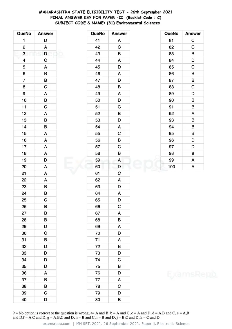
Text of page 71
MAHARASHTRA STATE ELIGIBILITY TEST - 26th September 2021
                    FINAL ANSWER KEY FOR PAPER -II (Booklet Code : C)
                      SUBJECT CODE & NAME: (31) Environmental Sciences

  QueNo        Answer                            QueNo        Answer                           QueNo        Answer
      1            D                               41             A                               81              C
      2            A                               42             C                               82              C
      3            D                               43             B                               83              B
      4            C                               44             A                               84              D
      5            A                               45             D                               85              C
      6            B                               46             A                               86              B
      7            B                               47             D                               87              B
      8            C                               48             B                               88              C
      9            A                               49             A                               89              D
     10            B                               50             D                               90              B
     11            C                               51             C                               91              B
     12            A                               52             B                               92              A
     13            B                               53             D                               93              B
     14            B                               54             A                               94              B
     15            A                               55             C                               95              B
     16            A                               56             B                               96              D
     17            A                               57             C                               97              D
     18            A                               58             B                               98              9
     19            D                               59             A                               99              A
     20            A                               60             D                              100              A
     21            A                               61             C
     22            A                               62             A
     23            B                               63             D
     24            B                               64             A
     25            C                               65             D
     26            B                               66             C
     27            B                               67             A
     28            B                               68             B
     29            D                               69             A
     30            C                               70             D
     31            B                               71             A
     32            D                               72             B
     33            D                               73             D
     34            D                               74             C
     35            D                               75             B
     36            A                               76             D
     37            B                               77             A
     38            B                               78             C
     39            C                               79             D
     40            D                               80             B


9 = No option is correct or the question is wrong, a= A and B, b = A and C, c = A and D, d = A,B and C, e = A,B
and D,f = A,C and D, g = A,B,C and D, h = B and C, i = B and D, j = B,C and D, k = C and D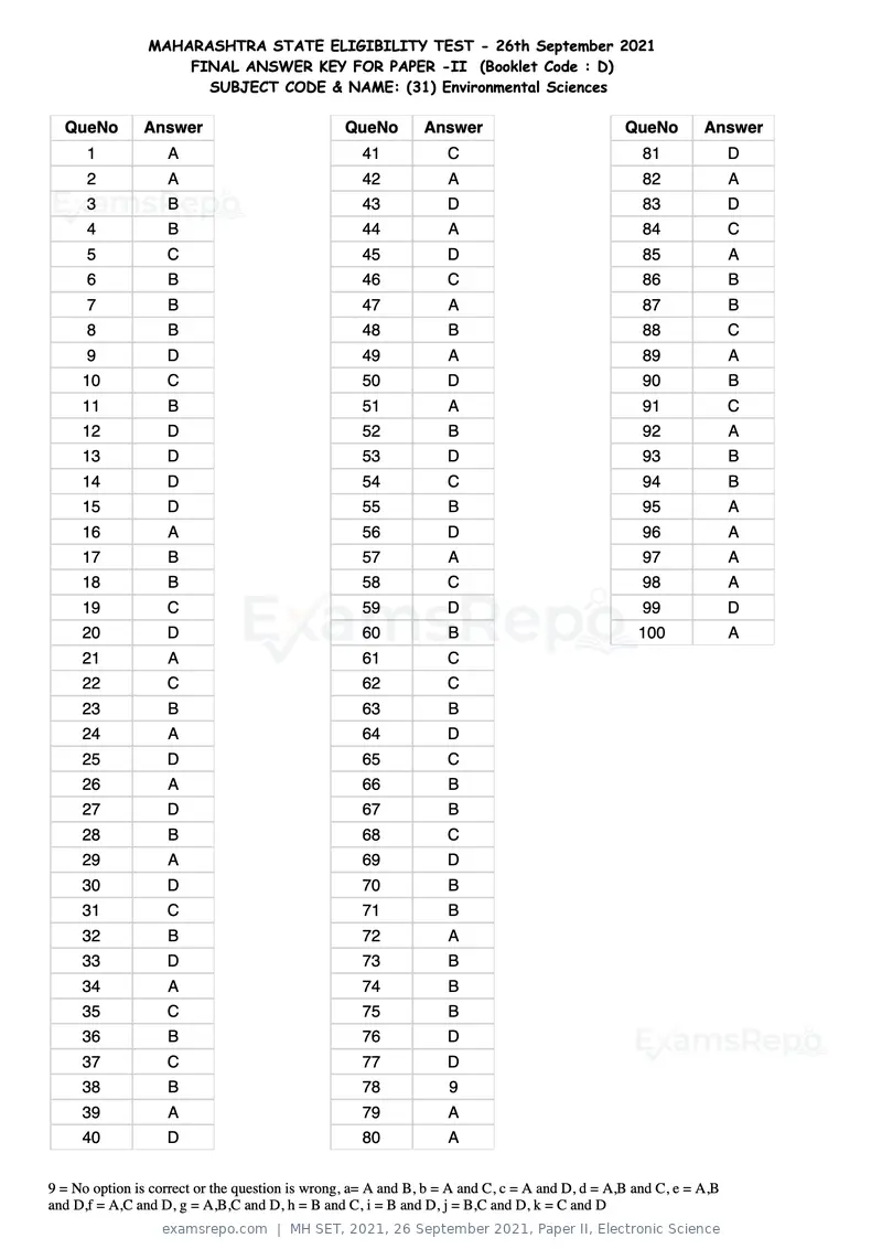
Text of page 72
MAHARASHTRA STATE ELIGIBILITY TEST - 26th September 2021
                    FINAL ANSWER KEY FOR PAPER -II (Booklet Code : D)
                      SUBJECT CODE & NAME: (31) Environmental Sciences

  QueNo        Answer                            QueNo        Answer                           QueNo        Answer
      1            A                               41             C                               81              D
      2            A                               42             A                               82              A
      3            B                               43             D                               83              D
      4            B                               44             A                               84              C
      5            C                               45             D                               85              A
      6            B                               46             C                               86              B
      7            B                               47             A                               87              B
      8            B                               48             B                               88              C
      9            D                               49             A                               89              A
     10            C                               50             D                               90              B
     11            B                               51             A                               91              C
     12            D                               52             B                               92              A
     13            D                               53             D                               93              B
     14            D                               54             C                               94              B
     15            D                               55             B                               95              A
     16            A                               56             D                               96              A
     17            B                               57             A                               97              A
     18            B                               58             C                               98              A
     19            C                               59             D                               99              D
     20            D                               60             B                              100              A
     21            A                               61             C
     22            C                               62             C
     23            B                               63             B
     24            A                               64             D
     25            D                               65             C
     26            A                               66             B
     27            D                               67             B
     28            B                               68             C
     29            A                               69             D
     30            D                               70             B
     31            C                               71             B
     32            B                               72             A
     33            D                               73             B
     34            A                               74             B
     35            C                               75             B
     36            B                               76             D
     37            C                               77             D
     38            B                               78             9
     39            A                               79             A
     40            D                               80             A


9 = No option is correct or the question is wrong, a= A and B, b = A and C, c = A and D, d = A,B and C, e = A,B
and D,f = A,C and D, g = A,B,C and D, h = B and C, i = B and D, j = B,C and D, k = C and D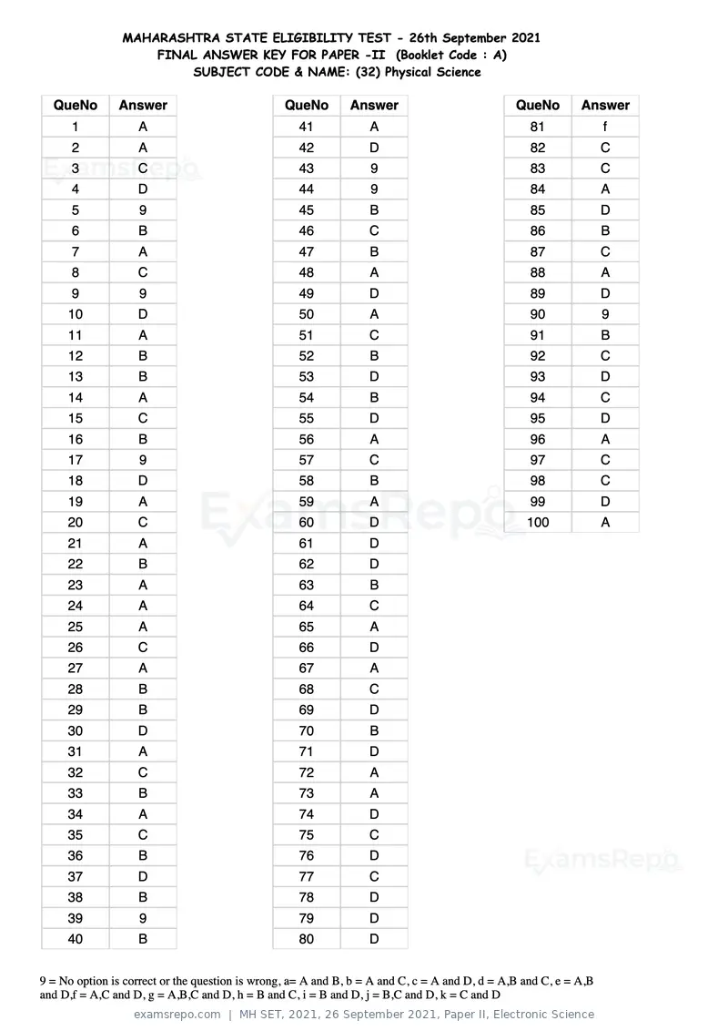
Text of page 73
MAHARASHTRA STATE ELIGIBILITY TEST - 26th September 2021
                    FINAL ANSWER KEY FOR PAPER -II (Booklet Code : A)
                        SUBJECT CODE & NAME: (32) Physical Science

  QueNo        Answer                            QueNo        Answer                           QueNo        Answer
      1            A                               41             A                               81              f
      2            A                               42             D                               82              C
      3            C                               43             9                               83              C
      4            D                               44             9                               84              A
      5            9                               45             B                               85              D
      6            B                               46             C                               86              B
      7            A                               47             B                               87              C
      8            C                               48             A                               88              A
      9            9                               49             D                               89              D
     10            D                               50             A                               90              9
     11            A                               51             C                               91              B
     12            B                               52             B                               92              C
     13            B                               53             D                               93              D
     14            A                               54             B                               94              C
     15            C                               55             D                               95              D
     16            B                               56             A                               96              A
     17            9                               57             C                               97              C
     18            D                               58             B                               98              C
     19            A                               59             A                               99              D
     20            C                               60             D                              100              A
     21            A                               61             D
     22            B                               62             D
     23            A                               63             B
     24            A                               64             C
     25            A                               65             A
     26            C                               66             D
     27            A                               67             A
     28            B                               68             C
     29            B                               69             D
     30            D                               70             B
     31            A                               71             D
     32            C                               72             A
     33            B                               73             A
     34            A                               74             D
     35            C                               75             C
     36            B                               76             D
     37            D                               77             C
     38            B                               78             D
     39            9                               79             D
     40            B                               80             D


9 = No option is correct or the question is wrong, a= A and B, b = A and C, c = A and D, d = A,B and C, e = A,B
and D,f = A,C and D, g = A,B,C and D, h = B and C, i = B and D, j = B,C and D, k = C and D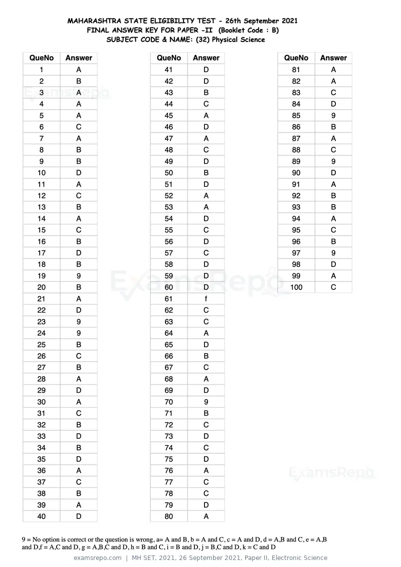
Text of page 74
MAHARASHTRA STATE ELIGIBILITY TEST - 26th September 2021
                    FINAL ANSWER KEY FOR PAPER -II (Booklet Code : B)
                        SUBJECT CODE & NAME: (32) Physical Science

  QueNo        Answer                            QueNo        Answer                           QueNo        Answer
      1            A                               41             D                               81              A
      2            B                               42             D                               82              A
      3            A                               43             B                               83              C
      4            A                               44             C                               84              D
      5            A                               45             A                               85              9
      6            C                               46             D                               86              B
      7            A                               47             A                               87              A
      8            B                               48             C                               88              C
      9            B                               49             D                               89              9
     10            D                               50             B                               90              D
     11            A                               51             D                               91              A
     12            C                               52             A                               92              B
     13            B                               53             A                               93              B
     14            A                               54             D                               94              A
     15            C                               55             C                               95              C
     16            B                               56             D                               96              B
     17            D                               57             C                               97              9
     18            B                               58             D                               98              D
     19            9                               59             D                               99              A
     20            B                               60             D                              100              C
     21            A                               61             f
     22            D                               62             C
     23            9                               63             C
     24            9                               64             A
     25            B                               65             D
     26            C                               66             B
     27            B                               67             C
     28            A                               68             A
     29            D                               69             D
     30            A                               70             9
     31            C                               71             B
     32            B                               72             C
     33            D                               73             D
     34            B                               74             C
     35            D                               75             D
     36            A                               76             A
     37            C                               77             C
     38            B                               78             C
     39            A                               79             D
     40            D                               80             A


9 = No option is correct or the question is wrong, a= A and B, b = A and C, c = A and D, d = A,B and C, e = A,B
and D,f = A,C and D, g = A,B,C and D, h = B and C, i = B and D, j = B,C and D, k = C and D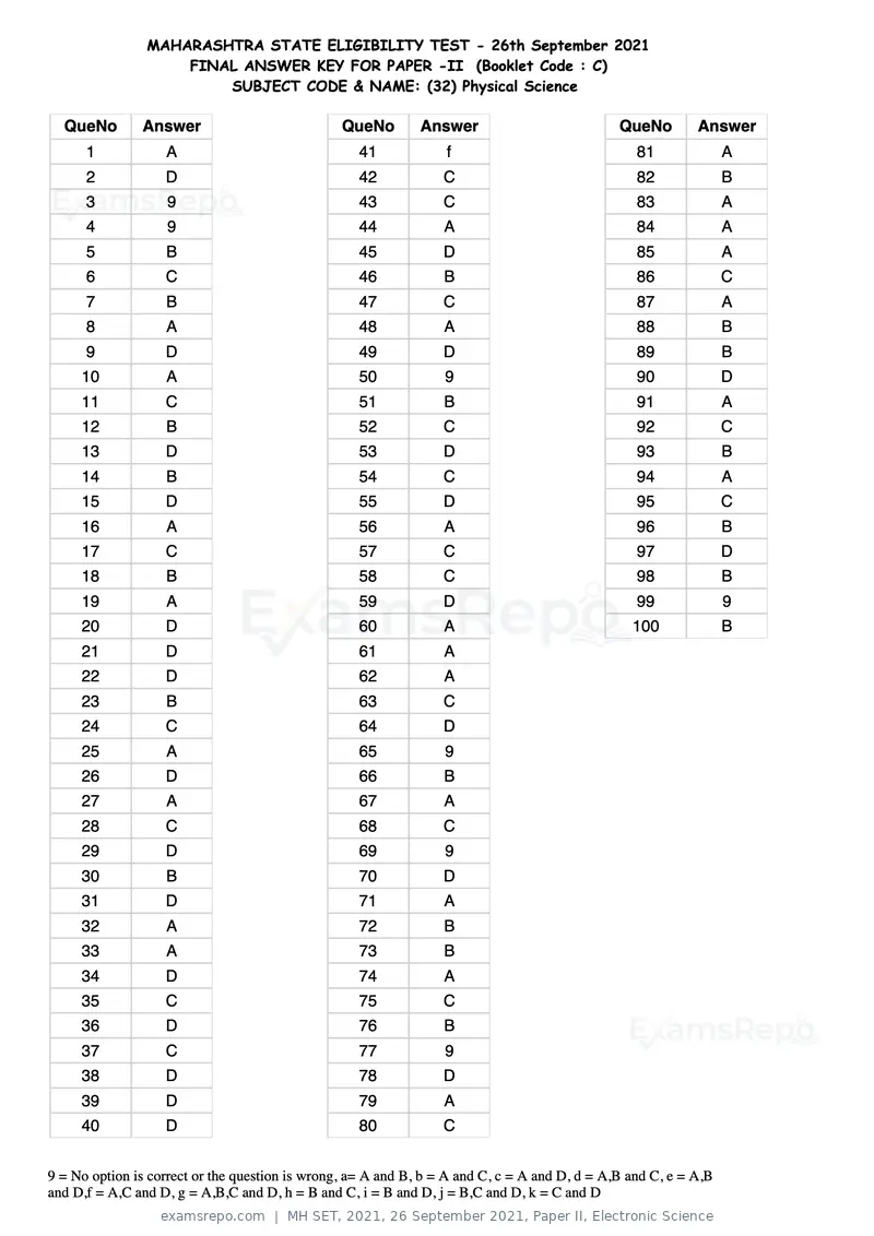
Text of page 75
MAHARASHTRA STATE ELIGIBILITY TEST - 26th September 2021
                    FINAL ANSWER KEY FOR PAPER -II (Booklet Code : C)
                        SUBJECT CODE & NAME: (32) Physical Science

  QueNo        Answer                            QueNo        Answer                           QueNo        Answer
      1            A                               41             f                               81              A
      2            D                               42             C                               82              B
      3            9                               43             C                               83              A
      4            9                               44             A                               84              A
      5            B                               45             D                               85              A
      6            C                               46             B                               86              C
      7            B                               47             C                               87              A
      8            A                               48             A                               88              B
      9            D                               49             D                               89              B
     10            A                               50             9                               90              D
     11            C                               51             B                               91              A
     12            B                               52             C                               92              C
     13            D                               53             D                               93              B
     14            B                               54             C                               94              A
     15            D                               55             D                               95              C
     16            A                               56             A                               96              B
     17            C                               57             C                               97              D
     18            B                               58             C                               98              B
     19            A                               59             D                               99              9
     20            D                               60             A                              100              B
     21            D                               61             A
     22            D                               62             A
     23            B                               63             C
     24            C                               64             D
     25            A                               65             9
     26            D                               66             B
     27            A                               67             A
     28            C                               68             C
     29            D                               69             9
     30            B                               70             D
     31            D                               71             A
     32            A                               72             B
     33            A                               73             B
     34            D                               74             A
     35            C                               75             C
     36            D                               76             B
     37            C                               77             9
     38            D                               78             D
     39            D                               79             A
     40            D                               80             C


9 = No option is correct or the question is wrong, a= A and B, b = A and C, c = A and D, d = A,B and C, e = A,B
and D,f = A,C and D, g = A,B,C and D, h = B and C, i = B and D, j = B,C and D, k = C and D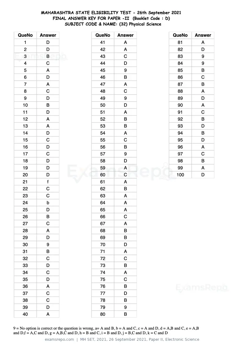
Text of page 76
MAHARASHTRA STATE ELIGIBILITY TEST - 26th September 2021
                    FINAL ANSWER KEY FOR PAPER -II (Booklet Code : D)
                        SUBJECT CODE & NAME: (32) Physical Science

  QueNo        Answer                            QueNo        Answer                           QueNo        Answer
      1            D                               41             A                               81              A
      2            D                               42             A                               82              D
      3            B                               43             C                               83              9
      4            C                               44             D                               84              9
      5            A                               45             9                               85              B
      6            D                               46             B                               86              C
      7            A                               47             A                               87              B
      8            C                               48             C                               88              A
      9            D                               49             9                               89              D
     10            B                               50             D                               90              A
     11            D                               51             A                               91              C
     12            A                               52             B                               92              B
     13            A                               53             B                               93              D
     14            D                               54             A                               94              B
     15            C                               55             C                               95              D
     16            D                               56             B                               96              A
     17            C                               57             9                               97              C
     18            D                               58             D                               98              B
     19            D                               59             A                               99              A
     20            D                               60             C                              100              D
     21             f                              61             A
     22            C                               62             B
     23            C                               63             A
     24            b                               64             A
     25            D                               65             A
     26            B                               66             C
     27            C                               67             A
     28            A                               68             B
     29            D                               69             B
     30            9                               70             D
     31            B                               71             A
     32            C                               72             C
     33            D                               73             B
     34            C                               74             A
     35            D                               75             C
     36            A                               76             B
     37            C                               77             D
     38            C                               78             B
     39            D                               79             9
     40            A                               80             B


9 = No option is correct or the question is wrong, a= A and B, b = A and C, c = A and D, d = A,B and C, e = A,B
and D,f = A,C and D, g = A,B,C and D, h = B and C, i = B and D, j = B,C and D, k = C and D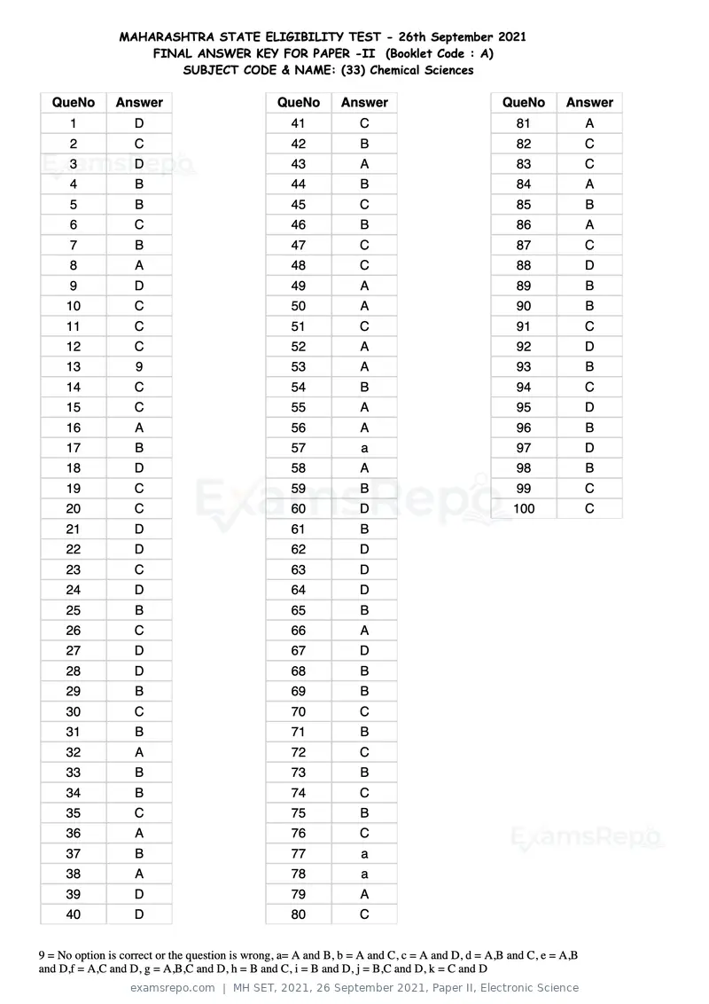
Text of page 77
MAHARASHTRA STATE ELIGIBILITY TEST - 26th September 2021
                    FINAL ANSWER KEY FOR PAPER -II (Booklet Code : A)
                        SUBJECT CODE & NAME: (33) Chemical Sciences

  QueNo        Answer                            QueNo        Answer                           QueNo        Answer
      1            D                               41             C                               81              A
      2            C                               42             B                               82              C
      3            D                               43             A                               83              C
      4            B                               44             B                               84              A
      5            B                               45             C                               85              B
      6            C                               46             B                               86              A
      7            B                               47             C                               87              C
      8            A                               48             C                               88              D
      9            D                               49             A                               89              B
     10            C                               50             A                               90              B
     11            C                               51             C                               91              C
     12            C                               52             A                               92              D
     13            9                               53             A                               93              B
     14            C                               54             B                               94              C
     15            C                               55             A                               95              D
     16            A                               56             A                               96              B
     17            B                               57             a                               97              D
     18            D                               58             A                               98              B
     19            C                               59             B                               99              C
     20            C                               60             D                              100              C
     21            D                               61             B
     22            D                               62             D
     23            C                               63             D
     24            D                               64             D
     25            B                               65             B
     26            C                               66             A
     27            D                               67             D
     28            D                               68             B
     29            B                               69             B
     30            C                               70             C
     31            B                               71             B
     32            A                               72             C
     33            B                               73             B
     34            B                               74             C
     35            C                               75             B
     36            A                               76             C
     37            B                               77             a
     38            A                               78             a
     39            D                               79             A
     40            D                               80             C


9 = No option is correct or the question is wrong, a= A and B, b = A and C, c = A and D, d = A,B and C, e = A,B
and D,f = A,C and D, g = A,B,C and D, h = B and C, i = B and D, j = B,C and D, k = C and D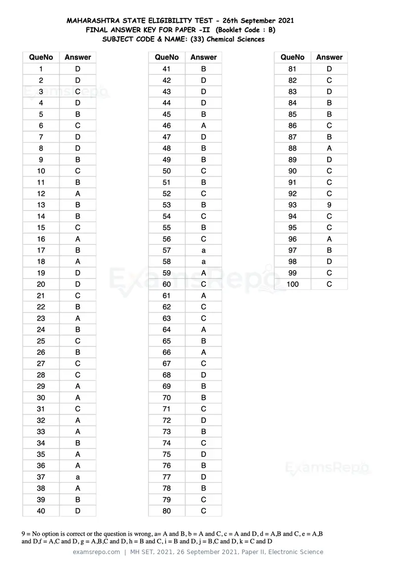
Text of page 78
MAHARASHTRA STATE ELIGIBILITY TEST - 26th September 2021
                    FINAL ANSWER KEY FOR PAPER -II (Booklet Code : B)
                        SUBJECT CODE & NAME: (33) Chemical Sciences

  QueNo        Answer                            QueNo        Answer                           QueNo        Answer
      1            D                               41             B                               81              D
      2            D                               42             D                               82              C
      3            C                               43             D                               83              D
      4            D                               44             D                               84              B
      5            B                               45             B                               85              B
      6            C                               46             A                               86              C
      7            D                               47             D                               87              B
      8            D                               48             B                               88              A
      9            B                               49             B                               89              D
     10            C                               50             C                               90              C
     11            B                               51             B                               91              C
     12            A                               52             C                               92              C
     13            B                               53             B                               93              9
     14            B                               54             C                               94              C
     15            C                               55             B                               95              C
     16            A                               56             C                               96              A
     17            B                               57             a                               97              B
     18            A                               58             a                               98              D
     19            D                               59             A                               99              C
     20            D                               60             C                              100              C
     21            C                               61             A
     22            B                               62             C
     23            A                               63             C
     24            B                               64             A
     25            C                               65             B
     26            B                               66             A
     27            C                               67             C
     28            C                               68             D
     29            A                               69             B
     30            A                               70             B
     31            C                               71             C
     32            A                               72             D
     33            A                               73             B
     34            B                               74             C
     35            A                               75             D
     36            A                               76             B
     37            a                               77             D
     38            A                               78             B
     39            B                               79             C
     40            D                               80             C


9 = No option is correct or the question is wrong, a= A and B, b = A and C, c = A and D, d = A,B and C, e = A,B
and D,f = A,C and D, g = A,B,C and D, h = B and C, i = B and D, j = B,C and D, k = C and D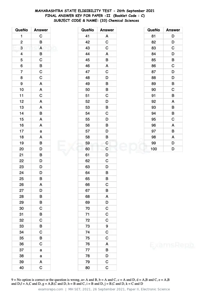
Text of page 79
MAHARASHTRA STATE ELIGIBILITY TEST - 26th September 2021
                    FINAL ANSWER KEY FOR PAPER -II (Booklet Code : C)
                        SUBJECT CODE & NAME: (33) Chemical Sciences

  QueNo        Answer                            QueNo        Answer                           QueNo        Answer
      1            C                               41             A                               81              D
      2            B                               42             C                               82              D
      3            A                               43             C                               83              C
      4            B                               44             A                               84              D
      5            C                               45             B                               85              B
      6            B                               46             A                               86              C
      7            C                               47             C                               87              D
      8            C                               48             D                               88              D
      9            A                               49             B                               89              B
     10            A                               50             B                               90              C
     11            C                               51             C                               91              B
     12            A                               52             D                               92              A
     13            A                               53             B                               93              B
     14            B                               54             C                               94              B
     15            A                               55             D                               95              C
     16            A                               56             B                               96              A
     17            a                               57             D                               97              B
     18            A                               58             B                               98              A
     19            B                               59             C                               99              D
     20            D                               60             C                              100              D
     21            B                               61             D
     22            D                               62             C
     23            D                               63             D
     24            D                               64             B
     25            B                               65             B
     26            A                               66             C
     27            D                               67             B
     28            B                               68             A
     29            B                               69             D
     30            C                               70             C
     31            B                               71             C
     32            C                               72             C
     33            B                               73             9
     34            C                               74             C
     35            B                               75             C
     36            C                               76             A
     37            a                               77             B
     38            a                               78             D
     39            A                               79             C
     40            C                               80             C


9 = No option is correct or the question is wrong, a= A and B, b = A and C, c = A and D, d = A,B and C, e = A,B
and D,f = A,C and D, g = A,B,C and D, h = B and C, i = B and D, j = B,C and D, k = C and D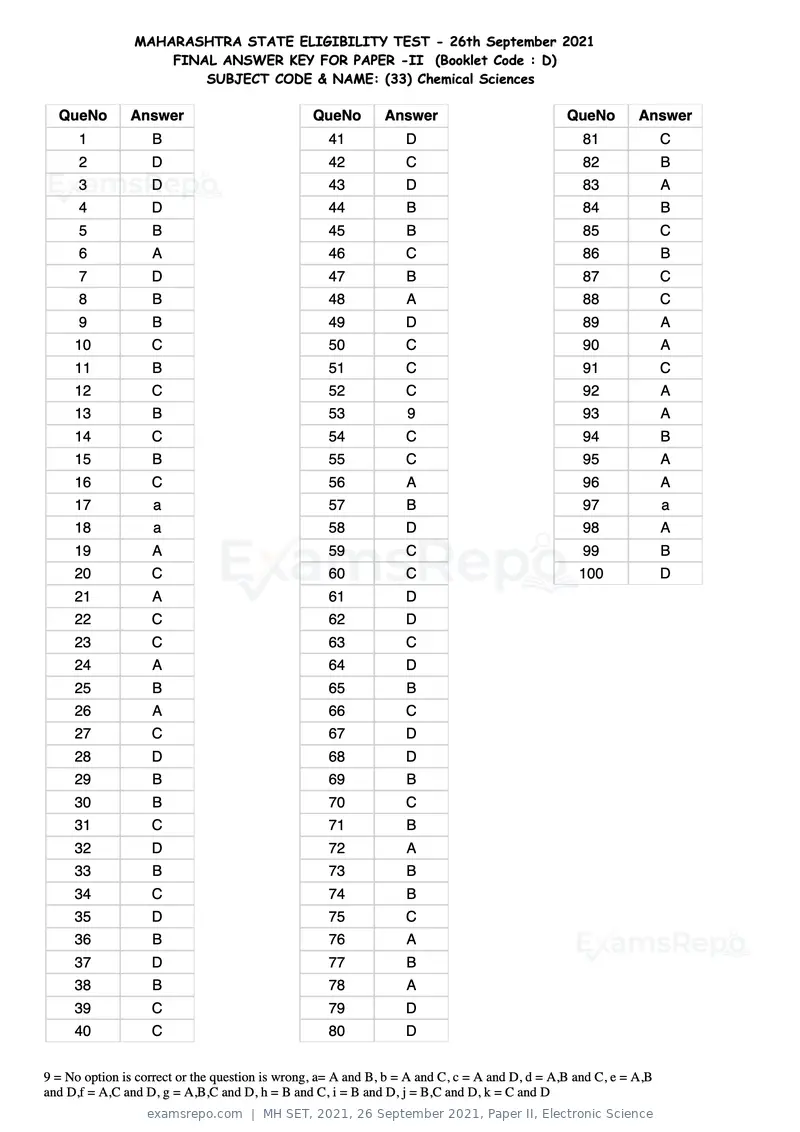
Text of page 80
MAHARASHTRA STATE ELIGIBILITY TEST - 26th September 2021
                    FINAL ANSWER KEY FOR PAPER -II (Booklet Code : D)
                        SUBJECT CODE & NAME: (33) Chemical Sciences

  QueNo        Answer                            QueNo        Answer                           QueNo        Answer
      1            B                               41             D                               81              C
      2            D                               42             C                               82              B
      3            D                               43             D                               83              A
      4            D                               44             B                               84              B
      5            B                               45             B                               85              C
      6            A                               46             C                               86              B
      7            D                               47             B                               87              C
      8            B                               48             A                               88              C
      9            B                               49             D                               89              A
     10            C                               50             C                               90              A
     11            B                               51             C                               91              C
     12            C                               52             C                               92              A
     13            B                               53             9                               93              A
     14            C                               54             C                               94              B
     15            B                               55             C                               95              A
     16            C                               56             A                               96              A
     17            a                               57             B                               97              a
     18            a                               58             D                               98              A
     19            A                               59             C                               99              B
     20            C                               60             C                              100              D
     21            A                               61             D
     22            C                               62             D
     23            C                               63             C
     24            A                               64             D
     25            B                               65             B
     26            A                               66             C
     27            C                               67             D
     28            D                               68             D
     29            B                               69             B
     30            B                               70             C
     31            C                               71             B
     32            D                               72             A
     33            B                               73             B
     34            C                               74             B
     35            D                               75             C
     36            B                               76             A
     37            D                               77             B
     38            B                               78             A
     39            C                               79             D
     40            C                               80             D


9 = No option is correct or the question is wrong, a= A and B, b = A and C, c = A and D, d = A,B and C, e = A,B
and D,f = A,C and D, g = A,B,C and D, h = B and C, i = B and D, j = B,C and D, k = C and D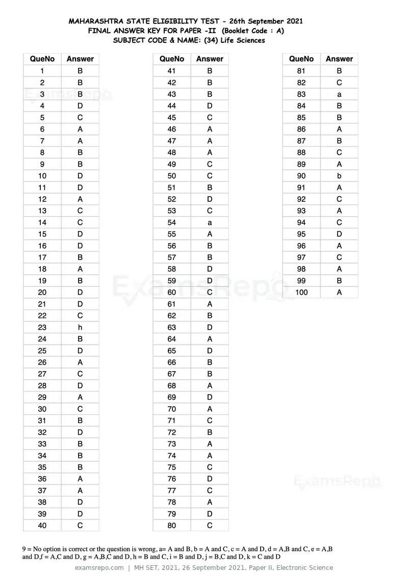
Text of page 81
MAHARASHTRA STATE ELIGIBILITY TEST - 26th September 2021
                    FINAL ANSWER KEY FOR PAPER -II (Booklet Code : A)
                          SUBJECT CODE & NAME: (34) Life Sciences

  QueNo        Answer                            QueNo        Answer                           QueNo        Answer
      1            B                               41             B                               81              B
      2            B                               42             B                               82              C
      3            B                               43             B                               83              a
      4            D                               44             D                               84              B
      5            C                               45             C                               85              B
      6            A                               46             A                               86              A
      7            A                               47             A                               87              B
      8            B                               48             A                               88              C
      9            B                               49             C                               89              A
     10            D                               50             C                               90              b
     11            D                               51             B                               91              A
     12            A                               52             D                               92              C
     13            C                               53             C                               93              A
     14            C                               54             a                               94              C
     15            D                               55             A                               95              D
     16            D                               56             B                               96              A
     17            B                               57             B                               97              C
     18            A                               58             D                               98              A
     19            B                               59             D                               99              B
     20            D                               60             C                              100              A
     21            D                               61             A
     22            C                               62             B
     23            h                               63             D
     24            B                               64             A
     25            D                               65             D
     26            A                               66             B
     27            C                               67             B
     28            D                               68             A
     29            A                               69             D
     30            C                               70             A
     31            B                               71             C
     32            D                               72             B
     33            B                               73             A
     34            B                               74             A
     35            B                               75             C
     36            A                               76             D
     37            A                               77             C
     38            D                               78             A
     39            D                               79             D
     40            C                               80             C


9 = No option is correct or the question is wrong, a= A and B, b = A and C, c = A and D, d = A,B and C, e = A,B
and D,f = A,C and D, g = A,B,C and D, h = B and C, i = B and D, j = B,C and D, k = C and D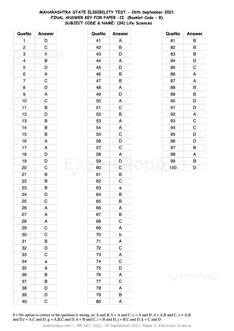
Text of page 82
MAHARASHTRA STATE ELIGIBILITY TEST - 26th September 2021
                    FINAL ANSWER KEY FOR PAPER -II (Booklet Code : B)
                          SUBJECT CODE & NAME: (34) Life Sciences

  QueNo        Answer                            QueNo        Answer                           QueNo        Answer
      1            D                               41             A                               81              B
      2            C                               42             B                               82              B
      3            h                               43             D                               83              B
      4            B                               44             A                               84              D
      5            D                               45             D                               85              C
      6            A                               46             B                               86              A
      7            C                               47             B                               87              A
      8            D                               48             A                               88              B
      9            A                               49             D                               89              B
     10            C                               50             A                               90              D
     11            B                               51             C                               91              D
     12            D                               52             B                               92              A
     13            B                               53             A                               93              C
     14            B                               54             A                               94              C
     15            B                               55             C                               95              D
     16            A                               56             D                               96              D
     17            A                               57             C                               97              B
     18            D                               58             A                               98              A
     19            D                               59             D                               99              B
     20            C                               60             C                              100              D
     21            B                               61             B
     22            B                               62             C
     23            B                               63             a
     24            D                               64             B
     25            C                               65             B
     26            A                               66             A
     27            A                               67             B
     28            A                               68             C
     29            C                               69             A
     30            C                               70             b
     31            B                               71             A
     32            D                               72             C
     33            C                               73             A
     34            a                               74             C
     35            A                               75             D
     36            B                               76             A
     37            B                               77             C
     38            D                               78             A
     39            D                               79             B
     40            C                               80             A


9 = No option is correct or the question is wrong, a= A and B, b = A and C, c = A and D, d = A,B and C, e = A,B
and D,f = A,C and D, g = A,B,C and D, h = B and C, i = B and D, j = B,C and D, k = C and D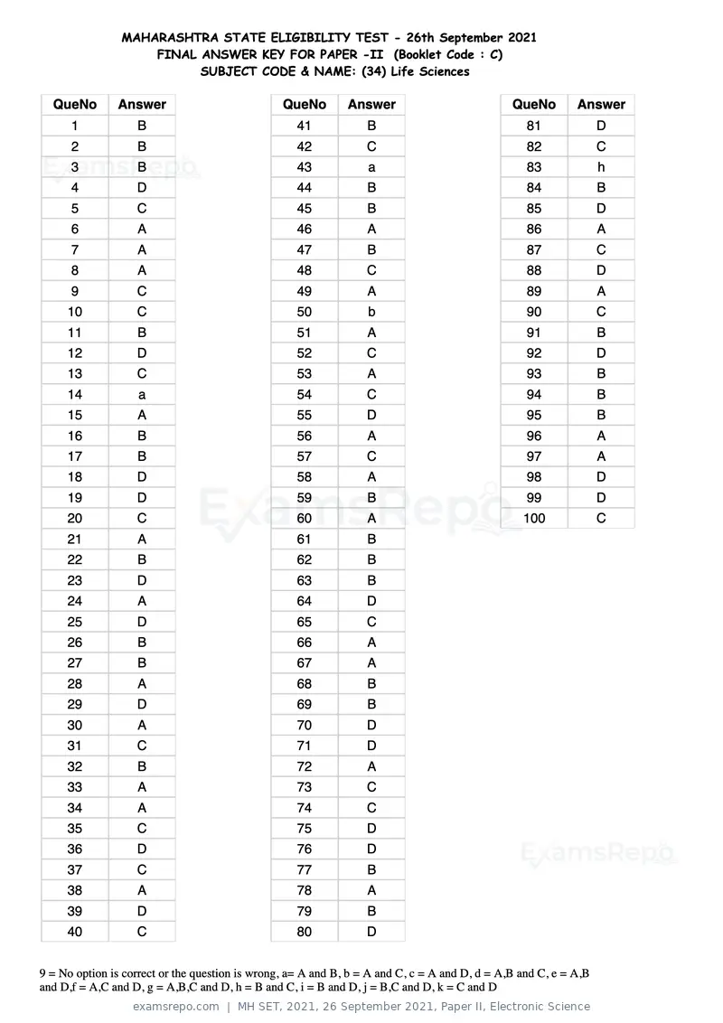
Text of page 83
MAHARASHTRA STATE ELIGIBILITY TEST - 26th September 2021
                    FINAL ANSWER KEY FOR PAPER -II (Booklet Code : C)
                          SUBJECT CODE & NAME: (34) Life Sciences

  QueNo        Answer                            QueNo        Answer                           QueNo        Answer
      1            B                               41             B                               81              D
      2            B                               42             C                               82              C
      3            B                               43             a                               83              h
      4            D                               44             B                               84              B
      5            C                               45             B                               85              D
      6            A                               46             A                               86              A
      7            A                               47             B                               87              C
      8            A                               48             C                               88              D
      9            C                               49             A                               89              A
     10            C                               50             b                               90              C
     11            B                               51             A                               91              B
     12            D                               52             C                               92              D
     13            C                               53             A                               93              B
     14            a                               54             C                               94              B
     15            A                               55             D                               95              B
     16            B                               56             A                               96              A
     17            B                               57             C                               97              A
     18            D                               58             A                               98              D
     19            D                               59             B                               99              D
     20            C                               60             A                              100              C
     21            A                               61             B
     22            B                               62             B
     23            D                               63             B
     24            A                               64             D
     25            D                               65             C
     26            B                               66             A
     27            B                               67             A
     28            A                               68             B
     29            D                               69             B
     30            A                               70             D
     31            C                               71             D
     32            B                               72             A
     33            A                               73             C
     34            A                               74             C
     35            C                               75             D
     36            D                               76             D
     37            C                               77             B
     38            A                               78             A
     39            D                               79             B
     40            C                               80             D


9 = No option is correct or the question is wrong, a= A and B, b = A and C, c = A and D, d = A,B and C, e = A,B
and D,f = A,C and D, g = A,B,C and D, h = B and C, i = B and D, j = B,C and D, k = C and D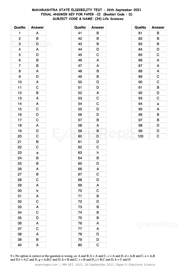
Text of page 84
MAHARASHTRA STATE ELIGIBILITY TEST - 26th September 2021
                    FINAL ANSWER KEY FOR PAPER -II (Booklet Code : D)
                          SUBJECT CODE & NAME: (34) Life Sciences

  QueNo        Answer                            QueNo        Answer                           QueNo        Answer
      1            A                               41             B                               81              B
      2            B                               42             B                               82              B
      3            D                               43             B                               83              B
      4            A                               44             D                               84              D
      5            D                               45             C                               85              C
      6            B                               46             A                               86              A
      7            B                               47             A                               87              A
      8            A                               48             B                               88              A
      9            D                               49             B                               89              C
     10            A                               50             D                               90              C
     11            C                               51             D                               91              B
     12            B                               52             A                               92              D
     13            A                               53             C                               93              C
     14            A                               54             C                               94              a
     15            C                               55             D                               95              A
     16            D                               56             D                               96              B
     17            C                               57             B                               97              B
     18            A                               58             A                               98              D
     19            D                               59             B                               99              D
     20            C                               60             D                              100              C
     21            B                               61             D
     22            C                               62             C
     23            a                               63             h
     24            B                               64             B
     25            B                               65             D
     26            A                               66             A
     27            B                               67             C
     28            C                               68             D
     29            A                               69             A
     30            b                               70             C
     31            A                               71             B
     32            C                               72             D
     33            A                               73             B
     34            C                               74             B
     35            D                               75             B
     36            A                               76             A
     37            C                               77             A
     38            A                               78             D
     39            B                               79             D
     40            A                               80             C


9 = No option is correct or the question is wrong, a= A and B, b = A and C, c = A and D, d = A,B and C, e = A,B
and D,f = A,C and D, g = A,B,C and D, h = B and C, i = B and D, j = B,C and D, k = C and D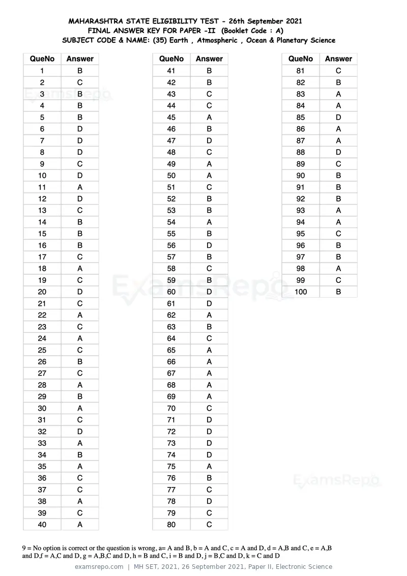
Text of page 85
MAHARASHTRA STATE ELIGIBILITY TEST - 26th September 2021
                    FINAL ANSWER KEY FOR PAPER -II (Booklet Code : A)
              SUBJECT CODE & NAME: (35) Earth , Atmospheric , Ocean & Planetary Science

  QueNo        Answer                            QueNo        Answer                           QueNo        Answer
      1            B                               41             B                               81              C
      2            C                               42             B                               82              B
      3            B                               43             C                               83              A
      4            B                               44             C                               84              A
      5            B                               45             A                               85              D
      6            D                               46             B                               86              A
      7            D                               47             D                               87              A
      8            D                               48             C                               88              D
      9            C                               49             A                               89              C
     10            D                               50             A                               90              B
     11            A                               51             C                               91              B
     12            D                               52             B                               92              B
     13            C                               53             B                               93              A
     14            B                               54             A                               94              A
     15            B                               55             B                               95              C
     16            B                               56             D                               96              B
     17            C                               57             B                               97              B
     18            A                               58             C                               98              A
     19            C                               59             B                               99              C
     20            D                               60             D                              100              B
     21            C                               61             D
     22            A                               62             A
     23            C                               63             B
     24            A                               64             C
     25            C                               65             A
     26            B                               66             A
     27            C                               67             A
     28            A                               68             A
     29            B                               69             A
     30            A                               70             C
     31            C                               71             D
     32            D                               72             D
     33            A                               73             D
     34            B                               74             D
     35            A                               75             A
     36            C                               76             B
     37            C                               77             C
     38            A                               78             D
     39            C                               79             C
     40            A                               80             C


9 = No option is correct or the question is wrong, a= A and B, b = A and C, c = A and D, d = A,B and C, e = A,B
and D,f = A,C and D, g = A,B,C and D, h = B and C, i = B and D, j = B,C and D, k = C and D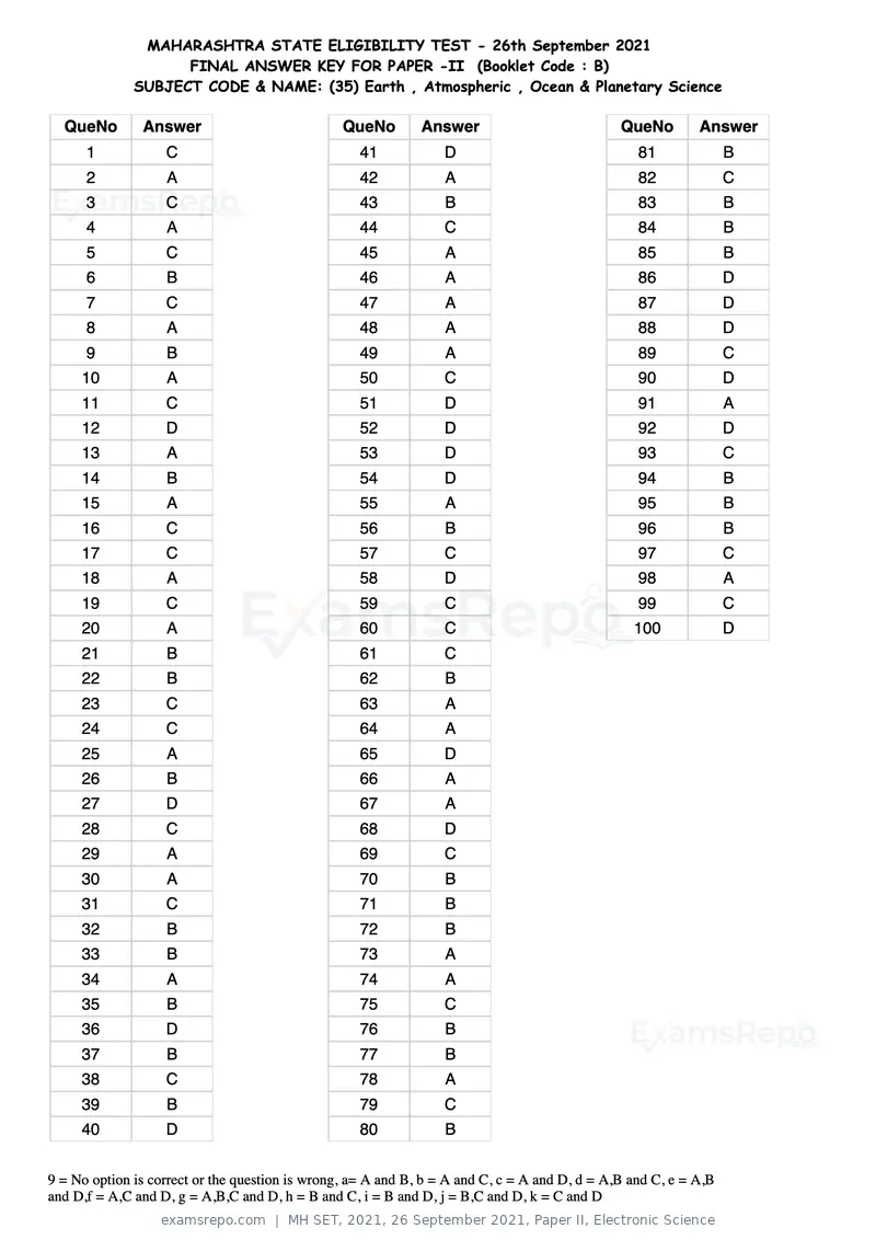
Text of page 86
MAHARASHTRA STATE ELIGIBILITY TEST - 26th September 2021
                    FINAL ANSWER KEY FOR PAPER -II (Booklet Code : B)
              SUBJECT CODE & NAME: (35) Earth , Atmospheric , Ocean & Planetary Science

  QueNo        Answer                            QueNo        Answer                           QueNo        Answer
      1            C                               41             D                               81              B
      2            A                               42             A                               82              C
      3            C                               43             B                               83              B
      4            A                               44             C                               84              B
      5            C                               45             A                               85              B
      6            B                               46             A                               86              D
      7            C                               47             A                               87              D
      8            A                               48             A                               88              D
      9            B                               49             A                               89              C
     10            A                               50             C                               90              D
     11            C                               51             D                               91              A
     12            D                               52             D                               92              D
     13            A                               53             D                               93              C
     14            B                               54             D                               94              B
     15            A                               55             A                               95              B
     16            C                               56             B                               96              B
     17            C                               57             C                               97              C
     18            A                               58             D                               98              A
     19            C                               59             C                               99              C
     20            A                               60             C                              100              D
     21            B                               61             C
     22            B                               62             B
     23            C                               63             A
     24            C                               64             A
     25            A                               65             D
     26            B                               66             A
     27            D                               67             A
     28            C                               68             D
     29            A                               69             C
     30            A                               70             B
     31            C                               71             B
     32            B                               72             B
     33            B                               73             A
     34            A                               74             A
     35            B                               75             C
     36            D                               76             B
     37            B                               77             B
     38            C                               78             A
     39            B                               79             C
     40            D                               80             B


9 = No option is correct or the question is wrong, a= A and B, b = A and C, c = A and D, d = A,B and C, e = A,B
and D,f = A,C and D, g = A,B,C and D, h = B and C, i = B and D, j = B,C and D, k = C and D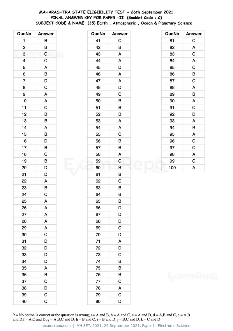
Text of page 87
MAHARASHTRA STATE ELIGIBILITY TEST - 26th September 2021
                    FINAL ANSWER KEY FOR PAPER -II (Booklet Code : C)
              SUBJECT CODE & NAME: (35) Earth , Atmospheric , Ocean & Planetary Science

  QueNo        Answer                            QueNo        Answer                           QueNo        Answer
      1            B                               41             C                               81              C
      2            B                               42             B                               82              A
      3            C                               43             A                               83              C
      4            C                               44             A                               84              A
      5            A                               45             D                               85              C
      6            B                               46             A                               86              B
      7            D                               47             A                               87              C
      8            C                               48             D                               88              A
      9            A                               49             C                               89              B
     10            A                               50             B                               90              A
     11            C                               51             B                               91              C
     12            B                               52             B                               92              D
     13            B                               53             A                               93              A
     14            A                               54             A                               94              B
     15            B                               55             C                               95              A
     16            D                               56             B                               96              C
     17            B                               57             B                               97              C
     18            C                               58             A                               98              A
     19            B                               59             C                               99              C
     20            D                               60             B                              100              A
     21            D                               61             B
     22            A                               62             C
     23            B                               63             B
     24            C                               64             B
     25            A                               65             B
     26            A                               66             D
     27            A                               67             D
     28            A                               68             D
     29            A                               69             C
     30            C                               70             D
     31            D                               71             A
     32            D                               72             D
     33            D                               73             C
     34            D                               74             B
     35            A                               75             B
     36            B                               76             B
     37            C                               77             C
     38            D                               78             A
     39            C                               79             C
     40            C                               80             D


9 = No option is correct or the question is wrong, a= A and B, b = A and C, c = A and D, d = A,B and C, e = A,B
and D,f = A,C and D, g = A,B,C and D, h = B and C, i = B and D, j = B,C and D, k = C and D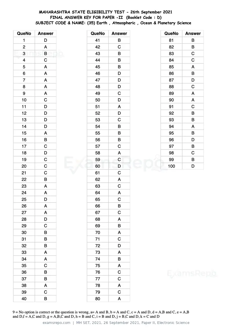
Text of page 88
MAHARASHTRA STATE ELIGIBILITY TEST - 26th September 2021
                    FINAL ANSWER KEY FOR PAPER -II (Booklet Code : D)
              SUBJECT CODE & NAME: (35) Earth , Atmospheric , Ocean & Planetary Science

  QueNo        Answer                            QueNo        Answer                           QueNo        Answer
      1            D                               41             B                               81              B
      2            A                               42             C                               82              B
      3            B                               43             B                               83              C
      4            C                               44             B                               84              C
      5            A                               45             B                               85              A
      6            A                               46             D                               86              B
      7            A                               47             D                               87              D
      8            A                               48             D                               88              C
      9            A                               49             C                               89              A
     10            C                               50             D                               90              A
     11            D                               51             A                               91              C
     12            D                               52             D                               92              B
     13            D                               53             C                               93              B
     14            D                               54             B                               94              A
     15            A                               55             B                               95              B
     16            B                               56             B                               96              D
     17            C                               57             C                               97              B
     18            D                               58             A                               98              C
     19            C                               59             C                               99              B
     20            C                               60             D                              100              D
     21            C                               61             C
     22            B                               62             A
     23            A                               63             C
     24            A                               64             A
     25            D                               65             C
     26            A                               66             B
     27            A                               67             C
     28            D                               68             A
     29            C                               69             B
     30            B                               70             A
     31            B                               71             C
     32            B                               72             D
     33            A                               73             A
     34            A                               74             B
     35            C                               75             A
     36            B                               76             C
     37            B                               77             C
     38            A                               78             A
     39            C                               79             C
     40            B                               80             A


9 = No option is correct or the question is wrong, a= A and B, b = A and C, c = A and D, d = A,B and C, e = A,B
and D,f = A,C and D, g = A,B,C and D, h = B and C, i = B and D, j = B,C and D, k = C and D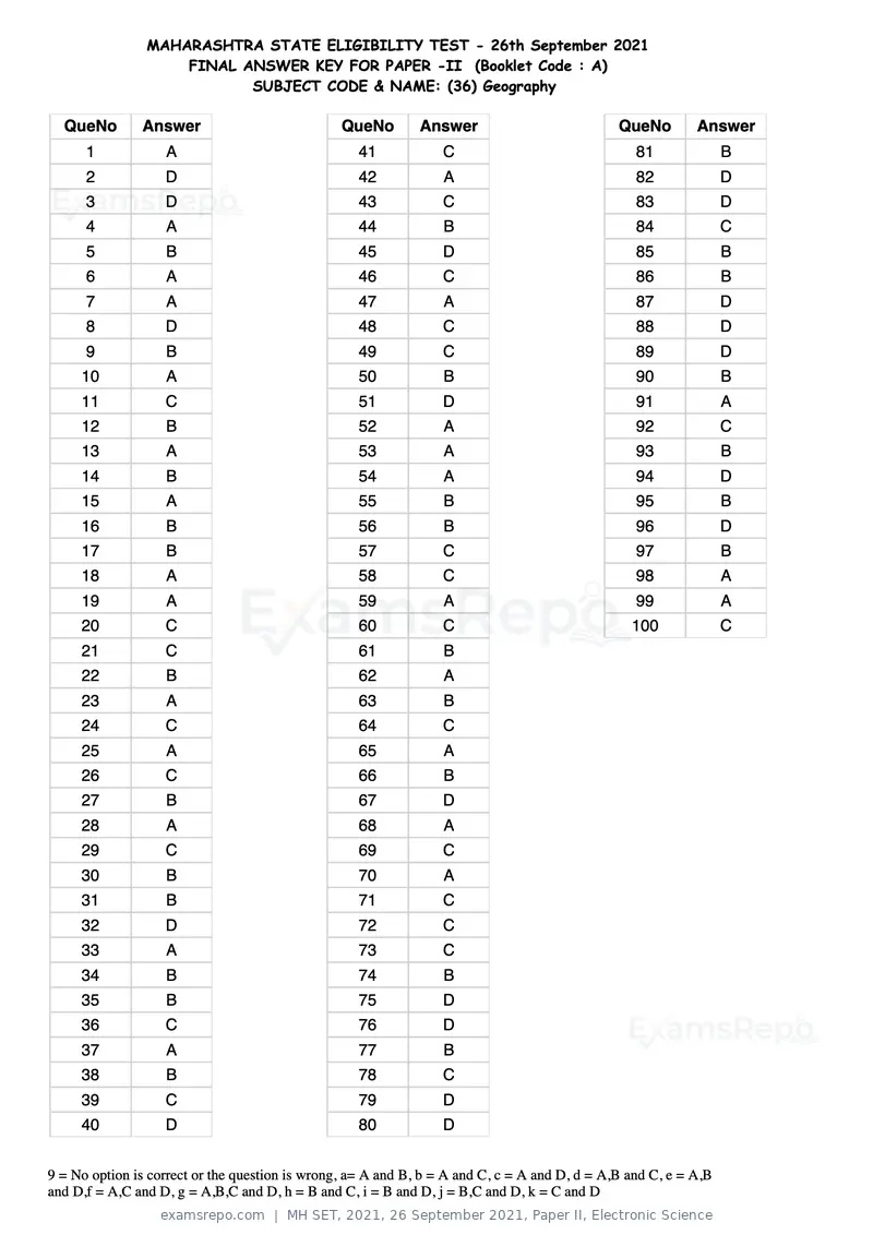
Text of page 89
MAHARASHTRA STATE ELIGIBILITY TEST - 26th September 2021
                    FINAL ANSWER KEY FOR PAPER -II (Booklet Code : A)
                           SUBJECT CODE & NAME: (36) Geography

  QueNo        Answer                            QueNo        Answer                           QueNo        Answer
      1            A                               41             C                               81              B
      2            D                               42             A                               82              D
      3            D                               43             C                               83              D
      4            A                               44             B                               84              C
      5            B                               45             D                               85              B
      6            A                               46             C                               86              B
      7            A                               47             A                               87              D
      8            D                               48             C                               88              D
      9            B                               49             C                               89              D
     10            A                               50             B                               90              B
     11            C                               51             D                               91              A
     12            B                               52             A                               92              C
     13            A                               53             A                               93              B
     14            B                               54             A                               94              D
     15            A                               55             B                               95              B
     16            B                               56             B                               96              D
     17            B                               57             C                               97              B
     18            A                               58             C                               98              A
     19            A                               59             A                               99              A
     20            C                               60             C                              100              C
     21            C                               61             B
     22            B                               62             A
     23            A                               63             B
     24            C                               64             C
     25            A                               65             A
     26            C                               66             B
     27            B                               67             D
     28            A                               68             A
     29            C                               69             C
     30            B                               70             A
     31            B                               71             C
     32            D                               72             C
     33            A                               73             C
     34            B                               74             B
     35            B                               75             D
     36            C                               76             D
     37            A                               77             B
     38            B                               78             C
     39            C                               79             D
     40            D                               80             D


9 = No option is correct or the question is wrong, a= A and B, b = A and C, c = A and D, d = A,B and C, e = A,B
and D,f = A,C and D, g = A,B,C and D, h = B and C, i = B and D, j = B,C and D, k = C and D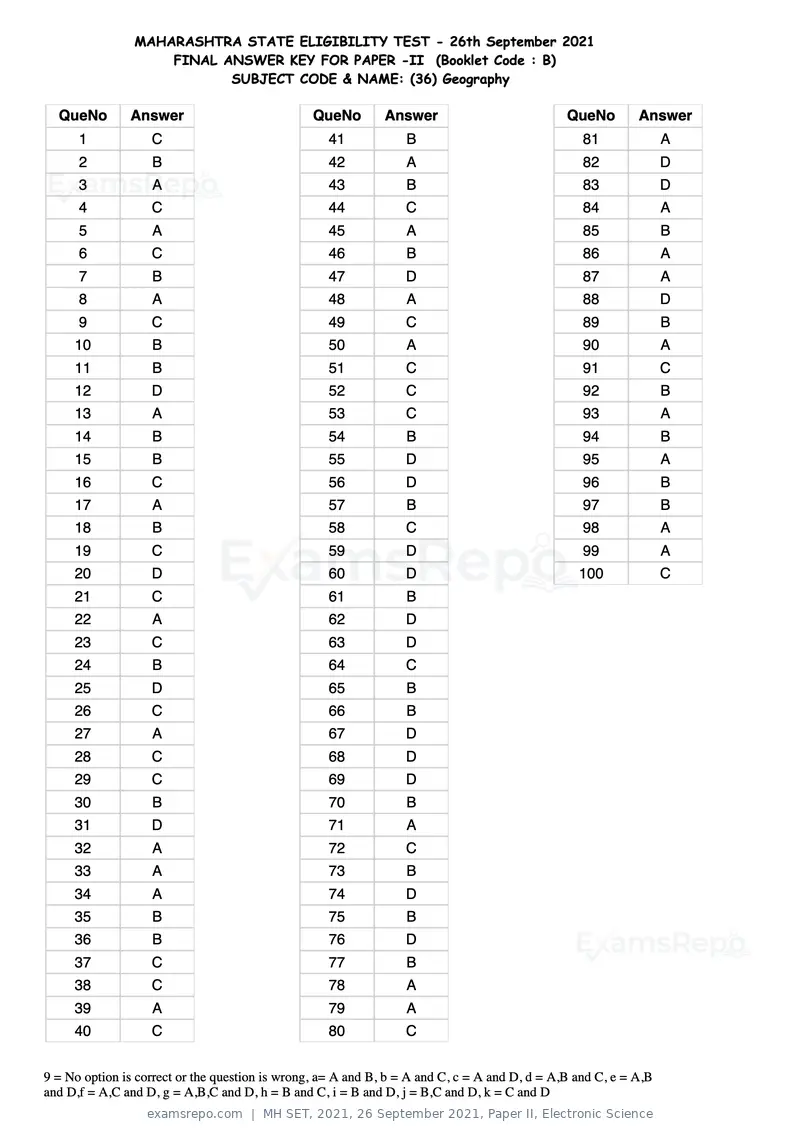
Text of page 90
MAHARASHTRA STATE ELIGIBILITY TEST - 26th September 2021
                    FINAL ANSWER KEY FOR PAPER -II (Booklet Code : B)
                           SUBJECT CODE & NAME: (36) Geography

  QueNo        Answer                            QueNo        Answer                           QueNo        Answer
      1            C                               41             B                               81              A
      2            B                               42             A                               82              D
      3            A                               43             B                               83              D
      4            C                               44             C                               84              A
      5            A                               45             A                               85              B
      6            C                               46             B                               86              A
      7            B                               47             D                               87              A
      8            A                               48             A                               88              D
      9            C                               49             C                               89              B
     10            B                               50             A                               90              A
     11            B                               51             C                               91              C
     12            D                               52             C                               92              B
     13            A                               53             C                               93              A
     14            B                               54             B                               94              B
     15            B                               55             D                               95              A
     16            C                               56             D                               96              B
     17            A                               57             B                               97              B
     18            B                               58             C                               98              A
     19            C                               59             D                               99              A
     20            D                               60             D                              100              C
     21            C                               61             B
     22            A                               62             D
     23            C                               63             D
     24            B                               64             C
     25            D                               65             B
     26            C                               66             B
     27            A                               67             D
     28            C                               68             D
     29            C                               69             D
     30            B                               70             B
     31            D                               71             A
     32            A                               72             C
     33            A                               73             B
     34            A                               74             D
     35            B                               75             B
     36            B                               76             D
     37            C                               77             B
     38            C                               78             A
     39            A                               79             A
     40            C                               80             C


9 = No option is correct or the question is wrong, a= A and B, b = A and C, c = A and D, d = A,B and C, e = A,B
and D,f = A,C and D, g = A,B,C and D, h = B and C, i = B and D, j = B,C and D, k = C and D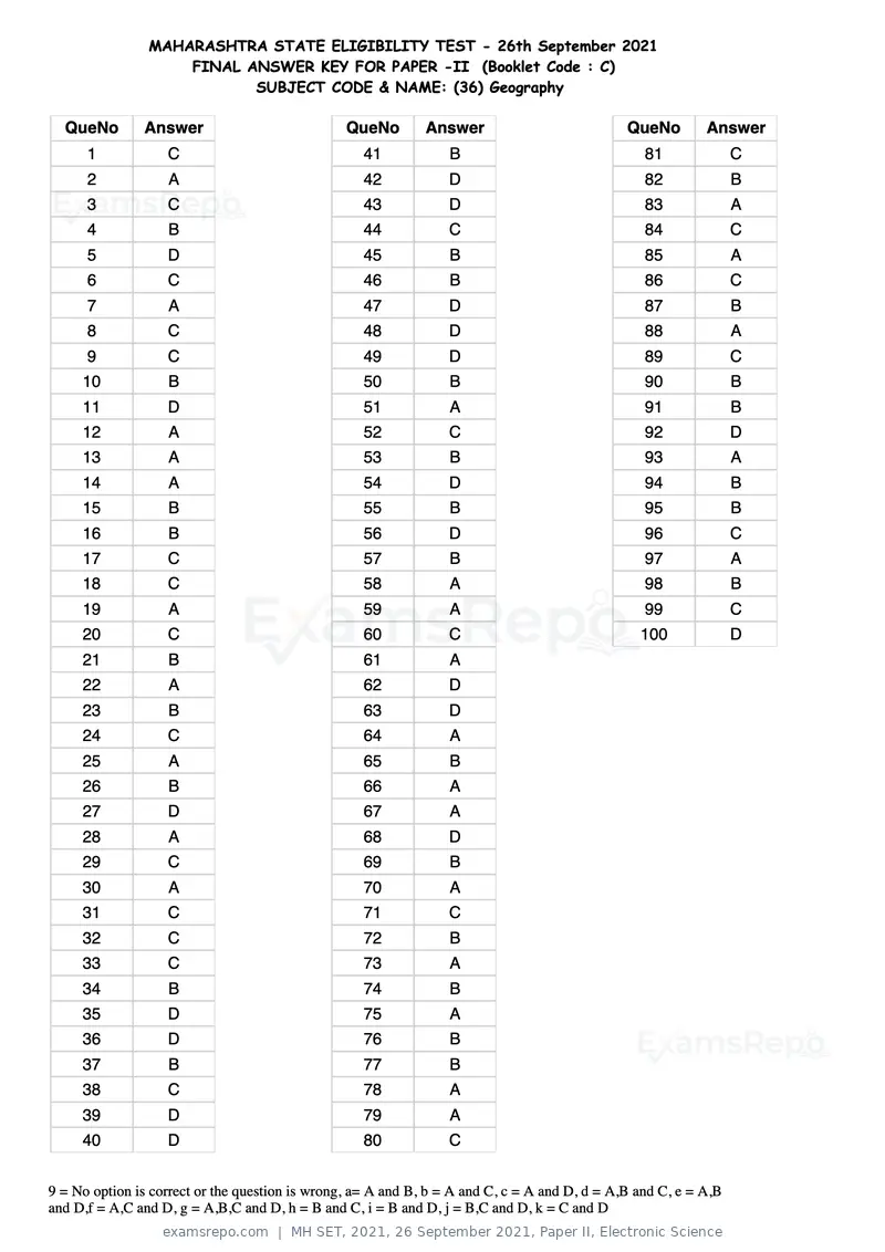
Text of page 91
MAHARASHTRA STATE ELIGIBILITY TEST - 26th September 2021
                    FINAL ANSWER KEY FOR PAPER -II (Booklet Code : C)
                           SUBJECT CODE & NAME: (36) Geography

  QueNo        Answer                            QueNo        Answer                           QueNo        Answer
      1            C                               41             B                               81              C
      2            A                               42             D                               82              B
      3            C                               43             D                               83              A
      4            B                               44             C                               84              C
      5            D                               45             B                               85              A
      6            C                               46             B                               86              C
      7            A                               47             D                               87              B
      8            C                               48             D                               88              A
      9            C                               49             D                               89              C
     10            B                               50             B                               90              B
     11            D                               51             A                               91              B
     12            A                               52             C                               92              D
     13            A                               53             B                               93              A
     14            A                               54             D                               94              B
     15            B                               55             B                               95              B
     16            B                               56             D                               96              C
     17            C                               57             B                               97              A
     18            C                               58             A                               98              B
     19            A                               59             A                               99              C
     20            C                               60             C                              100              D
     21            B                               61             A
     22            A                               62             D
     23            B                               63             D
     24            C                               64             A
     25            A                               65             B
     26            B                               66             A
     27            D                               67             A
     28            A                               68             D
     29            C                               69             B
     30            A                               70             A
     31            C                               71             C
     32            C                               72             B
     33            C                               73             A
     34            B                               74             B
     35            D                               75             A
     36            D                               76             B
     37            B                               77             B
     38            C                               78             A
     39            D                               79             A
     40            D                               80             C


9 = No option is correct or the question is wrong, a= A and B, b = A and C, c = A and D, d = A,B and C, e = A,B
and D,f = A,C and D, g = A,B,C and D, h = B and C, i = B and D, j = B,C and D, k = C and D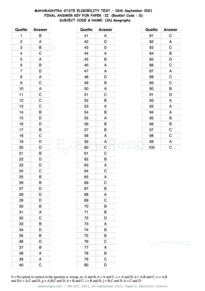
Text of page 92
MAHARASHTRA STATE ELIGIBILITY TEST - 26th September 2021
                    FINAL ANSWER KEY FOR PAPER -II (Booklet Code : D)
                           SUBJECT CODE & NAME: (36) Geography

  QueNo        Answer                            QueNo        Answer                           QueNo        Answer
      1            B                               41             A                               81              C
      2            A                               42             D                               82              A
      3            B                               43             D                               83              C
      4            C                               44             A                               84              B
      5            A                               45             B                               85              D
      6            B                               46             A                               86              C
      7            D                               47             A                               87              A
      8            A                               48             D                               88              C
      9            C                               49             B                               89              C
     10            A                               50             A                               90              B
     11            C                               51             C                               91              D
     12            C                               52             B                               92              A
     13            C                               53             A                               93              A
     14            B                               54             B                               94              A
     15            D                               55             A                               95              B
     16            D                               56             B                               96              B
     17            B                               57             B                               97              C
     18            C                               58             A                               98              C
     19            D                               59             A                               99              A
     20            D                               60             C                              100              C
     21            B                               61             C
     22            D                               62             B
     23            D                               63             A
     24            C                               64             C
     25            B                               65             A
     26            B                               66             C
     27            D                               67             B
     28            D                               68             A
     29            D                               69             C
     30            B                               70             B
     31            A                               71             B
     32            C                               72             D
     33            B                               73             A
     34            D                               74             B
     35            B                               75             B
     36            D                               76             C
     37            B                               77             A
     38            A                               78             B
     39            A                               79             C
     40            C                               80             D


9 = No option is correct or the question is wrong, a= A and B, b = A and C, c = A and D, d = A,B and C, e = A,B
and D,f = A,C and D, g = A,B,C and D, h = B and C, i = B and D, j = B,C and D, k = C and D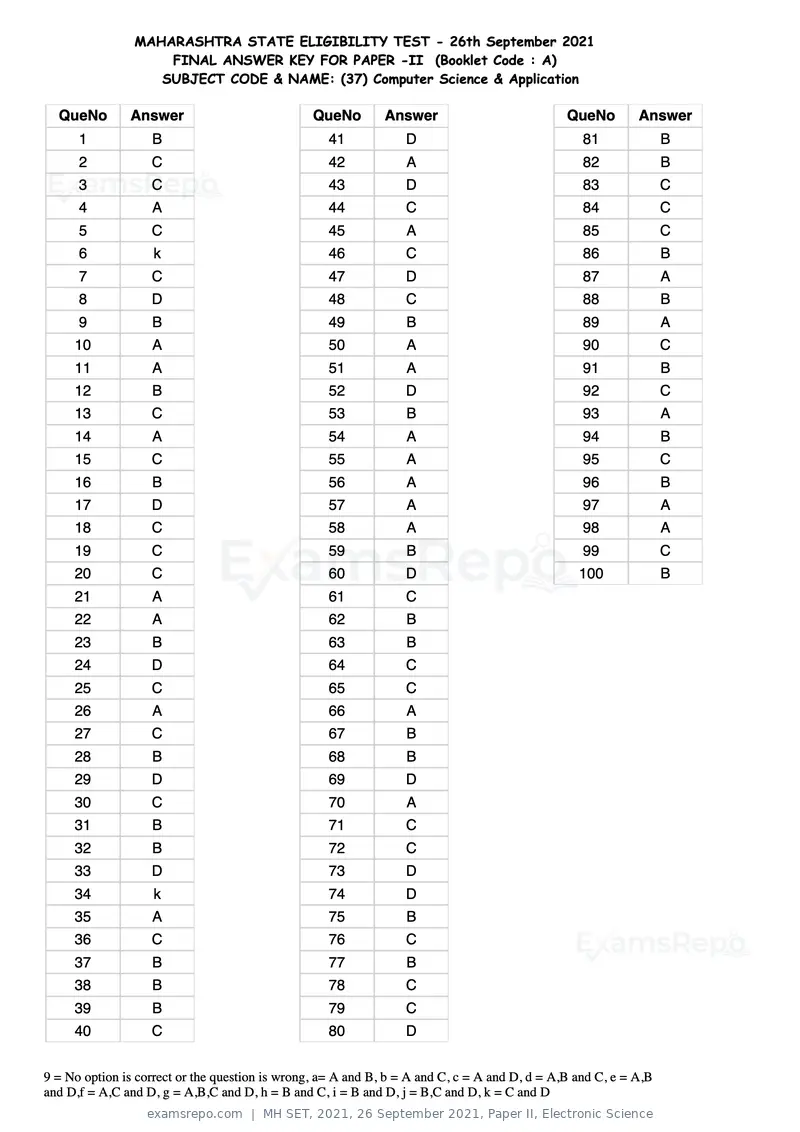
Text of page 93
MAHARASHTRA STATE ELIGIBILITY TEST - 26th September 2021
                    FINAL ANSWER KEY FOR PAPER -II (Booklet Code : A)
                   SUBJECT CODE & NAME: (37) Computer Science & Application

  QueNo        Answer                            QueNo        Answer                           QueNo        Answer
      1            B                               41             D                               81              B
      2            C                               42             A                               82              B
      3            C                               43             D                               83              C
      4            A                               44             C                               84              C
      5            C                               45             A                               85              C
      6             k                              46             C                               86              B
      7            C                               47             D                               87              A
      8            D                               48             C                               88              B
      9            B                               49             B                               89              A
     10            A                               50             A                               90              C
     11            A                               51             A                               91              B
     12            B                               52             D                               92              C
     13            C                               53             B                               93              A
     14            A                               54             A                               94              B
     15            C                               55             A                               95              C
     16            B                               56             A                               96              B
     17            D                               57             A                               97              A
     18            C                               58             A                               98              A
     19            C                               59             B                               99              C
     20            C                               60             D                              100              B
     21            A                               61             C
     22            A                               62             B
     23            B                               63             B
     24            D                               64             C
     25            C                               65             C
     26            A                               66             A
     27            C                               67             B
     28            B                               68             B
     29            D                               69             D
     30            C                               70             A
     31            B                               71             C
     32            B                               72             C
     33            D                               73             D
     34             k                              74             D
     35            A                               75             B
     36            C                               76             C
     37            B                               77             B
     38            B                               78             C
     39            B                               79             C
     40            C                               80             D


9 = No option is correct or the question is wrong, a= A and B, b = A and C, c = A and D, d = A,B and C, e = A,B
and D,f = A,C and D, g = A,B,C and D, h = B and C, i = B and D, j = B,C and D, k = C and D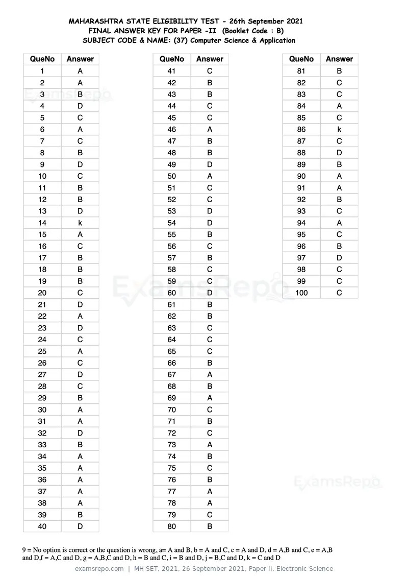
Text of page 94
MAHARASHTRA STATE ELIGIBILITY TEST - 26th September 2021
                    FINAL ANSWER KEY FOR PAPER -II (Booklet Code : B)
                   SUBJECT CODE & NAME: (37) Computer Science & Application

  QueNo        Answer                            QueNo        Answer                           QueNo        Answer
      1            A                               41             C                               81              B
      2            A                               42             B                               82              C
      3            B                               43             B                               83              C
      4            D                               44             C                               84              A
      5            C                               45             C                               85              C
      6            A                               46             A                               86              k
      7            C                               47             B                               87              C
      8            B                               48             B                               88              D
      9            D                               49             D                               89              B
     10            C                               50             A                               90              A
     11            B                               51             C                               91              A
     12            B                               52             C                               92              B
     13            D                               53             D                               93              C
     14             k                              54             D                               94              A
     15            A                               55             B                               95              C
     16            C                               56             C                               96              B
     17            B                               57             B                               97              D
     18            B                               58             C                               98              C
     19            B                               59             C                               99              C
     20            C                               60             D                              100              C
     21            D                               61             B
     22            A                               62             B
     23            D                               63             C
     24            C                               64             C
     25            A                               65             C
     26            C                               66             B
     27            D                               67             A
     28            C                               68             B
     29            B                               69             A
     30            A                               70             C
     31            A                               71             B
     32            D                               72             C
     33            B                               73             A
     34            A                               74             B
     35            A                               75             C
     36            A                               76             B
     37            A                               77             A
     38            A                               78             A
     39            B                               79             C
     40            D                               80             B


9 = No option is correct or the question is wrong, a= A and B, b = A and C, c = A and D, d = A,B and C, e = A,B
and D,f = A,C and D, g = A,B,C and D, h = B and C, i = B and D, j = B,C and D, k = C and D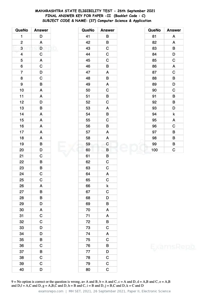
Text of page 95
MAHARASHTRA STATE ELIGIBILITY TEST - 26th September 2021
                    FINAL ANSWER KEY FOR PAPER -II (Booklet Code : C)
                   SUBJECT CODE & NAME: (37) Computer Science & Application

  QueNo        Answer                            QueNo        Answer                           QueNo        Answer
      1            D                               41             B                               81              A
      2            A                               42             B                               82              A
      3            D                               43             C                               83              B
      4            C                               44             C                               84              D
      5            A                               45             C                               85              C
      6            C                               46             B                               86              A
      7            D                               47             A                               87              C
      8            C                               48             B                               88              B
      9            B                               49             A                               89              D
     10            A                               50             C                               90              C
     11            A                               51             B                               91              B
     12            D                               52             C                               92              B
     13            B                               53             A                               93              D
     14            A                               54             B                               94              k
     15            A                               55             C                               95              A
     16            A                               56             B                               96              C
     17            A                               57             A                               97              B
     18            A                               58             A                               98              B
     19            B                               59             C                               99              B
     20            D                               60             B                              100              C
     21            C                               61             B
     22            B                               62             C
     23            B                               63             C
     24            C                               64             A
     25            C                               65             C
     26            A                               66             k
     27            B                               67             C
     28            B                               68             D
     29            D                               69             B
     30            A                               70             A
     31            C                               71             A
     32            C                               72             B
     33            D                               73             C
     34            D                               74             A
     35            B                               75             C
     36            C                               76             B
     37            B                               77             D
     38            C                               78             C
     39            C                               79             C
     40            D                               80             C


9 = No option is correct or the question is wrong, a= A and B, b = A and C, c = A and D, d = A,B and C, e = A,B
and D,f = A,C and D, g = A,B,C and D, h = B and C, i = B and D, j = B,C and D, k = C and D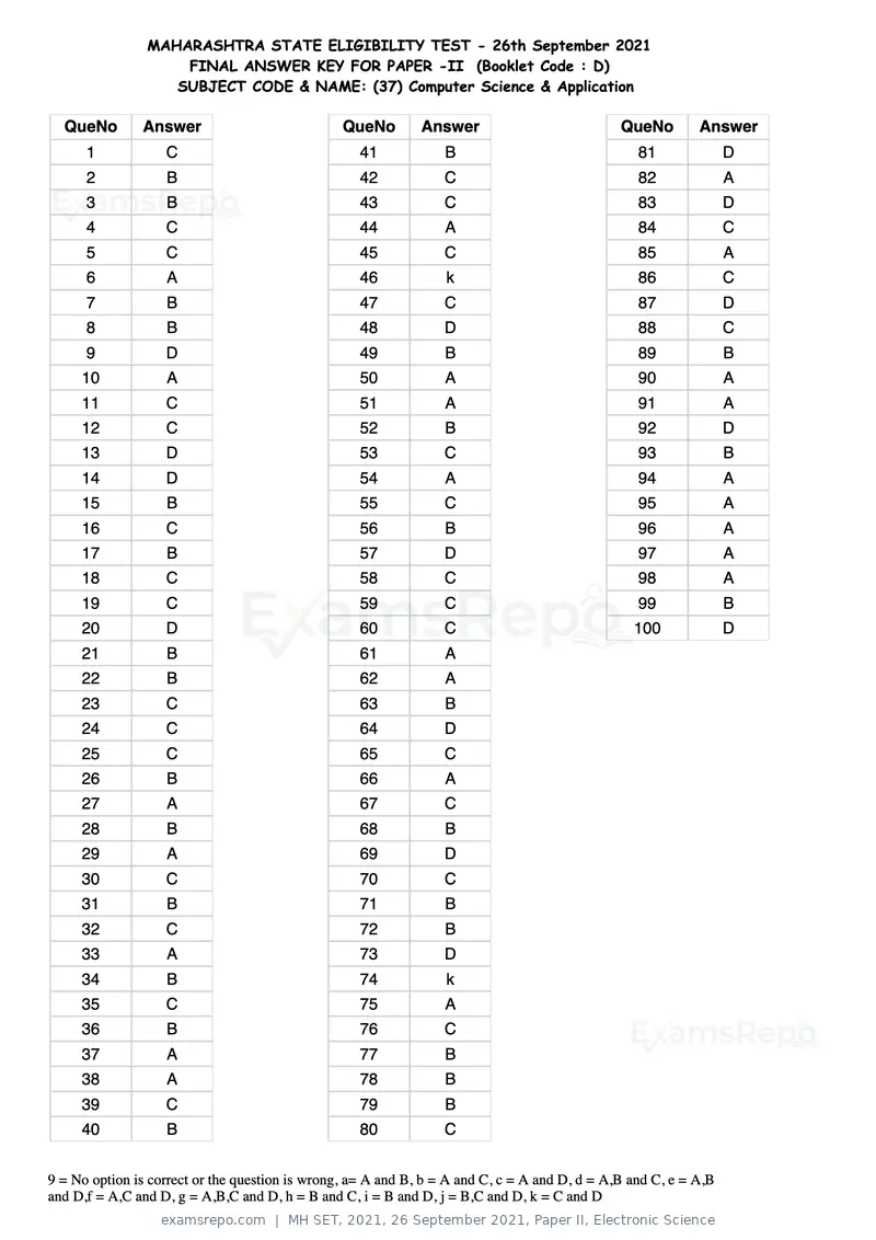
Text of page 96
MAHARASHTRA STATE ELIGIBILITY TEST - 26th September 2021
                    FINAL ANSWER KEY FOR PAPER -II (Booklet Code : D)
                   SUBJECT CODE & NAME: (37) Computer Science & Application

  QueNo        Answer                            QueNo        Answer                           QueNo        Answer
      1            C                               41             B                               81              D
      2            B                               42             C                               82              A
      3            B                               43             C                               83              D
      4            C                               44             A                               84              C
      5            C                               45             C                               85              A
      6            A                               46             k                               86              C
      7            B                               47             C                               87              D
      8            B                               48             D                               88              C
      9            D                               49             B                               89              B
     10            A                               50             A                               90              A
     11            C                               51             A                               91              A
     12            C                               52             B                               92              D
     13            D                               53             C                               93              B
     14            D                               54             A                               94              A
     15            B                               55             C                               95              A
     16            C                               56             B                               96              A
     17            B                               57             D                               97              A
     18            C                               58             C                               98              A
     19            C                               59             C                               99              B
     20            D                               60             C                              100              D
     21            B                               61             A
     22            B                               62             A
     23            C                               63             B
     24            C                               64             D
     25            C                               65             C
     26            B                               66             A
     27            A                               67             C
     28            B                               68             B
     29            A                               69             D
     30            C                               70             C
     31            B                               71             B
     32            C                               72             B
     33            A                               73             D
     34            B                               74             k
     35            C                               75             A
     36            B                               76             C
     37            A                               77             B
     38            A                               78             B
     39            C                               79             B
     40            B                               80             C


9 = No option is correct or the question is wrong, a= A and B, b = A and C, c = A and D, d = A,B and C, e = A,B
and D,f = A,C and D, g = A,B,C and D, h = B and C, i = B and D, j = B,C and D, k = C and D
Text of page 97
MAHARASHTRA STATE ELIGIBILITY TEST - 26th September 2021
                    FINAL ANSWER KEY FOR PAPER -II (Booklet Code : A)
                       SUBJECT CODE & NAME: (38) Electronics Science

  QueNo        Answer                            QueNo        Answer                           QueNo        Answer
      1            A                               41             A                               81              B
      2            C                               42             D                               82              B
      3            D                               43             B                               83              C
      4            B                               44             B                               84              B
      5            A                               45             C                               85              B
      6            B                               46             C                               86              A
      7            A                               47             C                               87              D
      8            D                               48             C                               88              C
      9            B                               49             B                               89              B
     10            D                               50             B                               90              a
     11            D                               51             C                               91              B
     12            C                               52             C                               92              C
     13            B                               53             B                               93              A
     14            B                               54             D                               94              D
     15            B                               55             D                               95              C
     16            D                               56             C                               96              A
     17            A                               57             A                               97              B
     18            C                               58             C                               98              D
     19            A                               59             B                               99              B
     20            A                               60             9                              100              B
     21            D                               61             D
     22            B                               62             A
     23            A                               63             C
     24            C                               64             B
     25            D                               65             A
     26            B                               66             C
     27            B                               67             B
     28            C                               68             C
     29            B                               69             A
     30            A                               70             D
     31            B                               71             D
     32            B                               72             D
     33            D                               73             B
     34            D                               74             B
     35            A                               75             C
     36            D                               76             B
     37            C                               77             B
     38            C                               78             A
     39            C                               79             D
     40            A                               80             B


9 = No option is correct or the question is wrong, a= A and B, b = A and C, c = A and D, d = A,B and C, e = A,B
and D,f = A,C and D, g = A,B,C and D, h = B and C, i = B and D, j = B,C and D, k = C and D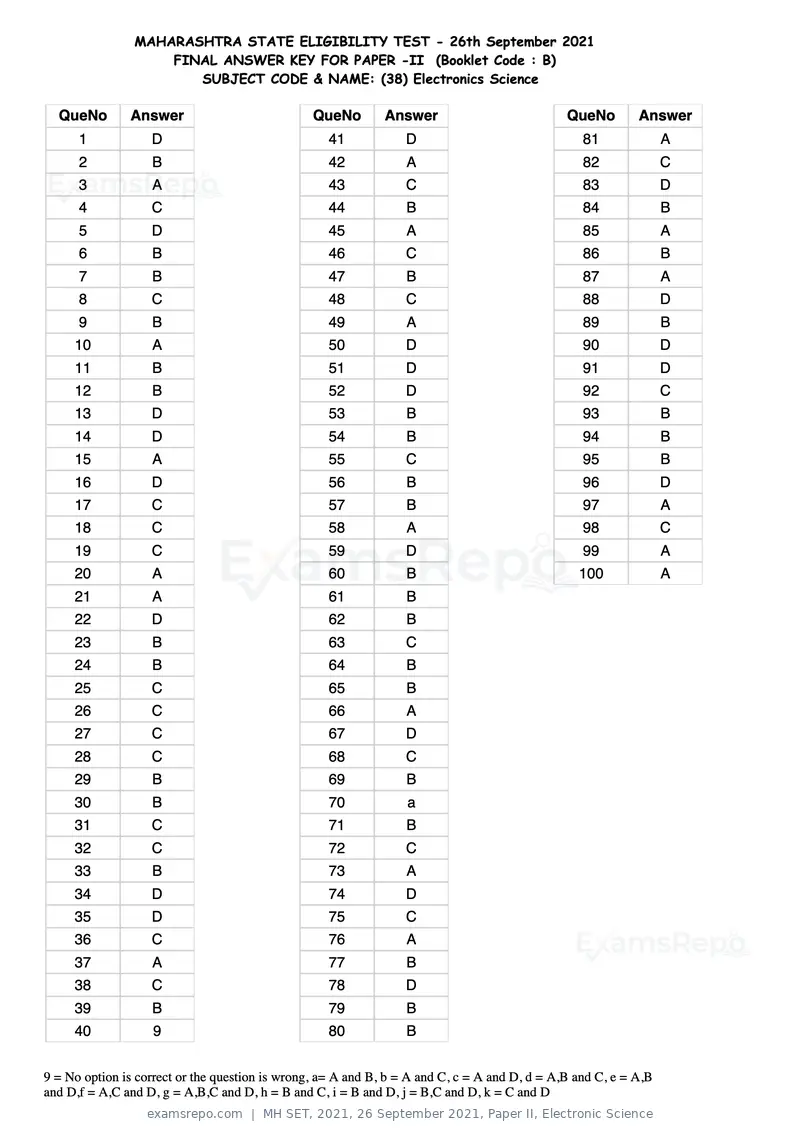
Text of page 98
MAHARASHTRA STATE ELIGIBILITY TEST - 26th September 2021
                    FINAL ANSWER KEY FOR PAPER -II (Booklet Code : B)
                       SUBJECT CODE & NAME: (38) Electronics Science

  QueNo        Answer                            QueNo        Answer                           QueNo        Answer
      1            D                               41             D                               81              A
      2            B                               42             A                               82              C
      3            A                               43             C                               83              D
      4            C                               44             B                               84              B
      5            D                               45             A                               85              A
      6            B                               46             C                               86              B
      7            B                               47             B                               87              A
      8            C                               48             C                               88              D
      9            B                               49             A                               89              B
     10            A                               50             D                               90              D
     11            B                               51             D                               91              D
     12            B                               52             D                               92              C
     13            D                               53             B                               93              B
     14            D                               54             B                               94              B
     15            A                               55             C                               95              B
     16            D                               56             B                               96              D
     17            C                               57             B                               97              A
     18            C                               58             A                               98              C
     19            C                               59             D                               99              A
     20            A                               60             B                              100              A
     21            A                               61             B
     22            D                               62             B
     23            B                               63             C
     24            B                               64             B
     25            C                               65             B
     26            C                               66             A
     27            C                               67             D
     28            C                               68             C
     29            B                               69             B
     30            B                               70             a
     31            C                               71             B
     32            C                               72             C
     33            B                               73             A
     34            D                               74             D
     35            D                               75             C
     36            C                               76             A
     37            A                               77             B
     38            C                               78             D
     39            B                               79             B
     40            9                               80             B


9 = No option is correct or the question is wrong, a= A and B, b = A and C, c = A and D, d = A,B and C, e = A,B
and D,f = A,C and D, g = A,B,C and D, h = B and C, i = B and D, j = B,C and D, k = C and D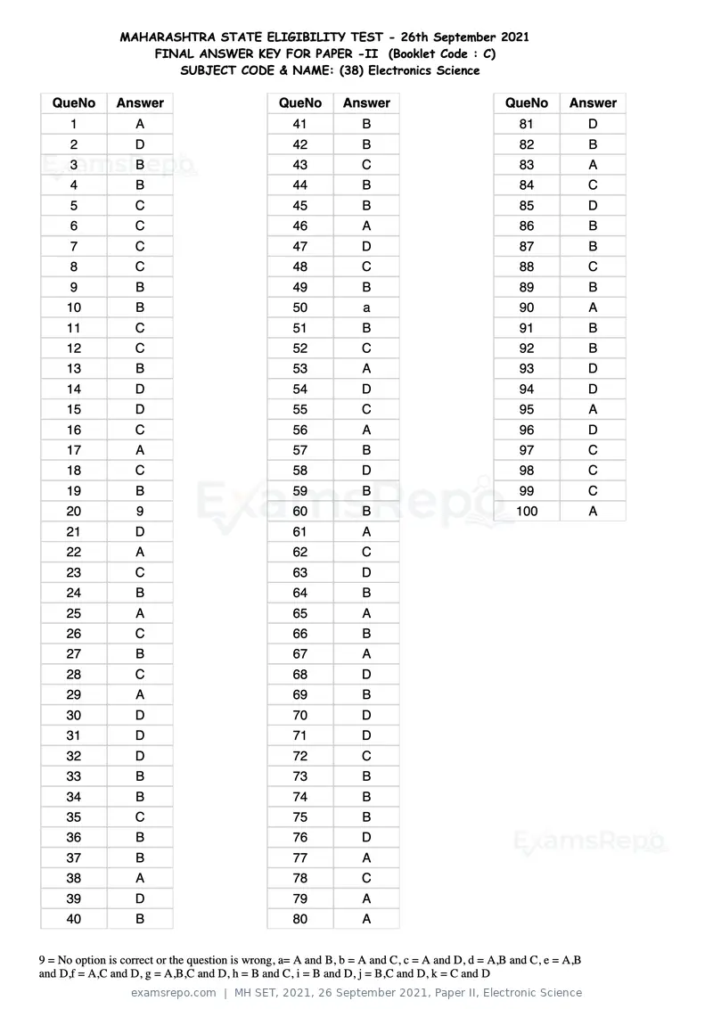
Text of page 99
MAHARASHTRA STATE ELIGIBILITY TEST - 26th September 2021
                    FINAL ANSWER KEY FOR PAPER -II (Booklet Code : C)
                       SUBJECT CODE & NAME: (38) Electronics Science

  QueNo        Answer                            QueNo        Answer                           QueNo        Answer
      1            A                               41             B                               81              D
      2            D                               42             B                               82              B
      3            B                               43             C                               83              A
      4            B                               44             B                               84              C
      5            C                               45             B                               85              D
      6            C                               46             A                               86              B
      7            C                               47             D                               87              B
      8            C                               48             C                               88              C
      9            B                               49             B                               89              B
     10            B                               50             a                               90              A
     11            C                               51             B                               91              B
     12            C                               52             C                               92              B
     13            B                               53             A                               93              D
     14            D                               54             D                               94              D
     15            D                               55             C                               95              A
     16            C                               56             A                               96              D
     17            A                               57             B                               97              C
     18            C                               58             D                               98              C
     19            B                               59             B                               99              C
     20            9                               60             B                              100              A
     21            D                               61             A
     22            A                               62             C
     23            C                               63             D
     24            B                               64             B
     25            A                               65             A
     26            C                               66             B
     27            B                               67             A
     28            C                               68             D
     29            A                               69             B
     30            D                               70             D
     31            D                               71             D
     32            D                               72             C
     33            B                               73             B
     34            B                               74             B
     35            C                               75             B
     36            B                               76             D
     37            B                               77             A
     38            A                               78             C
     39            D                               79             A
     40            B                               80             A


9 = No option is correct or the question is wrong, a= A and B, b = A and C, c = A and D, d = A,B and C, e = A,B
and D,f = A,C and D, g = A,B,C and D, h = B and C, i = B and D, j = B,C and D, k = C and D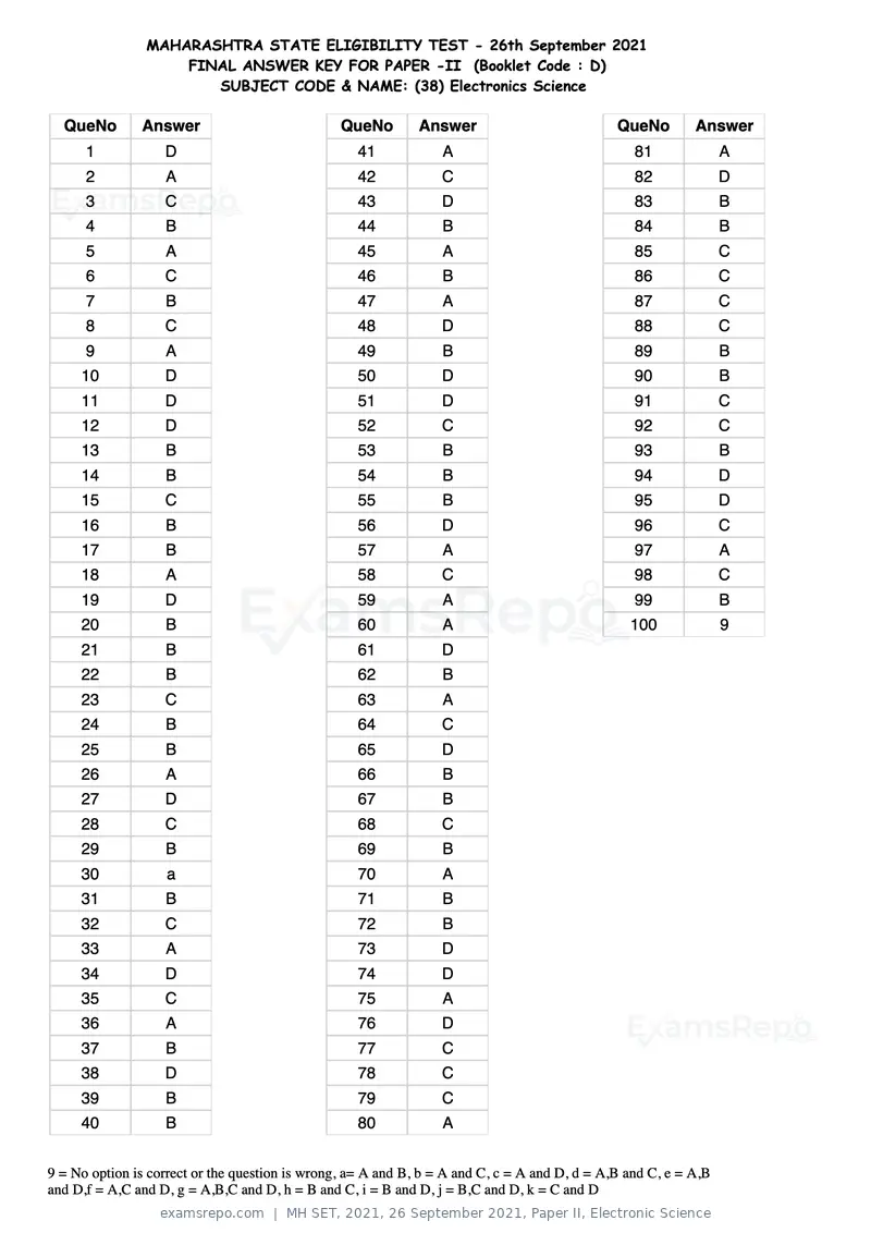
Text of page 100
MAHARASHTRA STATE ELIGIBILITY TEST - 26th September 2021
                    FINAL ANSWER KEY FOR PAPER -II (Booklet Code : D)
                       SUBJECT CODE & NAME: (38) Electronics Science

  QueNo        Answer                            QueNo        Answer                           QueNo        Answer
      1            D                               41             A                               81              A
      2            A                               42             C                               82              D
      3            C                               43             D                               83              B
      4            B                               44             B                               84              B
      5            A                               45             A                               85              C
      6            C                               46             B                               86              C
      7            B                               47             A                               87              C
      8            C                               48             D                               88              C
      9            A                               49             B                               89              B
     10            D                               50             D                               90              B
     11            D                               51             D                               91              C
     12            D                               52             C                               92              C
     13            B                               53             B                               93              B
     14            B                               54             B                               94              D
     15            C                               55             B                               95              D
     16            B                               56             D                               96              C
     17            B                               57             A                               97              A
     18            A                               58             C                               98              C
     19            D                               59             A                               99              B
     20            B                               60             A                              100              9
     21            B                               61             D
     22            B                               62             B
     23            C                               63             A
     24            B                               64             C
     25            B                               65             D
     26            A                               66             B
     27            D                               67             B
     28            C                               68             C
     29            B                               69             B
     30            a                               70             A
     31            B                               71             B
     32            C                               72             B
     33            A                               73             D
     34            D                               74             D
     35            C                               75             A
     36            A                               76             D
     37            B                               77             C
     38            D                               78             C
     39            B                               79             C
     40            B                               80             A


9 = No option is correct or the question is wrong, a= A and B, b = A and C, c = A and D, d = A,B and C, e = A,B
and D,f = A,C and D, g = A,B,C and D, h = B and C, i = B and D, j = B,C and D, k = C and D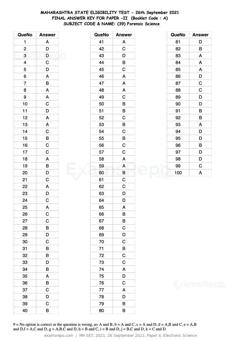
Text of page 101
MAHARASHTRA STATE ELIGIBILITY TEST - 26th September 2021
                    FINAL ANSWER KEY FOR PAPER -II (Booklet Code : A)
                        SUBJECT CODE & NAME: (39) Forensic Science

  QueNo        Answer                            QueNo        Answer                           QueNo        Answer
      1            A                               41             A                               81              D
      2            D                               42             C                               82              B
      3            D                               43             D                               83              A
      4            C                               44             B                               84              A
      5            D                               45             C                               85              A
      6            A                               46             A                               86              D
      7            B                               47             A                               87              C
      8            A                               48             A                               88              C
      9            A                               49             C                               89              D
     10            C                               50             B                               90              D
     11            D                               51             B                               91              B
     12            A                               52             C                               92              B
     13            A                               53             B                               93              A
     14            C                               54             C                               94              D
     15            B                               55             B                               95              D
     16            C                               56             C                               96              B
     17            C                               57             C                               97              D
     18            A                               58             A                               98              D
     19            B                               59             A                               99              C
     20            D                               60             B                              100              A
     21            C                               61             C
     22            A                               62             C
     23            D                               63             D
     24            C                               64             D
     25            A                               65             A
     26            C                               66             B
     27            C                               67             B
     28            B                               68             C
     29            D                               69             D
     30            C                               70             C
     31            B                               71             B
     32            B                               72             C
     33            D                               73             C
     34            B                               74             A
     35            A                               75             D
     36            B                               76             C
     37            C                               77             A
     38            D                               78             D
     39            C                               79             B
     40            B                               80             B


9 = No option is correct or the question is wrong, a= A and B, b = A and C, c = A and D, d = A,B and C, e = A,B
and D,f = A,C and D, g = A,B,C and D, h = B and C, i = B and D, j = B,C and D, k = C and D
Text of page 102
MAHARASHTRA STATE ELIGIBILITY TEST - 26th September 2021
                    FINAL ANSWER KEY FOR PAPER -II (Booklet Code : B)
                        SUBJECT CODE & NAME: (39) Forensic Science

  QueNo        Answer                            QueNo        Answer                           QueNo        Answer
      1            C                               41             C                               81              A
      2            A                               42             C                               82              D
      3            D                               43             D                               83              D
      4            C                               44             D                               84              C
      5            A                               45             A                               85              D
      6            C                               46             B                               86              A
      7            C                               47             B                               87              B
      8            B                               48             C                               88              A
      9            D                               49             D                               89              A
     10            C                               50             C                               90              C
     11            B                               51             B                               91              D
     12            B                               52             C                               92              A
     13            D                               53             C                               93              A
     14            B                               54             A                               94              C
     15            A                               55             D                               95              B
     16            B                               56             C                               96              C
     17            C                               57             A                               97              C
     18            D                               58             D                               98              A
     19            C                               59             B                               99              B
     20            B                               60             B                              100              D
     21            A                               61             D
     22            C                               62             B
     23            D                               63             A
     24            B                               64             A
     25            C                               65             A
     26            A                               66             D
     27            A                               67             C
     28            A                               68             C
     29            C                               69             D
     30            B                               70             D
     31            B                               71             B
     32            C                               72             B
     33            B                               73             A
     34            C                               74             D
     35            B                               75             D
     36            C                               76             B
     37            C                               77             D
     38            A                               78             D
     39            A                               79             C
     40            B                               80             A


9 = No option is correct or the question is wrong, a= A and B, b = A and C, c = A and D, d = A,B and C, e = A,B
and D,f = A,C and D, g = A,B,C and D, h = B and C, i = B and D, j = B,C and D, k = C and D
Text of page 103
MAHARASHTRA STATE ELIGIBILITY TEST - 26th September 2021
                    FINAL ANSWER KEY FOR PAPER -II (Booklet Code : C)
                        SUBJECT CODE & NAME: (39) Forensic Science

  QueNo        Answer                            QueNo        Answer                           QueNo        Answer
      1            A                               41             D                               81              C
      2            C                               42             B                               82              A
      3            D                               43             A                               83              D
      4            B                               44             A                               84              C
      5            C                               45             A                               85              A
      6            A                               46             D                               86              C
      7            A                               47             C                               87              C
      8            A                               48             C                               88              B
      9            C                               49             D                               89              D
     10            B                               50             D                               90              C
     11            B                               51             B                               91              B
     12            C                               52             B                               92              B
     13            B                               53             A                               93              D
     14            C                               54             D                               94              B
     15            B                               55             D                               95              A
     16            C                               56             B                               96              B
     17            C                               57             D                               97              C
     18            A                               58             D                               98              D
     19            A                               59             C                               99              C
     20            B                               60             A                              100              B
     21            C                               61             A
     22            C                               62             D
     23            D                               63             D
     24            D                               64             C
     25            A                               65             D
     26            B                               66             A
     27            B                               67             B
     28            C                               68             A
     29            D                               69             A
     30            C                               70             C
     31            B                               71             D
     32            C                               72             A
     33            C                               73             A
     34            A                               74             C
     35            D                               75             B
     36            C                               76             C
     37            A                               77             C
     38            D                               78             A
     39            B                               79             B
     40            B                               80             D


9 = No option is correct or the question is wrong, a= A and B, b = A and C, c = A and D, d = A,B and C, e = A,B
and D,f = A,C and D, g = A,B,C and D, h = B and C, i = B and D, j = B,C and D, k = C and D
Text of page 104
MAHARASHTRA STATE ELIGIBILITY TEST - 26th September 2021
                    FINAL ANSWER KEY FOR PAPER -II (Booklet Code : D)
                        SUBJECT CODE & NAME: (39) Forensic Science

  QueNo        Answer                            QueNo        Answer                           QueNo        Answer
      1            C                               41             A                               81              A
      2            C                               42             D                               82              C
      3            D                               43             D                               83              D
      4            D                               44             C                               84              B
      5            A                               45             D                               85              C
      6            B                               46             A                               86              A
      7            B                               47             B                               87              A
      8            C                               48             A                               88              A
      9            D                               49             A                               89              C
     10            C                               50             C                               90              B
     11            B                               51             D                               91              B
     12            C                               52             A                               92              C
     13            C                               53             A                               93              B
     14            A                               54             C                               94              C
     15            D                               55             B                               95              B
     16            C                               56             C                               96              C
     17            A                               57             C                               97              C
     18            D                               58             A                               98              A
     19            B                               59             B                               99              A
     20            B                               60             D                              100              B
     21            D                               61             C
     22            B                               62             A
     23            A                               63             D
     24            A                               64             C
     25            A                               65             A
     26            D                               66             C
     27            C                               67             C
     28            C                               68             B
     29            D                               69             D
     30            D                               70             C
     31            B                               71             B
     32            B                               72             B
     33            A                               73             D
     34            D                               74             B
     35            D                               75             A
     36            B                               76             B
     37            D                               77             C
     38            D                               78             D
     39            C                               79             C
     40            A                               80             B


9 = No option is correct or the question is wrong, a= A and B, b = A and C, c = A and D, d = A,B and C, e = A,B
and D,f = A,C and D, g = A,B,C and D, h = B and C, i = B and D, j = B,C and D, k = C and D
Text of page 105
MAHARASHTRA STATE ELIGIBILITY TEST - 26th September 2021
                    FINAL ANSWER KEY FOR PAPER -II (Booklet Code : A)
                           SUBJECT CODE & NAME: (50) Commerce

  QueNo        Answer                            QueNo        Answer                           QueNo        Answer
      1            D                               41             B                               81              A
      2            B                               42             A                               82              A
      3            C                               43             C                               83              A
      4            D                               44             B                               84              D
      5            C                               45             C                               85              C
      6            C                               46             C                               86              A
      7            C                               47             B                               87              A
      8            B                               48             C                               88              A
      9            D                               49             B                               89              A
     10            9                               50             B                               90              C
     11            A                               51             D                               91              B
     12            D                               52             A                               92              g
     13            C                               53             B                               93              A
     14            A                               54             A                               94              D
     15            D                               55             A                               95              B
     16            A                               56             C                               96              9
     17            A                               57             D                               97              C
     18            A                               58             C                               98              A
     19            C                               59             B                               99              C
     20            D                               60             A                              100              D
     21            A                               61             D
     22            A                               62             D
     23            C                               63             D
     24            D                               64             B
     25            D                               65             C
     26            D                               66             A
     27            D                               67             B
     28            A                               68             A
     29            B                               69             A
     30            C                               70             A
     31            A                               71             A
     32            A                               72             D
     33            A                               73             D
     34            A                               74             D
     35            B                               75             A
     36            A                               76             B
     37            A                               77             D
     38            B                               78             B
     39            A                               79             C
     40            g                               80             B


9 = No option is correct or the question is wrong, a= A and B, b = A and C, c = A and D, d = A,B and C, e = A,B
and D,f = A,C and D, g = A,B,C and D, h = B and C, i = B and D, j = B,C and D, k = C and D
Text of page 106
MAHARASHTRA STATE ELIGIBILITY TEST - 26th September 2021
                    FINAL ANSWER KEY FOR PAPER -II (Booklet Code : B)
                           SUBJECT CODE & NAME: (50) Commerce

  QueNo        Answer                            QueNo        Answer                           QueNo        Answer
      1            A                               41             D                               81              D
      2            A                               42             D                               82              B
      3            C                               43             D                               83              C
      4            D                               44             B                               84              D
      5            D                               45             C                               85              C
      6            D                               46             A                               86              C
      7            D                               47             B                               87              C
      8            A                               48             A                               88              B
      9            B                               49             A                               89              D
     10            C                               50             A                               90              9
     11            A                               51             A                               91              A
     12            A                               52             D                               92              D
     13            A                               53             D                               93              C
     14            A                               54             D                               94              A
     15            B                               55             A                               95              D
     16            A                               56             B                               96              A
     17            A                               57             D                               97              A
     18            B                               58             B                               98              A
     19            A                               59             C                               99              C
     20            g                               60             B                              100              D
     21            B                               61             A
     22            A                               62             A
     23            C                               63             A
     24            B                               64             D
     25            C                               65             C
     26            C                               66             A
     27            B                               67             A
     28            C                               68             A
     29            B                               69             A
     30            B                               70             C
     31            D                               71             B
     32            A                               72             g
     33            B                               73             A
     34            A                               74             D
     35            A                               75             B
     36            C                               76             9
     37            D                               77             C
     38            C                               78             A
     39            B                               79             C
     40            A                               80             D


9 = No option is correct or the question is wrong, a= A and B, b = A and C, c = A and D, d = A,B and C, e = A,B
and D,f = A,C and D, g = A,B,C and D, h = B and C, i = B and D, j = B,C and D, k = C and D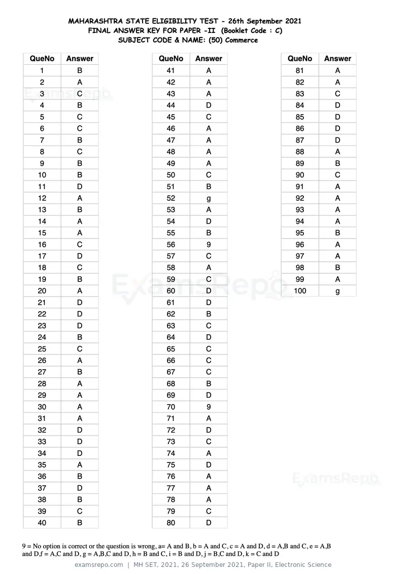
Text of page 107
MAHARASHTRA STATE ELIGIBILITY TEST - 26th September 2021
                    FINAL ANSWER KEY FOR PAPER -II (Booklet Code : C)
                           SUBJECT CODE & NAME: (50) Commerce

  QueNo        Answer                            QueNo        Answer                           QueNo        Answer
      1            B                               41             A                               81              A
      2            A                               42             A                               82              A
      3            C                               43             A                               83              C
      4            B                               44             D                               84              D
      5            C                               45             C                               85              D
      6            C                               46             A                               86              D
      7            B                               47             A                               87              D
      8            C                               48             A                               88              A
      9            B                               49             A                               89              B
     10            B                               50             C                               90              C
     11            D                               51             B                               91              A
     12            A                               52             g                               92              A
     13            B                               53             A                               93              A
     14            A                               54             D                               94              A
     15            A                               55             B                               95              B
     16            C                               56             9                               96              A
     17            D                               57             C                               97              A
     18            C                               58             A                               98              B
     19            B                               59             C                               99              A
     20            A                               60             D                              100              g
     21            D                               61             D
     22            D                               62             B
     23            D                               63             C
     24            B                               64             D
     25            C                               65             C
     26            A                               66             C
     27            B                               67             C
     28            A                               68             B
     29            A                               69             D
     30            A                               70             9
     31            A                               71             A
     32            D                               72             D
     33            D                               73             C
     34            D                               74             A
     35            A                               75             D
     36            B                               76             A
     37            D                               77             A
     38            B                               78             A
     39            C                               79             C
     40            B                               80             D


9 = No option is correct or the question is wrong, a= A and B, b = A and C, c = A and D, d = A,B and C, e = A,B
and D,f = A,C and D, g = A,B,C and D, h = B and C, i = B and D, j = B,C and D, k = C and D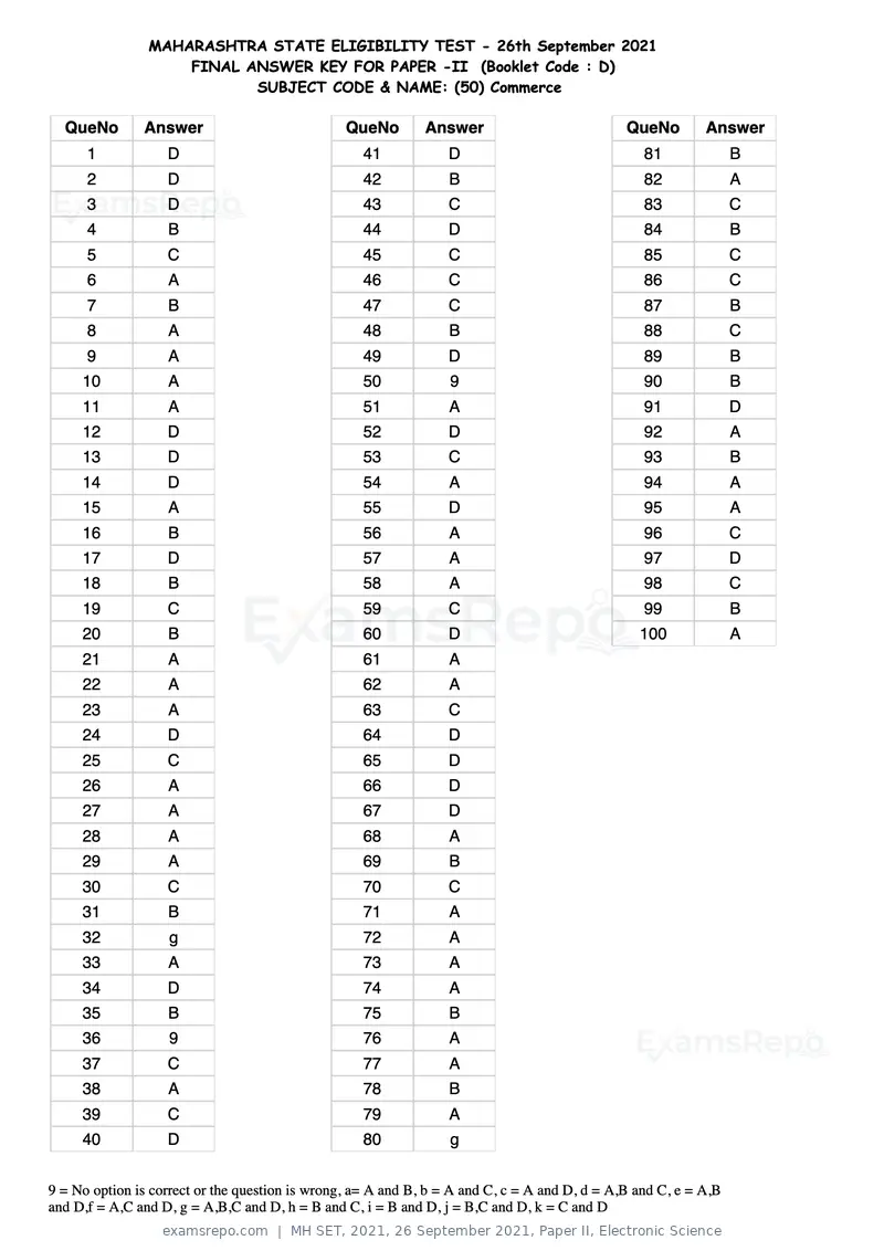
Text of page 108
MAHARASHTRA STATE ELIGIBILITY TEST - 26th September 2021
                    FINAL ANSWER KEY FOR PAPER -II (Booklet Code : D)
                           SUBJECT CODE & NAME: (50) Commerce

  QueNo        Answer                            QueNo        Answer                           QueNo        Answer
      1            D                               41             D                               81              B
      2            D                               42             B                               82              A
      3            D                               43             C                               83              C
      4            B                               44             D                               84              B
      5            C                               45             C                               85              C
      6            A                               46             C                               86              C
      7            B                               47             C                               87              B
      8            A                               48             B                               88              C
      9            A                               49             D                               89              B
     10            A                               50             9                               90              B
     11            A                               51             A                               91              D
     12            D                               52             D                               92              A
     13            D                               53             C                               93              B
     14            D                               54             A                               94              A
     15            A                               55             D                               95              A
     16            B                               56             A                               96              C
     17            D                               57             A                               97              D
     18            B                               58             A                               98              C
     19            C                               59             C                               99              B
     20            B                               60             D                              100              A
     21            A                               61             A
     22            A                               62             A
     23            A                               63             C
     24            D                               64             D
     25            C                               65             D
     26            A                               66             D
     27            A                               67             D
     28            A                               68             A
     29            A                               69             B
     30            C                               70             C
     31            B                               71             A
     32            g                               72             A
     33            A                               73             A
     34            D                               74             A
     35            B                               75             B
     36            9                               76             A
     37            C                               77             A
     38            A                               78             B
     39            C                               79             A
     40            D                               80             g


9 = No option is correct or the question is wrong, a= A and B, b = A and C, c = A and D, d = A,B and C, e = A,B
and D,f = A,C and D, g = A,B,C and D, h = B and C, i = B and D, j = B,C and D, k = C and D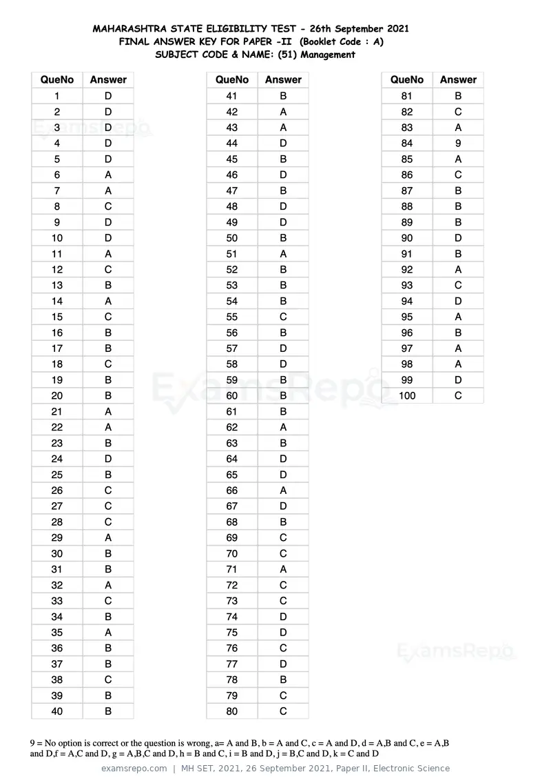
Text of page 109
MAHARASHTRA STATE ELIGIBILITY TEST - 26th September 2021
                    FINAL ANSWER KEY FOR PAPER -II (Booklet Code : A)
                          SUBJECT CODE & NAME: (51) Management

  QueNo        Answer                            QueNo        Answer                           QueNo        Answer
      1            D                               41             B                               81              B
      2            D                               42             A                               82              C
      3            D                               43             A                               83              A
      4            D                               44             D                               84              9
      5            D                               45             B                               85              A
      6            A                               46             D                               86              C
      7            A                               47             B                               87              B
      8            C                               48             D                               88              B
      9            D                               49             D                               89              B
     10            D                               50             B                               90              D
     11            A                               51             A                               91              B
     12            C                               52             B                               92              A
     13            B                               53             B                               93              C
     14            A                               54             B                               94              D
     15            C                               55             C                               95              A
     16            B                               56             B                               96              B
     17            B                               57             D                               97              A
     18            C                               58             D                               98              A
     19            B                               59             B                               99              D
     20            B                               60             B                              100              C
     21            A                               61             B
     22            A                               62             A
     23            B                               63             B
     24            D                               64             D
     25            B                               65             D
     26            C                               66             A
     27            C                               67             D
     28            C                               68             B
     29            A                               69             C
     30            B                               70             C
     31            B                               71             A
     32            A                               72             C
     33            C                               73             C
     34            B                               74             D
     35            A                               75             D
     36            B                               76             C
     37            B                               77             D
     38            C                               78             B
     39            B                               79             C
     40            B                               80             C


9 = No option is correct or the question is wrong, a= A and B, b = A and C, c = A and D, d = A,B and C, e = A,B
and D,f = A,C and D, g = A,B,C and D, h = B and C, i = B and D, j = B,C and D, k = C and D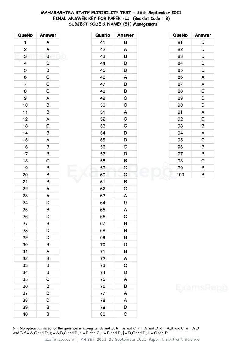
Text of page 110
MAHARASHTRA STATE ELIGIBILITY TEST - 26th September 2021
                    FINAL ANSWER KEY FOR PAPER -II (Booklet Code : B)
                          SUBJECT CODE & NAME: (51) Management

  QueNo        Answer                            QueNo        Answer                           QueNo        Answer
      1            A                               41             B                               81              D
      2            A                               42             A                               82              D
      3            B                               43             B                               83              D
      4            D                               44             D                               84              D
      5            B                               45             D                               85              D
      6            C                               46             A                               86              A
      7            C                               47             D                               87              A
      8            C                               48             B                               88              C
      9            A                               49             C                               89              D
     10            B                               50             C                               90              D
     11            B                               51             A                               91              A
     12            A                               52             C                               92              C
     13            C                               53             C                               93              B
     14            B                               54             D                               94              A
     15            A                               55             D                               95              C
     16            B                               56             C                               96              B
     17            B                               57             D                               97              B
     18            C                               58             B                               98              C
     19            B                               59             C                               99              B
     20            B                               60             C                              100              B
     21            B                               61             B
     22            A                               62             C
     23            A                               63             A
     24            D                               64             9
     25            B                               65             A
     26            D                               66             C
     27            B                               67             B
     28            D                               68             B
     29            D                               69             B
     30            B                               70             D
     31            A                               71             B
     32            B                               72             A
     33            B                               73             C
     34            B                               74             D
     35            C                               75             A
     36            B                               76             B
     37            D                               77             A
     38            D                               78             A
     39            B                               79             D
     40            B                               80             C


9 = No option is correct or the question is wrong, a= A and B, b = A and C, c = A and D, d = A,B and C, e = A,B
and D,f = A,C and D, g = A,B,C and D, h = B and C, i = B and D, j = B,C and D, k = C and D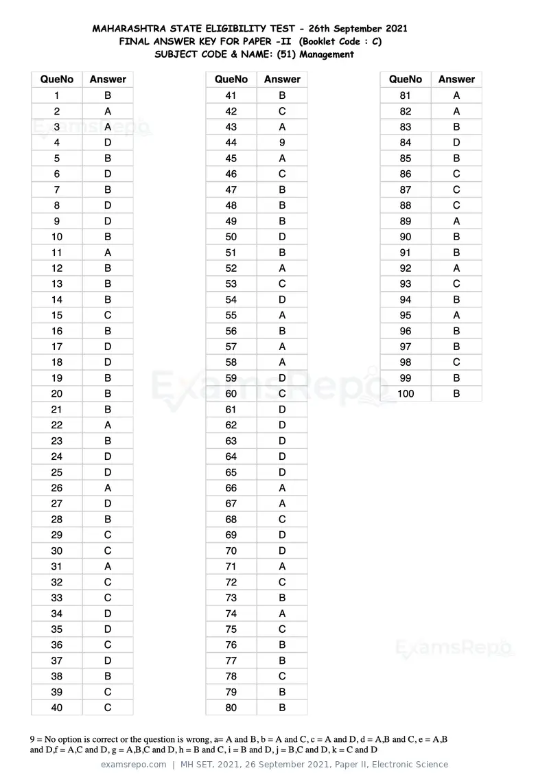
Text of page 111
MAHARASHTRA STATE ELIGIBILITY TEST - 26th September 2021
                    FINAL ANSWER KEY FOR PAPER -II (Booklet Code : C)
                          SUBJECT CODE & NAME: (51) Management

  QueNo        Answer                            QueNo        Answer                           QueNo        Answer
      1            B                               41             B                               81              A
      2            A                               42             C                               82              A
      3            A                               43             A                               83              B
      4            D                               44             9                               84              D
      5            B                               45             A                               85              B
      6            D                               46             C                               86              C
      7            B                               47             B                               87              C
      8            D                               48             B                               88              C
      9            D                               49             B                               89              A
     10            B                               50             D                               90              B
     11            A                               51             B                               91              B
     12            B                               52             A                               92              A
     13            B                               53             C                               93              C
     14            B                               54             D                               94              B
     15            C                               55             A                               95              A
     16            B                               56             B                               96              B
     17            D                               57             A                               97              B
     18            D                               58             A                               98              C
     19            B                               59             D                               99              B
     20            B                               60             C                              100              B
     21            B                               61             D
     22            A                               62             D
     23            B                               63             D
     24            D                               64             D
     25            D                               65             D
     26            A                               66             A
     27            D                               67             A
     28            B                               68             C
     29            C                               69             D
     30            C                               70             D
     31            A                               71             A
     32            C                               72             C
     33            C                               73             B
     34            D                               74             A
     35            D                               75             C
     36            C                               76             B
     37            D                               77             B
     38            B                               78             C
     39            C                               79             B
     40            C                               80             B


9 = No option is correct or the question is wrong, a= A and B, b = A and C, c = A and D, d = A,B and C, e = A,B
and D,f = A,C and D, g = A,B,C and D, h = B and C, i = B and D, j = B,C and D, k = C and D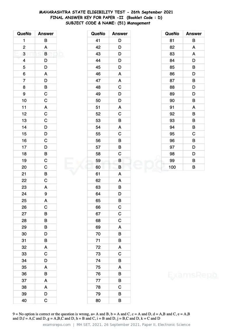
Text of page 112
MAHARASHTRA STATE ELIGIBILITY TEST - 26th September 2021
                    FINAL ANSWER KEY FOR PAPER -II (Booklet Code : D)
                          SUBJECT CODE & NAME: (51) Management

  QueNo        Answer                            QueNo        Answer                           QueNo        Answer
      1            B                               41             D                               81              B
      2            A                               42             D                               82              A
      3            B                               43             D                               83              A
      4            D                               44             D                               84              D
      5            D                               45             D                               85              B
      6            A                               46             A                               86              D
      7            D                               47             A                               87              B
      8            B                               48             C                               88              D
      9            C                               49             D                               89              D
     10            C                               50             D                               90              B
     11            A                               51             A                               91              A
     12            C                               52             C                               92              B
     13            C                               53             B                               93              B
     14            D                               54             A                               94              B
     15            D                               55             C                               95              C
     16            C                               56             B                               96              B
     17            D                               57             B                               97              D
     18            B                               58             C                               98              D
     19            C                               59             B                               99              B
     20            C                               60             B                              100              B
     21            B                               61             A
     22            C                               62             A
     23            A                               63             B
     24            9                               64             D
     25            A                               65             B
     26            C                               66             C
     27            B                               67             C
     28            B                               68             C
     29            B                               69             A
     30            D                               70             B
     31            B                               71             B
     32            A                               72             A
     33            C                               73             C
     34            D                               74             B
     35            A                               75             A
     36            B                               76             B
     37            A                               77             B
     38            A                               78             C
     39            D                               79             B
     40            C                               80             B


9 = No option is correct or the question is wrong, a= A and B, b = A and C, c = A and D, d = A,B and C, e = A,B
and D,f = A,C and D, g = A,B,C and D, h = B and C, i = B and D, j = B,C and D, k = C and D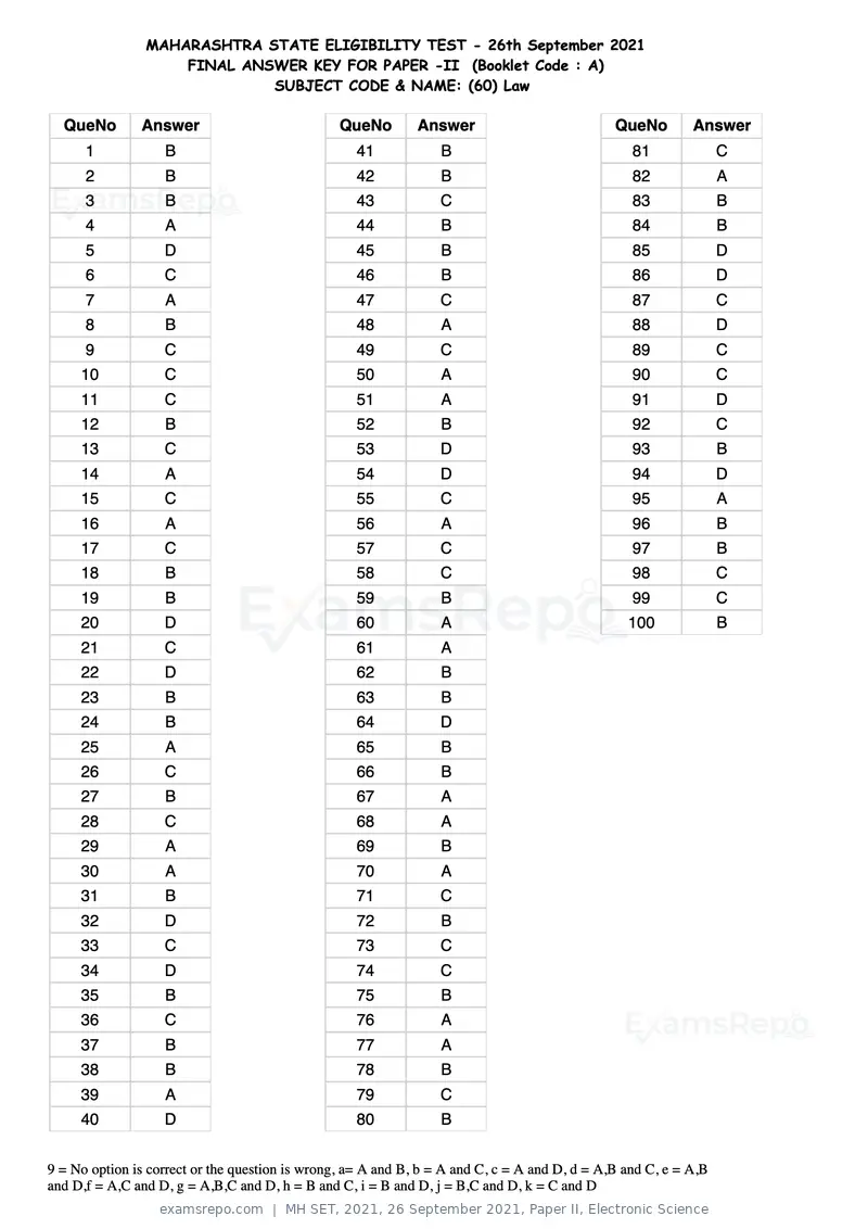
Text of page 113
MAHARASHTRA STATE ELIGIBILITY TEST - 26th September 2021
                    FINAL ANSWER KEY FOR PAPER -II (Booklet Code : A)
                             SUBJECT CODE & NAME: (60) Law

  QueNo        Answer                            QueNo        Answer                           QueNo        Answer
      1            B                               41             B                               81              C
      2            B                               42             B                               82              A
      3            B                               43             C                               83              B
      4            A                               44             B                               84              B
      5            D                               45             B                               85              D
      6            C                               46             B                               86              D
      7            A                               47             C                               87              C
      8            B                               48             A                               88              D
      9            C                               49             C                               89              C
     10            C                               50             A                               90              C
     11            C                               51             A                               91              D
     12            B                               52             B                               92              C
     13            C                               53             D                               93              B
     14            A                               54             D                               94              D
     15            C                               55             C                               95              A
     16            A                               56             A                               96              B
     17            C                               57             C                               97              B
     18            B                               58             C                               98              C
     19            B                               59             B                               99              C
     20            D                               60             A                              100              B
     21            C                               61             A
     22            D                               62             B
     23            B                               63             B
     24            B                               64             D
     25            A                               65             B
     26            C                               66             B
     27            B                               67             A
     28            C                               68             A
     29            A                               69             B
     30            A                               70             A
     31            B                               71             C
     32            D                               72             B
     33            C                               73             C
     34            D                               74             C
     35            B                               75             B
     36            C                               76             A
     37            B                               77             A
     38            B                               78             B
     39            A                               79             C
     40            D                               80             B


9 = No option is correct or the question is wrong, a= A and B, b = A and C, c = A and D, d = A,B and C, e = A,B
and D,f = A,C and D, g = A,B,C and D, h = B and C, i = B and D, j = B,C and D, k = C and D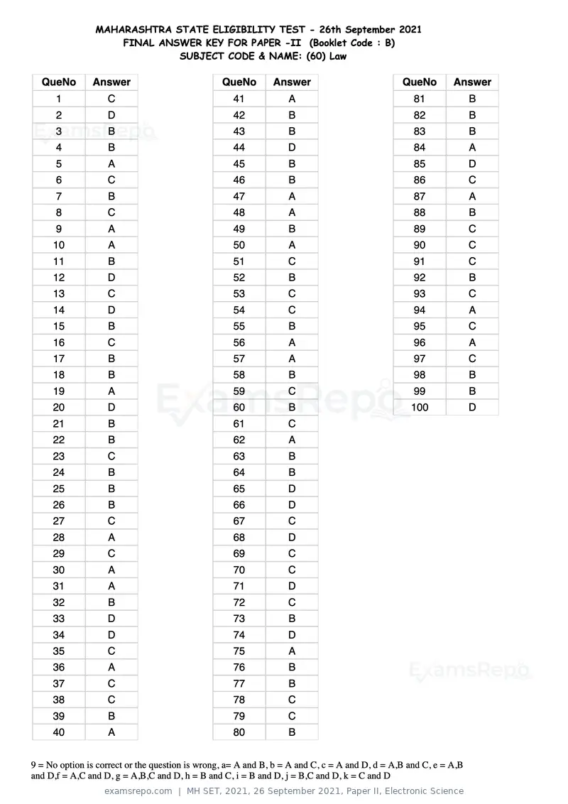
Text of page 114
MAHARASHTRA STATE ELIGIBILITY TEST - 26th September 2021
                    FINAL ANSWER KEY FOR PAPER -II (Booklet Code : B)
                             SUBJECT CODE & NAME: (60) Law

  QueNo        Answer                            QueNo        Answer                           QueNo        Answer
      1            C                               41             A                               81              B
      2            D                               42             B                               82              B
      3            B                               43             B                               83              B
      4            B                               44             D                               84              A
      5            A                               45             B                               85              D
      6            C                               46             B                               86              C
      7            B                               47             A                               87              A
      8            C                               48             A                               88              B
      9            A                               49             B                               89              C
     10            A                               50             A                               90              C
     11            B                               51             C                               91              C
     12            D                               52             B                               92              B
     13            C                               53             C                               93              C
     14            D                               54             C                               94              A
     15            B                               55             B                               95              C
     16            C                               56             A                               96              A
     17            B                               57             A                               97              C
     18            B                               58             B                               98              B
     19            A                               59             C                               99              B
     20            D                               60             B                              100              D
     21            B                               61             C
     22            B                               62             A
     23            C                               63             B
     24            B                               64             B
     25            B                               65             D
     26            B                               66             D
     27            C                               67             C
     28            A                               68             D
     29            C                               69             C
     30            A                               70             C
     31            A                               71             D
     32            B                               72             C
     33            D                               73             B
     34            D                               74             D
     35            C                               75             A
     36            A                               76             B
     37            C                               77             B
     38            C                               78             C
     39            B                               79             C
     40            A                               80             B


9 = No option is correct or the question is wrong, a= A and B, b = A and C, c = A and D, d = A,B and C, e = A,B
and D,f = A,C and D, g = A,B,C and D, h = B and C, i = B and D, j = B,C and D, k = C and D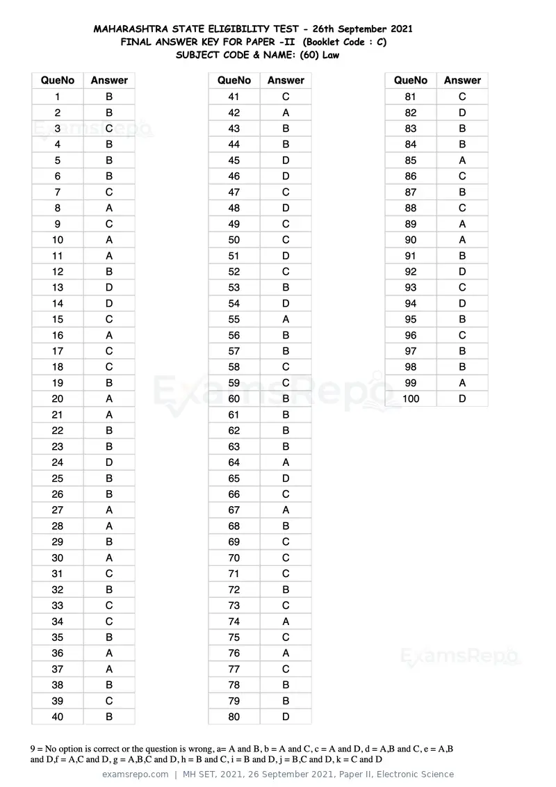
Text of page 115
MAHARASHTRA STATE ELIGIBILITY TEST - 26th September 2021
                    FINAL ANSWER KEY FOR PAPER -II (Booklet Code : C)
                             SUBJECT CODE & NAME: (60) Law

  QueNo        Answer                            QueNo        Answer                           QueNo        Answer
      1            B                               41             C                               81              C
      2            B                               42             A                               82              D
      3            C                               43             B                               83              B
      4            B                               44             B                               84              B
      5            B                               45             D                               85              A
      6            B                               46             D                               86              C
      7            C                               47             C                               87              B
      8            A                               48             D                               88              C
      9            C                               49             C                               89              A
     10            A                               50             C                               90              A
     11            A                               51             D                               91              B
     12            B                               52             C                               92              D
     13            D                               53             B                               93              C
     14            D                               54             D                               94              D
     15            C                               55             A                               95              B
     16            A                               56             B                               96              C
     17            C                               57             B                               97              B
     18            C                               58             C                               98              B
     19            B                               59             C                               99              A
     20            A                               60             B                              100              D
     21            A                               61             B
     22            B                               62             B
     23            B                               63             B
     24            D                               64             A
     25            B                               65             D
     26            B                               66             C
     27            A                               67             A
     28            A                               68             B
     29            B                               69             C
     30            A                               70             C
     31            C                               71             C
     32            B                               72             B
     33            C                               73             C
     34            C                               74             A
     35            B                               75             C
     36            A                               76             A
     37            A                               77             C
     38            B                               78             B
     39            C                               79             B
     40            B                               80             D


9 = No option is correct or the question is wrong, a= A and B, b = A and C, c = A and D, d = A,B and C, e = A,B
and D,f = A,C and D, g = A,B,C and D, h = B and C, i = B and D, j = B,C and D, k = C and D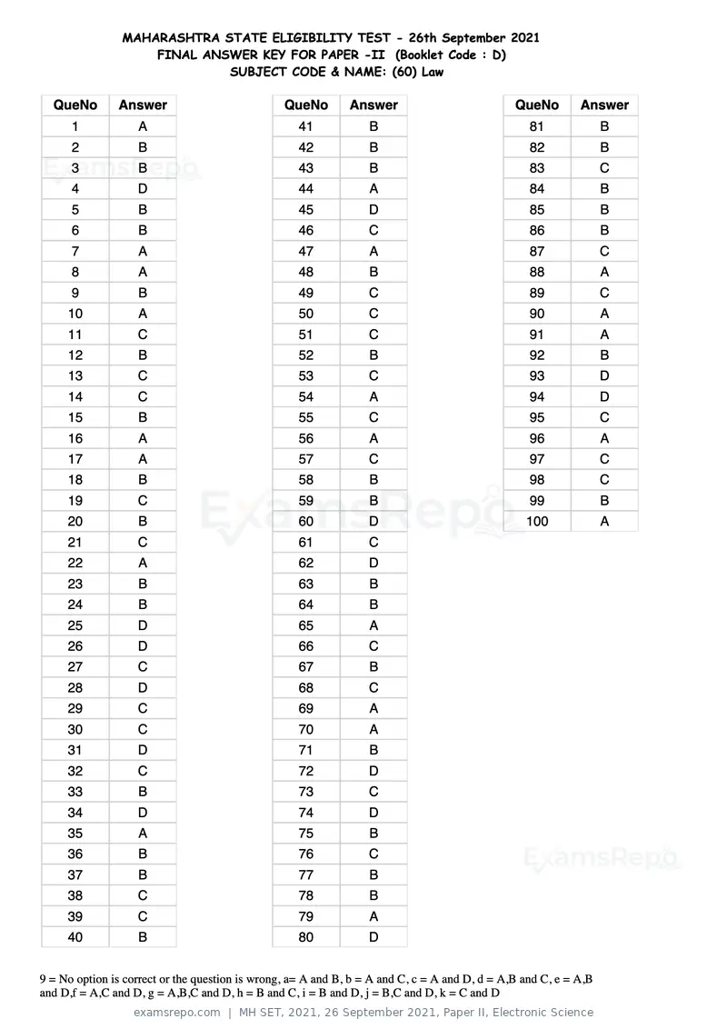
Text of page 116
MAHARASHTRA STATE ELIGIBILITY TEST - 26th September 2021
                    FINAL ANSWER KEY FOR PAPER -II (Booklet Code : D)
                             SUBJECT CODE & NAME: (60) Law

  QueNo        Answer                            QueNo        Answer                           QueNo        Answer
      1            A                               41             B                               81              B
      2            B                               42             B                               82              B
      3            B                               43             B                               83              C
      4            D                               44             A                               84              B
      5            B                               45             D                               85              B
      6            B                               46             C                               86              B
      7            A                               47             A                               87              C
      8            A                               48             B                               88              A
      9            B                               49             C                               89              C
     10            A                               50             C                               90              A
     11            C                               51             C                               91              A
     12            B                               52             B                               92              B
     13            C                               53             C                               93              D
     14            C                               54             A                               94              D
     15            B                               55             C                               95              C
     16            A                               56             A                               96              A
     17            A                               57             C                               97              C
     18            B                               58             B                               98              C
     19            C                               59             B                               99              B
     20            B                               60             D                              100              A
     21            C                               61             C
     22            A                               62             D
     23            B                               63             B
     24            B                               64             B
     25            D                               65             A
     26            D                               66             C
     27            C                               67             B
     28            D                               68             C
     29            C                               69             A
     30            C                               70             A
     31            D                               71             B
     32            C                               72             D
     33            B                               73             C
     34            D                               74             D
     35            A                               75             B
     36            B                               76             C
     37            B                               77             B
     38            C                               78             B
     39            C                               79             A
     40            B                               80             D


9 = No option is correct or the question is wrong, a= A and B, b = A and C, c = A and D, d = A,B and C, e = A,B
and D,f = A,C and D, g = A,B,C and D, h = B and C, i = B and D, j = B,C and D, k = C and D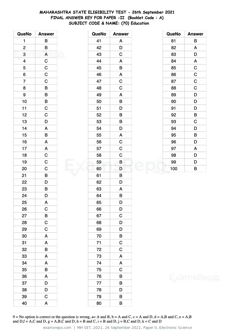
Text of page 117
MAHARASHTRA STATE ELIGIBILITY TEST - 26th September 2021
                    FINAL ANSWER KEY FOR PAPER -II (Booklet Code : A)
                           SUBJECT CODE & NAME: (70) Education

  QueNo        Answer                            QueNo        Answer                           QueNo        Answer
      1            B                               41             A                               81              B
      2            B                               42             D                               82              A
      3            A                               43             C                               83              D
      4            C                               44             A                               84              A
      5            C                               45             B                               85              C
      6            C                               46             A                               86              C
      7            C                               47             C                               87              C
      8            B                               48             C                               88              C
      9            B                               49             A                               89              D
     10            B                               50             B                               90              D
     11            C                               51             D                               91              D
     12            C                               52             B                               92              B
     13            D                               53             B                               93              C
     14            A                               54             D                               94              D
     15            B                               55             A                               95              B
     16            A                               56             C                               96              D
     17            A                               57             C                               97              A
     18            C                               58             C                               98              D
     19            C                               59             B                               99              D
     20            C                               60             D                              100              B
     21            B                               61             B
     22            D                               62             D
     23            B                               63             A
     24            D                               64             B
     25            A                               65             D
     26            C                               66             D
     27            B                               67             C
     28            C                               68             D
     29            C                               69             D
     30            A                               70             B
     31            A                               71             C
     32            B                               72             C
     33            A                               73             A
     34            A                               74             A
     35            B                               75             C
     36            A                               76             B
     37            D                               77             B
     38            D                               78             D
     39            C                               79             B
     40            A                               80             B


9 = No option is correct or the question is wrong, a= A and B, b = A and C, c = A and D, d = A,B and C, e = A,B
and D,f = A,C and D, g = A,B,C and D, h = B and C, i = B and D, j = B,C and D, k = C and D
Text of page 118
MAHARASHTRA STATE ELIGIBILITY TEST - 26th September 2021
                    FINAL ANSWER KEY FOR PAPER -II (Booklet Code : B)
                           SUBJECT CODE & NAME: (70) Education

  QueNo        Answer                            QueNo        Answer                           QueNo        Answer
      1            B                               41             B                               81              B
      2            D                               42             D                               82              B
      3            B                               43             A                               83              A
      4            D                               44             B                               84              C
      5            A                               45             D                               85              C
      6            C                               46             D                               86              C
      7            B                               47             C                               87              C
      8            C                               48             D                               88              B
      9            C                               49             D                               89              B
     10            A                               50             B                               90              B
     11            A                               51             C                               91              C
     12            B                               52             C                               92              C
     13            A                               53             A                               93              D
     14            A                               54             A                               94              A
     15            B                               55             C                               95              B
     16            A                               56             B                               96              A
     17            D                               57             B                               97              A
     18            D                               58             D                               98              C
     19            C                               59             B                               99              C
     20            A                               60             B                              100              C
     21            A                               61             B
     22            D                               62             A
     23            C                               63             D
     24            A                               64             A
     25            B                               65             C
     26            A                               66             C
     27            C                               67             C
     28            C                               68             C
     29            A                               69             D
     30            B                               70             D
     31            D                               71             D
     32            B                               72             B
     33            B                               73             C
     34            D                               74             D
     35            A                               75             B
     36            C                               76             D
     37            C                               77             A
     38            C                               78             D
     39            B                               79             D
     40            D                               80             B


9 = No option is correct or the question is wrong, a= A and B, b = A and C, c = A and D, d = A,B and C, e = A,B
and D,f = A,C and D, g = A,B,C and D, h = B and C, i = B and D, j = B,C and D, k = C and D
Text of page 119
MAHARASHTRA STATE ELIGIBILITY TEST - 26th September 2021
                    FINAL ANSWER KEY FOR PAPER -II (Booklet Code : C)
                           SUBJECT CODE & NAME: (70) Education

  QueNo        Answer                            QueNo        Answer                           QueNo        Answer
      1            A                               41             B                               81              B
      2            D                               42             A                               82              D
      3            C                               43             D                               83              B
      4            A                               44             A                               84              D
      5            B                               45             C                               85              A
      6            A                               46             C                               86              C
      7            C                               47             C                               87              B
      8            C                               48             C                               88              C
      9            A                               49             D                               89              C
     10            B                               50             D                               90              A
     11            D                               51             D                               91              A
     12            B                               52             B                               92              B
     13            B                               53             C                               93              A
     14            D                               54             D                               94              A
     15            A                               55             B                               95              B
     16            C                               56             D                               96              A
     17            C                               57             A                               97              D
     18            C                               58             D                               98              D
     19            B                               59             D                               99              C
     20            D                               60             B                              100              A
     21            B                               61             B
     22            D                               62             B
     23            A                               63             A
     24            B                               64             C
     25            D                               65             C
     26            D                               66             C
     27            C                               67             C
     28            D                               68             B
     29            D                               69             B
     30            B                               70             B
     31            C                               71             C
     32            C                               72             C
     33            A                               73             D
     34            A                               74             A
     35            C                               75             B
     36            B                               76             A
     37            B                               77             A
     38            D                               78             C
     39            B                               79             C
     40            B                               80             C


9 = No option is correct or the question is wrong, a= A and B, b = A and C, c = A and D, d = A,B and C, e = A,B
and D,f = A,C and D, g = A,B,C and D, h = B and C, i = B and D, j = B,C and D, k = C and D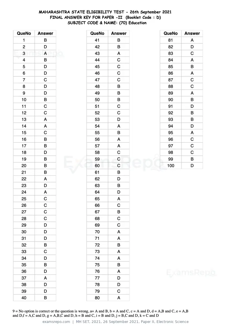
Text of page 120
MAHARASHTRA STATE ELIGIBILITY TEST - 26th September 2021
                    FINAL ANSWER KEY FOR PAPER -II (Booklet Code : D)
                           SUBJECT CODE & NAME: (70) Education

  QueNo        Answer                            QueNo        Answer                           QueNo        Answer
      1            B                               41             B                               81              A
      2            D                               42             B                               82              D
      3            A                               43             A                               83              C
      4            B                               44             C                               84              A
      5            D                               45             C                               85              B
      6            D                               46             C                               86              A
      7            C                               47             C                               87              C
      8            D                               48             B                               88              C
      9            D                               49             B                               89              A
     10            B                               50             B                               90              B
     11            C                               51             C                               91              D
     12            C                               52             C                               92              B
     13            A                               53             D                               93              B
     14            A                               54             A                               94              D
     15            C                               55             B                               95              A
     16            B                               56             A                               96              C
     17            B                               57             A                               97              C
     18            D                               58             C                               98              C
     19            B                               59             C                               99              B
     20            B                               60             C                              100              D
     21            B                               61             B
     22            A                               62             D
     23            D                               63             B
     24            A                               64             D
     25            C                               65             A
     26            C                               66             C
     27            C                               67             B
     28            C                               68             C
     29            D                               69             C
     30            D                               70             A
     31            D                               71             A
     32            B                               72             B
     33            C                               73             A
     34            D                               74             A
     35            B                               75             B
     36            D                               76             A
     37            A                               77             D
     38            D                               78             D
     39            D                               79             C
     40            B                               80             A


9 = No option is correct or the question is wrong, a= A and B, b = A and C, c = A and D, d = A,B and C, e = A,B
and D,f = A,C and D, g = A,B,C and D, h = B and C, i = B and D, j = B,C and D, k = C and D
Text of page 121
MAHARASHTRA STATE ELIGIBILITY TEST - 26th September 2021
                    FINAL ANSWER KEY FOR PAPER -II (Booklet Code : A)
                        SUBJECT CODE & NAME: (71) Physical Education

  QueNo        Answer                            QueNo        Answer                           QueNo        Answer
      1            C                               41             A                               81              A
      2            B                               42             B                               82              B
      3            C                               43             B                               83              A
      4            B                               44             A                               84              A
      5            D                               45             B                               85              B
      6            B                               46             A                               86              D
      7            A                               47             D                               87              C
      8            A                               48             D                               88              A
      9            A                               49             A                               89              C
     10            B                               50             B                               90              A
     11            C                               51             B                               91              B
     12            D                               52             C                               92              D
     13            B                               53             B                               93              C
     14            A                               54             A                               94              C
     15            C                               55             C                               95              C
     16            D                               56             C                               96              D
     17            C                               57             D                               97              C
     18            D                               58             C                               98              B
     19            B                               59             C                               99              A
     20            B                               60             C                              100              A
     21            A                               61             C
     22            A                               62             B
     23            B                               63             A
     24            C                               64             A
     25            B                               65             A
     26            A                               66             B
     27            C                               67             A
     28            D                               68             A
     29            B                               69             C
     30            A                               70             D
     31            D                               71             B
     32            C                               72             B
     33            B                               73             D
     34            A                               74             B
     35            A                               75             D
     36            B                               76             B
     37            A                               77             D
     38            B                               78             C
     39            B                               79             B
     40            B                               80             B


9 = No option is correct or the question is wrong, a= A and B, b = A and C, c = A and D, d = A,B and C, e = A,B
and D,f = A,C and D, g = A,B,C and D, h = B and C, i = B and D, j = B,C and D, k = C and D
Text of page 122
MAHARASHTRA STATE ELIGIBILITY TEST - 26th September 2021
                    FINAL ANSWER KEY FOR PAPER -II (Booklet Code : B)
                        SUBJECT CODE & NAME: (71) Physical Education

  QueNo        Answer                            QueNo        Answer                           QueNo        Answer
      1            A                               41             C                               81              C
      2            A                               42             B                               82              B
      3            B                               43             A                               83              C
      4            C                               44             A                               84              B
      5            B                               45             A                               85              D
      6            A                               46             B                               86              B
      7            C                               47             A                               87              A
      8            D                               48             A                               88              A
      9            B                               49             C                               89              A
     10            A                               50             D                               90              B
     11            D                               51             B                               91              C
     12            C                               52             B                               92              D
     13            B                               53             D                               93              B
     14            A                               54             B                               94              A
     15            A                               55             D                               95              C
     16            B                               56             B                               96              D
     17            A                               57             D                               97              C
     18            B                               58             C                               98              D
     19            B                               59             B                               99              B
     20            B                               60             B                              100              B
     21            A                               61             A
     22            B                               62             B
     23            B                               63             A
     24            A                               64             A
     25            B                               65             B
     26            A                               66             D
     27            D                               67             C
     28            D                               68             A
     29            A                               69             C
     30            B                               70             A
     31            B                               71             B
     32            C                               72             D
     33            B                               73             C
     34            A                               74             C
     35            C                               75             C
     36            C                               76             D
     37            D                               77             C
     38            C                               78             B
     39            C                               79             A
     40            C                               80             A


9 = No option is correct or the question is wrong, a= A and B, b = A and C, c = A and D, d = A,B and C, e = A,B
and D,f = A,C and D, g = A,B,C and D, h = B and C, i = B and D, j = B,C and D, k = C and D
Text of page 123
MAHARASHTRA STATE ELIGIBILITY TEST - 26th September 2021
                    FINAL ANSWER KEY FOR PAPER -II (Booklet Code : C)
                        SUBJECT CODE & NAME: (71) Physical Education

  QueNo        Answer                            QueNo        Answer                           QueNo        Answer
      1            A                               41             A                               81              A
      2            B                               42             B                               82              A
      3            B                               43             A                               83              B
      4            A                               44             A                               84              C
      5            B                               45             B                               85              B
      6            A                               46             D                               86              A
      7            D                               47             C                               87              C
      8            D                               48             A                               88              D
      9            A                               49             C                               89              B
     10            B                               50             A                               90              A
     11            B                               51             B                               91              D
     12            C                               52             D                               92              C
     13            B                               53             C                               93              B
     14            A                               54             C                               94              A
     15            C                               55             C                               95              A
     16            C                               56             D                               96              B
     17            D                               57             C                               97              A
     18            C                               58             B                               98              B
     19            C                               59             A                               99              B
     20            C                               60             A                              100              B
     21            C                               61             C
     22            B                               62             B
     23            A                               63             C
     24            A                               64             B
     25            A                               65             D
     26            B                               66             B
     27            A                               67             A
     28            A                               68             A
     29            C                               69             A
     30            D                               70             B
     31            B                               71             C
     32            B                               72             D
     33            D                               73             B
     34            B                               74             A
     35            D                               75             C
     36            B                               76             D
     37            D                               77             C
     38            C                               78             D
     39            B                               79             B
     40            B                               80             B


9 = No option is correct or the question is wrong, a= A and B, b = A and C, c = A and D, d = A,B and C, e = A,B
and D,f = A,C and D, g = A,B,C and D, h = B and C, i = B and D, j = B,C and D, k = C and D
Text of page 124
MAHARASHTRA STATE ELIGIBILITY TEST - 26th September 2021
                    FINAL ANSWER KEY FOR PAPER -II (Booklet Code : D)
                        SUBJECT CODE & NAME: (71) Physical Education

  QueNo        Answer                            QueNo        Answer                           QueNo        Answer
      1            C                               41             C                               81              A
      2            B                               42             B                               82              B
      3            A                               43             C                               83              B
      4            A                               44             B                               84              A
      5            A                               45             D                               85              B
      6            B                               46             B                               86              A
      7            A                               47             A                               87              D
      8            A                               48             A                               88              D
      9            C                               49             A                               89              A
     10            D                               50             B                               90              B
     11            B                               51             C                               91              B
     12            B                               52             D                               92              C
     13            D                               53             B                               93              B
     14            B                               54             A                               94              A
     15            D                               55             C                               95              C
     16            B                               56             D                               96              C
     17            D                               57             C                               97              D
     18            C                               58             D                               98              C
     19            B                               59             B                               99              C
     20            B                               60             B                              100              C
     21            A                               61             A
     22            B                               62             A
     23            A                               63             B
     24            A                               64             C
     25            B                               65             B
     26            D                               66             A
     27            C                               67             C
     28            A                               68             D
     29            C                               69             B
     30            A                               70             A
     31            B                               71             D
     32            D                               72             C
     33            C                               73             B
     34            C                               74             A
     35            C                               75             A
     36            D                               76             B
     37            C                               77             A
     38            B                               78             B
     39            A                               79             B
     40            A                               80             B


9 = No option is correct or the question is wrong, a= A and B, b = A and C, c = A and D, d = A,B and C, e = A,B
and D,f = A,C and D, g = A,B,C and D, h = B and C, i = B and D, j = B,C and D, k = C and D
Page 1 of 32
Source: Savitribai Phule Pune University. Question paper published by Savitribai Phule Pune University.