
Machine-translated by Google. Questions are authored in English.
Top

Field Effect Transistors Questions and Answers

121.

Consider the following four transistors :

1. CE mode
2. CC mode
3. MOSFET
4. FET
The correct order in which, the input impedance increases is

Exam Year(s)

UGC NET - 2012,

Answer: A

The input impedance rises in the order CE, CC, FET and MOSFET, which is 1, 2, 4, 3 (option A). A common-emitter stage has an input resistance of the order of a kilohm, a common-collector stage (emitter follower) about a hundred kilohm, a JFET about \(10^8\) ohm, and an insulated-gate MOSFET \(10^{10}\) ohm or more.

Options B and C put the MOSFET before the FET, and option D reverses the whole order.

Please log in or register to report this question.
122.

In a JFET, the amplification factor \(\mu\), transconductance \(g_m\) and the dynamic drain resistance \(v_d\) are related as

Exam Year(s)

UGC NET - 2012,

Answer: C

In a JFET the amplification factor is the product of the transconductance and the dynamic drain resistance, \(\mu = g_m \cdot v_d\). It follows from the definitions: \(g_m\) is the change in drain current per unit change in gate voltage at constant drain voltage, \(v_d\) (the drain resistance \(r_d\)) is the change in drain voltage per unit change in drain current at constant gate voltage, and \(\mu\) is the change in drain voltage per unit change in gate voltage at constant drain current. Multiplying the first two gives the third, because the drain current terms cancel.


The ratios \(g_m/v_d\) and \(v_d/g_m\) have the wrong units, since they are not dimensionless, and \(g_m v_d^{2}\) does not have the units of a pure ratio either. The answer is \(\mu = g_m \cdot v_d\).

Please log in or register to report this question.

123.

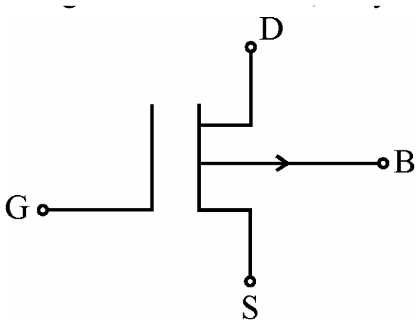
The figure shown below, is symbol of

Circuit symbol of a MOSFET with drain D at the top, source S at the bottom, gate G at the left drawn as a plate separated by a gap from a continuous channel line, and a body terminal B at the right with an arrow pointing away from the channel.

Exam Year(s)

UGC NET - 2012,

Answer: A

The symbol is that of a P-channel depletion MOSFET. Two features of the drawing decide this. The channel is drawn as one continuous line next to the gate plate, which marks a depletion type, since a channel already exists with no gate voltage; an enhancement device draws the channel as three broken segments. The arrow on the body terminal B points away from the channel, which is the convention for a P-channel device, while an arrow pointing into the channel marks an N-channel device.


The enhancement option is therefore wrong because the channel is not broken, the complementary MOSFET would show two transistors, and a JFET symbol has no insulated gate plate. The answer is P-channel depletion MOSFET.

Please log in or register to report this question.

124.

Which of the following is/are valid statement(s) ?

I. AJFET has one built-in diode.
II. AJFET has two built-in diode.
III. The pinch off voltage of a JFET has same magnitude as that of gate voltage.
IV. A JFET is a voltage controlled device.

Exam Year(s)

UGC NET - 2012,

Answer: B

The valid statements are II, III and IV. A JFET has two p-n junctions between the gate and the channel, so it has two built-in diodes and not one, which makes statement I wrong and statement II right. The pinch-off voltage is the gate-source voltage that closes the channel, so it has the same magnitude as the gate cut-off voltage, and statement III is right. The drain current is controlled by the gate voltage, so it is a voltage controlled device, and statement IV is right. The option with I, III and IV fails because of statement I, and the options without III or IV leave out true statements. The answer is II, III, IV.

Please log in or register to report this question.

125.

In a JFET the change in drain current is due to the applied

Exam Year(s)

UGC NET - 2012,

Answer: B

In a JFET the drain current is controlled by the electric field between the gate and the source: the reverse-biased gate junction sets the width of the depletion region, which narrows or widens the conducting channel, so the drain current changes with the gate-to-source voltage. A magnetic field plays no part in the operation of the device, which rules out options C and D. The electric field between source and drain drives the current along the channel, but it is not the controlling quantity that the question asks about, so option A is also wrong. The answer is option B.

Please log in or register to report this question.

126.

Consider an n-channel depletion mode MOSFET having following parameters :

\(V_{TN} = -2.5\) V and \(K_{n} = 1.1\) mA/V\(^{2}\)

If \(V_{GS} = 0\)V and \(V_{DS} = 0.5\) V, then current \(I_{D}\), is

Exam Year(s)

UGC NET - 2012,

Answer: C

The drain current is 2.48 mA, option (C). With \(V_{GS} = 0\) and \(V_{TN} = -2.5\) V, the overdrive is \(V_{GS} - V_{TN} = 2.5\) V. As \(V_{DS} = 0.5\) V is less than 2.5 V, the device works in the triode region, where

\[ I_{D} = K_{n}\left[2(V_{GS}-V_{TN})V_{DS}\right.\]

\[ \left. -\,V_{DS}^{2}\right] \]

\[ I_{D} = 1.1\left[2(2.5)(0.5) - 0.25\right] \]

\[ = 1.1\times2.25 = 2.48\ \text{mA} \]

Options (A), (B) and (D) are not given by the triode equation. The saturation formula \(K_{n}(V_{GS}-V_{TN})^{2}\), which would give 6.9 mA, applies only when \(V_{DS}\) is at least 2.5 V, which is not the case here.

Please log in or register to report this question.

127.

In a JFET, the amplification factor \(\mu\), transconductance \(g_{m}\), and the dynamic drain resistance (\(r_{d}\)) are related as

Exam Year(s)

UGC NET - 2013,

Answer: C

The three JFET parameters are related by \(\mu = r_{d} \times g_{m}\), which is option (C). The amplification factor is the ratio of a change in drain-source voltage to the change in gate-source voltage that keeps the drain current constant, so

\[ \begin{aligned} \mu &= -\frac{\Delta V_{DS}}{\Delta V_{GS}} \\ &= \frac{\Delta V_{DS}}{\Delta I_{D}} \cdot \frac{\Delta I_{D}}{\Delta V_{GS}} \\ &= r_{d}\, g_{m} \end{aligned} \]

Options (A) and (B) are ratios, which have the wrong units for a dimensionless factor, and (D) squares the drain resistance, so the dimensions do not match either.

Please log in or register to report this question.

128.

The figure shown below, is symbol of

Circuit symbol of a MOSFET with gate G, drain D, source S and substrate B; the channel is drawn as a broken line and the substrate arrow points away from the channel

Exam Year(s)

UGC NET - 2013,

Answer: B

The symbol is that of a P-channel enhancement MOSFET, the second option. The channel is drawn as a broken line, which marks an enhancement type, in which no channel exists until the gate voltage forms it. The arrow on the substrate lead B points away from the channel, which is how a P-channel device is shown.

A depletion MOSFET would have an unbroken channel line, a JFET has no insulated gate and is drawn with a different gate symbol, and a complementary MOSFET shows both an n and a p device. So the other options do not fit.

Please log in or register to report this question.

129.

Consider the following devices :

1. BJT in CB mode
2. BJT in CE mode
3. JFET
4. MOSFET The correct sequence of these devices in increasing order of their impedance is

Exam Year(s)

UGC NET - 2013,

Answer: C

The increasing order of impedance is BJT in CB, BJT in CE, JFET, MOSFET, 1, 2, 3, 4, option (C).

A common base stage has a very low input impedance, a common emitter stage has a moderate one, a JFET has a high one because its gate junction is reverse biased, and a MOSFET has the highest because its gate is insulated by oxide.

Options (A) and (B) put the CE stage below the CB stage, and (B) and (D) put the JFET above the MOSFET, both of which reverse the order.

Please log in or register to report this question.

Loading…

Other Subjects

Tags: Field Effect Transistors Questions and Answers || Field Effect Transistors MCQ Questions and Answers || Field Effect Transistors GK Questions and Answers || Field Effect Transistors GK MCQ Questions || Field Effect Transistors Multiple Choice Questions and Answers || Field Effect Transistors GK || GK on Field Effect Transistors || Analog Electronics Questions and Answers || Analog Electronics MCQ Questions and Answers || Analog Electronics GK Questions and Answers || GK on Analog Electronics