
Machine-translated by Google. Questions are authored in English.
Top

Field Effect Transistors Questions and Answers

111.

In, ................. device the conductivity of a layer of a semiconductor is modulated by a transverse electric field.

Exam Year(s)

MH SET - 2023, SET Exam - 2023,

Answer: D

The device is the FET.

In a field-effect transistor the current flows through a channel, a thin layer of semiconductor, and the voltage on the gate sets up an electric field across (transverse to) that channel. The field changes the number of carriers in the channel, and so its conductivity, which is how the gate controls the drain current. The name 'field effect' comes from this mechanism.

A BJT is controlled by the injection of carriers across forward-biased junctions, with base current, not by a transverse field. A P-N diode and a Zener diode are two-terminal devices with no control electrode at all.

Please log in or register to report this question.

112.

What does the symbol IGSS represent in the context of a JFET ?

Exam Year(s)

MH SET - 2025, SET Exam - 2025,

Answer: D

IGSS is the gate current when the gate-source junction is reverse-biased.

In a JFET the gate-channel p-n junction is always operated in reverse bias. IGSS, the gate reverse current or gate leakage current, is the small current that flows into the gate with the drain shorted to the source and a specified reverse voltage applied between gate and source. It is typically in nanoamperes, which is why a JFET has a very high input resistance.

The drain current is ID (with IDSS its value at VGS = 0). The gate-source voltage is VGS. Forward-biasing the gate junction is avoided in normal operation and is not what IGSS specifies.

Please log in or register to report this question.
113.

Which of the following is true about the FET as its advantage ?

Exam Year(s)

MH SET - 2025, SET Exam - 2025,

Answer: D

The advantage is better thermal stability.

In a FET, current is carried by majority carriers only, and their mobility falls as temperature rises, so the drain current tends to decrease with heating. This negative temperature coefficient prevents thermal runaway, which can destroy a bipolar transistor. FETs also offer very high input resistance, low noise and small size.

A low input resistance is the opposite of the FET's main advantage, which is its very high input resistance, especially in MOSFETs. 'Big size, small life' is false, since FETs are compact and reliable. High output resistance is not usually listed as the FET's advantage over the BJT.

Please log in or register to report this question.

114.

The co-ordinates of the operating point (Q) for the following JFET circuit are ........

JFET circuit: VDD = +30 V; R1 = 2 megohm from VDD to the gate and R2 = 1 megohm from the gate to ground; drain to VDD through RD = 1 kilohm; source to ground through Rs = 2 kilohm

Exam Year(s)

MH SET - 2025, SET Exam - 2025,

Answer: D

The operating point is \(V_{DS} = 15\) V, \(I_{D} = 5\) mA.

The divider sets the gate voltage, and the source voltage is taken to sit at about the gate voltage (that is, \(V_{GS} \approx 0\), the approximation the options are built on):

\[ \begin{aligned} V_{G} &= 30 \times \frac{1\ \text{M}\Omega}{3\ \text{M}\Omega} = 10\ \text{V} \\ I_{D} &\approx \frac{V_{G}}{R_{s}} = \frac{10\ \text{V}}{2\ \text{k}\Omega} = 5\ \text{mA} \\ V_{DS} &= 30 - 5\ \text{mA}(1 + 2)\ \text{k}\Omega = 15\ \text{V} \end{aligned} \]

The other options put \(V_{DS}\) in millivolts. With 5 mA the two resistors drop only 15 V, which leaves 15 V, not 15 mV, across the transistor. Currents of 15 mA or 10 mA through the 3 kΩ of \(R_{D}\) and \(R_{s}\) would need 45 V or 30 V, more than or all of the supply, and are inconsistent with a 10 V gate.

Please log in or register to report this question.

115.

The drain current in a JFET is controlled by

Exam Year(s)

Tripura Public Service Commission - 2026,

Answer: B

The drain current in a JFET is controlled by the gate-source voltage.

The JFET is a voltage-controlled device. A reverse bias on the gate-source junction widens the depletion region into the channel, narrowing it and reducing the drain current. Shockley's equation gives the relation:

\[ I_D = I_{DSS}\left(1 - \frac{V_{GS}}{V_P}\right)^{2} \]

The gate is reverse biased, so gate current is almost zero and controls nothing. In saturation the drain voltage has little effect on the current. Source current is simply the drain current flowing out, a result rather than a control.

Please log in or register to report this question.

116.

For a JFET \(I_{DSS}\) = 8 mA and peak voltage \(V_p\) = -8 V, what will be the drain current for gate to source voltage of -2 V ?

Exam Year(s)

UGC NET - 2012,

Answer: A

The drain current is 4.5 mA (option A), from the JFET square-law relation in the saturation region.

\[ I_D = I_{DSS}\left(1 - \frac{V_{GS}}{V_p}\right)^2 \]

\[ I_D = 8\left(1 - \frac{-2}{-8}\right)^2 \]

\[ I_D = 8(0.75)^2 = 4.5\ \text{mA} \]

The value 8 mA (B) is the current at \(V_{GS} = 0\), where the bracket is 1. The values 16 mA and 12 mA are larger than \(I_{DSS}\), which a JFET cannot exceed at a gate voltage that reverse biases the channel.

Please log in or register to report this question.

117.

Consider the following four transistors :

1. CE mode
2. CC mode
3. MOSFET
4. FET
The correct order in which, the input impedance increases is

Exam Year(s)

UGC NET - 2012,

Answer: A

The input impedance rises in the order CE, CC, FET and MOSFET, which is 1, 2, 4, 3 (option A). A common-emitter stage has an input resistance of the order of a kilohm, a common-collector stage (emitter follower) about a hundred kilohm, a JFET about \(10^8\) ohm, and an insulated-gate MOSFET \(10^{10}\) ohm or more.

Options B and C put the MOSFET before the FET, and option D reverses the whole order.

Please log in or register to report this question.

118.

In a JFET, the amplification factor \(\mu\), transconductance \(g_m\) and the dynamic drain resistance \(v_d\) are related as

Exam Year(s)

UGC NET - 2012,

Answer: C

In a JFET the amplification factor is the product of the transconductance and the dynamic drain resistance, \(\mu = g_m \cdot v_d\). It follows from the definitions: \(g_m\) is the change in drain current per unit change in gate voltage at constant drain voltage, \(v_d\) (the drain resistance \(r_d\)) is the change in drain voltage per unit change in drain current at constant gate voltage, and \(\mu\) is the change in drain voltage per unit change in gate voltage at constant drain current. Multiplying the first two gives the third, because the drain current terms cancel.


The ratios \(g_m/v_d\) and \(v_d/g_m\) have the wrong units, since they are not dimensionless, and \(g_m v_d^{2}\) does not have the units of a pure ratio either. The answer is \(\mu = g_m \cdot v_d\).

Please log in or register to report this question.

119.

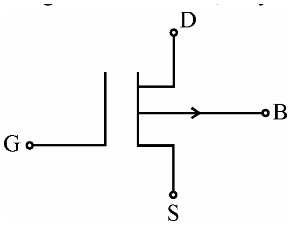
The figure shown below, is symbol of

Circuit symbol of a MOSFET with drain D at the top, source S at the bottom, gate G at the left drawn as a plate separated by a gap from a continuous channel line, and a body terminal B at the right with an arrow pointing away from the channel.

Exam Year(s)

UGC NET - 2012,

Answer: A

The symbol is that of a P-channel depletion MOSFET. Two features of the drawing decide this. The channel is drawn as one continuous line next to the gate plate, which marks a depletion type, since a channel already exists with no gate voltage; an enhancement device draws the channel as three broken segments. The arrow on the body terminal B points away from the channel, which is the convention for a P-channel device, while an arrow pointing into the channel marks an N-channel device.


The enhancement option is therefore wrong because the channel is not broken, the complementary MOSFET would show two transistors, and a JFET symbol has no insulated gate plate. The answer is P-channel depletion MOSFET.

Please log in or register to report this question.

120.

Which of the following is/are valid statement(s) ?

I. AJFET has one built-in diode.
II. AJFET has two built-in diode.
III. The pinch off voltage of a JFET has same magnitude as that of gate voltage.
IV. A JFET is a voltage controlled device.

Exam Year(s)

UGC NET - 2012,

Answer: B

The valid statements are II, III and IV. A JFET has two p-n junctions between the gate and the channel, so it has two built-in diodes and not one, which makes statement I wrong and statement II right. The pinch-off voltage is the gate-source voltage that closes the channel, so it has the same magnitude as the gate cut-off voltage, and statement III is right. The drain current is controlled by the gate voltage, so it is a voltage controlled device, and statement IV is right. The option with I, III and IV fails because of statement I, and the options without III or IV leave out true statements. The answer is II, III, IV.

Please log in or register to report this question.

Loading…

Other Subjects

Tags: Field Effect Transistors Questions and Answers || Field Effect Transistors MCQ Questions and Answers || Field Effect Transistors GK Questions and Answers || Field Effect Transistors GK MCQ Questions || Field Effect Transistors Multiple Choice Questions and Answers || Field Effect Transistors GK || GK on Field Effect Transistors || Analog Electronics Questions and Answers || Analog Electronics MCQ Questions and Answers || Analog Electronics GK Questions and Answers || GK on Analog Electronics