Machine-translated by Google. Questions are authored in English.
Top

Semiconductor Crystals Questions and Answers

1.

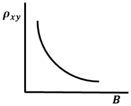
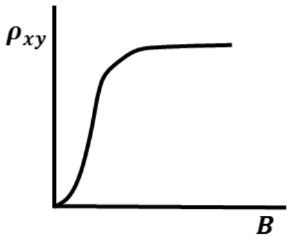
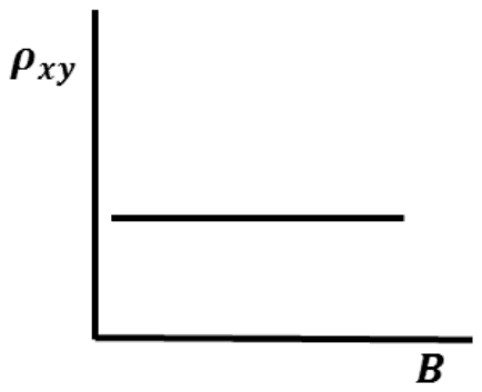
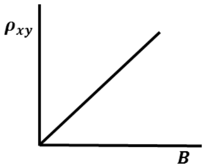
The Hall experiment is carried out with a non-magnetic semiconductor. The current \(I\) is along the \(x\)-axis and the magnetic field \(B\) is along the \(z\)-axis. Which one of the following is the CORRECT representation of the variation of the magnitude of the Hall resistivity \(\rho_{xy}\) as a function of the magnetic field?
Exam Year(s)

GATE Physics - 2023,

Answer: B

The Hall resistivity rises linearly with the magnetic field, the straight line through the origin in (B).

In steady state the Hall field balances the magnetic force on the carriers, giving \(E_{y} = v_{x}B = J_{x}B/(ne)\). So

\[ \rho_{xy} = \frac{E_{y}}{J_{x}} = \frac{B}{ne} \]

which is proportional to \(B\) and zero when there is no field. In a non-magnetic material there is no anomalous Hall contribution from a spontaneous magnetisation, so the line passes through the origin.

A constant (A) would mean a Hall signal at zero field; a falling curve (C) has the dependence upside down; and a curve that saturates into a plateau (D) resembles the quantum Hall or anomalous Hall behaviour, not the classical Hall effect asked about.

Please log in or register to report this question.
2.

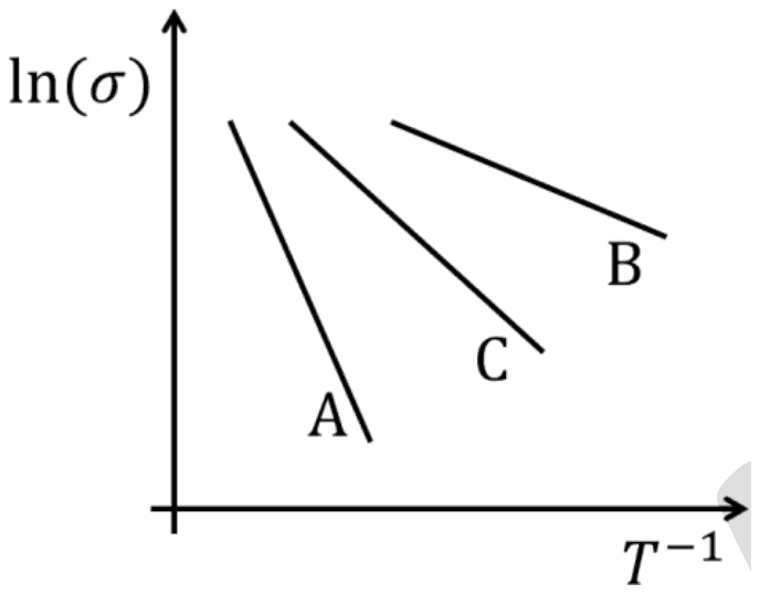
The temperature dependence of the electrical conductivity \((\sigma)\) of three intrinsic semiconductors A, B and C is shown in figure.

Plot of ln(sigma) against 1/T: three falling straight lines; A is the steepest, C is less steep and B is the least steep

Let EA, EB and EC be the bandgaps of A, B and C, respectively. Which one of the following relations is correct?

Exam Year(s)

GATE Physics - 2024,

Answer: D

The bandgaps satisfy EA > EC > EB.

For an intrinsic semiconductor the conductivity varies as

\[ \begin{aligned} \sigma &\propto e^{-E_{g}/2k_{B}T} \\ \ln\sigma &= \text{const} - \frac{E_{g}}{2k_{B}}\cdot\frac{1}{T} \end{aligned} \]

so on a plot of ln σ against 1/T the slope is -Eg/2kB. The steeper the line, the larger the bandgap. Line A is the steepest, C next and B the least steep.

The other orders mis-rank the slopes: putting C first, B first, or B above C would all require B or C to fall faster than the drawing shows.

Please log in or register to report this question.

3.

Consider an n-type silicon in which the fully ionized dopant concentration is \(10^{17}\ cm^{-3}\). The intrinsic electron density is \(1.5 \times 10^{10}\ cm^{-3}\). Which of the following options correctly states the equilibrium hole concentration in \(cm^{-3}\)?

Exam Year(s)

IIT JAM - 2026,

Answer: A

The equilibrium hole concentration is \(2.25 \times 10^{3}\ cm^{-3}\).

With all donors ionised, the electron concentration in the n-type silicon is the donor concentration, \(n = 10^{17}\ cm^{-3}\). At equilibrium the mass-action law fixes the product of electron and hole concentrations:

\[ \begin{aligned} np &= n_i^{2} \\ p &= \frac{(1.5 \times 10^{10})^{2}}{10^{17}} \\ &= \frac{2.25 \times 10^{20}}{10^{17}} = 2.25 \times 10^{3} \end{aligned} \]

Holes are the minority carriers, so their number is tiny compared with the \(10^{10}\) of intrinsic silicon: doping raises one carrier type and suppresses the other. The remaining options do not follow from \(n_i^2/N_D\) with these numbers.

Please log in or register to report this question.

4.

A phosphorous doped silicon semiconductor (doping density : 10\(^{17}\)/cm\(^{3}\)) is heated from 100°C to 200°C. Which one of the following statements is correct ?

Exam Year(s)

MH SET - 2019, SET Exam - 2019,

Answer: C

The correct statement is that the Fermi level moves towards the middle of the energy gap.

In n-type silicon the Fermi level lies near the conduction band at low temperature, because the donors supply most of the electrons. As the temperature rises, more electron-hole pairs are created across the gap, the material moves towards intrinsic behaviour, and the Fermi level moves down towards mid-gap.

The donor (phosphorus) level itself is fixed by the impurity, about 0.045 eV below the conduction band, and does not move with temperature, which rules out options B and D. Option A gives the wrong direction.

Please log in or register to report this question.

5.

In a p-type semiconductor, the Fermi level lies 0.4 eV above the valence band. If the concentration of the acceptor atoms is trippled and kT = 0.03 eV, the new position of the Fermi level will be :

Exam Year(s)

MH SET - 2020, SET Exam - 2020,

Answer: D

The Fermi level moves down to 0.367 eV above the valence band.

In a p-type semiconductor with full ionisation, \(p \approx N_{A}\) and \(E_{F} - E_{V} = kT\,\text{ln}(N_{V}/N_{A})\). Tripling \(N_{A}\) lowers this by \(kT\,\text{ln}\,3\):

\[ \begin{aligned} \Delta &= 0.03 \times \text{ln}\,3 = 0.03 \times 1.099 \\ &= 0.033\ \text{eV} \\ E_{F} - E_{V} &= 0.400 - 0.033 = 0.367\ \text{eV} \end{aligned} \]

More acceptors make the material more strongly p-type, so the Fermi level moves closer to the valence band, which rules out 0.525 eV. 0.250 eV and 0.100 eV are far too large a shift for a threefold change in doping.

Please log in or register to report this question.

6.

For an intrinsic semiconductor, \(m_{e}^{*}\) and \(m_{h}^{*}\) are respectively the effective masses of electrons and holes near the corresponding band edges. At a finite temperature, the position of the Fermi level :

Exam Year(s)

MH SET - 2023, SET Exam - 2023,

Answer: C

The Fermi level depends on both \(m_{e}^{*}\) and \(m_{h}^{*}\).

Setting the electron and hole concentrations equal in an intrinsic semiconductor gives

\[ \begin{aligned} E_{F} &= \frac{E_{c} + E_{v}}{2} \\ &+ \frac{3}{4}k_{B}T\ln\frac{m_{h}^{*}}{m_{e}^{*}} \end{aligned} \]

The effective masses enter through the effective densities of states of the two bands, and only their ratio matters. At T = 0 the Fermi level sits exactly at mid-gap, but at a finite temperature it shifts towards the band with the smaller density of states, so it depends on both masses. It would be independent of them only if \(m_{e}^{*} = m_{h}^{*}\), which is not true in general.

Please log in or register to report this question.

7.

Find the concentration of holes (pp) and electronics (np) in a type germanium at 300 K, if the conductivity is 100 Ω cm−1, hole mobility (μp) = 1800 cm2/V sec, intrinsic charges carrier concentration (ni) = 2.25 × 10¹³/cm3, charge on electron e = 1.6 × 10⁻¹⁹ C. Assume that the conductivity due to electron is negligible as compared to that due to holes.

Exam Year(s)

MH SET - 2025, SET Exam - 2025,

Answer: B

The keyed values are \(p_{p} = 3.41 \times 10^{17}/cm^{3}\), \(n_{p} = 1.83 \times 10^{9}/cm^{3}\).

With the electron contribution neglected, the conductivity is \(\sigma = p\,e\,\mu_{p}\), and the minority electrons follow from the mass-action law \(np = n_{i}^{2}\):

\[ \begin{aligned} p_{p} &= \frac{\sigma}{e\mu_{p}} \\ &= \frac{100}{1.6 \times 10^{-19} \times 1800} \\ &\approx 3.5 \times 10^{17}\ cm^{-3} \\ n_{p} &= \frac{n_{i}^{2}}{p_{p}} \sim 10^{9}\ cm^{-3} \end{aligned} \]

The keyed option is the only one with a hole density near \(3.4 \times 10^{17}\) and an electron density many orders smaller. The printed figures do not reproduce exactly from the given data: \(n_{p} = 1.83 \times 10^{9}\) corresponds to \(n_{i} = 2.5 \times 10^{13}\), the usual value for germanium, rather than the stated \(2.25 \times 10^{13}\), which gives about \(1.5 \times 10^{9}\).

The option with equal hole and electron densities ignores the mass-action law, and hole densities of \(10^{5}\) or \(10^{19}\) do not give a conductivity of 100 with this mobility.

Please log in or register to report this question.

Loading…

Other Subjects

Tags: Semiconductor Crystals Questions and Answers || Semiconductor Crystals MCQ Questions and Answers || Semiconductor Crystals GK Questions and Answers || Semiconductor Crystals GK MCQ Questions || Semiconductor Crystals Multiple Choice Questions and Answers || Semiconductor Crystals GK || GK on Semiconductor Crystals || Solid State Physics Questions and Answers || Solid State Physics MCQ Questions and Answers || Solid State Physics GK Questions and Answers || GK on Solid State Physics