Machine-translated by Google. Questions are authored in English.
Top

Diode Circuits and Applications Questions and Answers

111.

In the given circuit, the diodes are ideal.

Bridge rectifier circuit: input Vi across the bridge of four diodes D1 to D4, with a resistor R carrying the output voltage Vo across the bridge

The input to this circuit is:

Input waveform: one full sine cycle of amplitude Vm from 0 to pi, with pi/2 marked

where \(V_m\) is 250 V. The value of DC output voltage is:

Exam Year(s)

DSSSB AE - 2023,

Answer: D

The circuit is a full wave bridge rectifier with ideal diodes. Both half cycles of the input appear at the load with the same polarity, so the average (dc) output voltage is


\[ \begin{aligned} V_{dc} = \frac{2V_m}{\pi} \\ &= \frac{2 \times 250}{\pi} = 159.2\ \text{V} \end{aligned} \]


The value for a half wave rectifier would be \(V_m/\pi = 79.6\) V. The options 0.159, 1.59 and 15.9 V are 1000, 100 and 10 times too small, which would come from \(V_m\) taken as 0.25, 2.5 or 25 V. The answer is 159 V, option D.

Please log in or register to report this question.
112.

Choose the most appropriate matching of the items in Column 1 with those in Column 2.

Column 1Column 2
(i) PIN diodeP. Voltage regulation
(ii) Tunnel diodeQ. Radio frequency and microwave devices
(iii) Zener diodeR. Optoelectronic detection
(iv) Photo diodeS. Oscillator

Exam Year(s)

GATE Physics - 2023,

Answer: A

The correct matching is (i) - Q; (ii) - S; (iii) - P; (iv) - R.

  • The PIN diode, with its wide intrinsic layer and low capacitance, is used as a switch and attenuator in radio-frequency and microwave devices (Q).
  • The tunnel diode has a region of negative differential resistance, which lets it sustain oscillations (S).
  • The Zener diode holds a nearly constant voltage in reverse breakdown, the basis of voltage regulation (P).
  • The photo diode turns incident light into current, for optoelectronic detection (R).

The other options give the Zener diode a role other than regulation, or the tunnel diode a role other than oscillation, so they fail on at least one pair.

Please log in or register to report this question.
113.

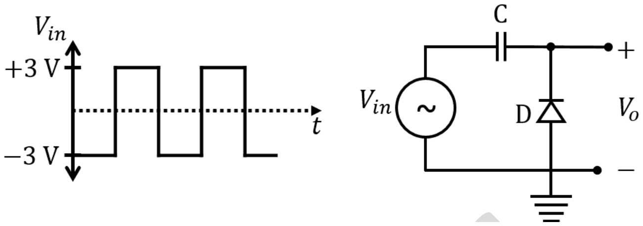
The symbols C, D, \(V_{in}\) and \(V_{0}\) shown in the figure denote capacitor, ideal diode, input voltage and output voltage, respectively.

Input: a square wave between +3 V and -3 V. Circuit: Vin in series with capacitor C to the output terminal; diode D from ground to the output, its anode at ground and cathode at the output

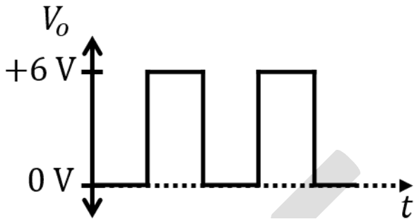
Which one of the following output waveforms \((V_{0})\) is correct for the given input waveform \((V_{in})\)?

Exam Year(s)

GATE Physics - 2024,

Answer: A

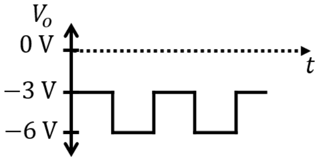
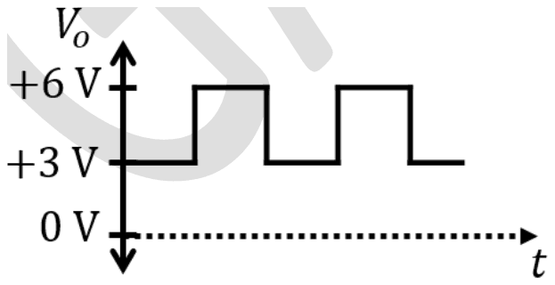
The output is a square wave between 0 V and +6 V (A).

This is a positive clamper. The diode runs from ground (anode) to the output (cathode), so it conducts whenever the output tries to go below 0 V. During the -3 V half of the input the diode conducts and the capacitor charges to 3 V, with its output side 3 V above its input side. Afterwards the diode stays off and the capacitor simply adds 3 V to the input:

\[ \begin{aligned} V_{0} &= V_{in} + 3\ \text{V} \\ -3\ \text{V} &\to 0\ \text{V}, \quad +3\ \text{V} \to +6\ \text{V} \end{aligned} \]

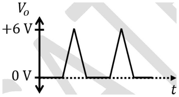
The shape of the input is preserved, so triangular pulses (B) are wrong. A wave between +3 V and +6 V (C) has the wrong shift and amplitude, and a wave between -3 V and -6 V (D) is what a clamper with the diode reversed would give, and with a halved swing.

Please log in or register to report this question.
114.

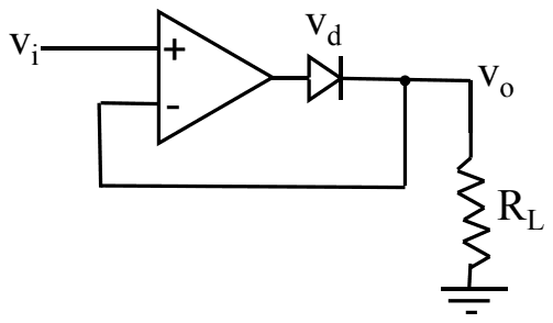
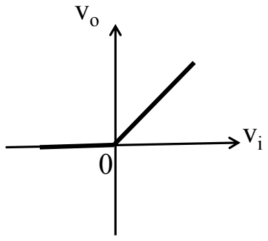
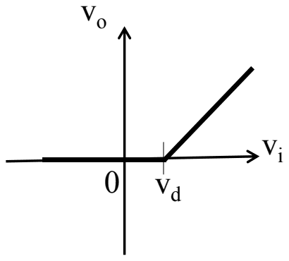
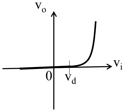
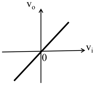
Which one of the following graphs shows the correct variation of vo with vi? Here, vd is the voltage drop across the diode and the Op-Amp is assumed to be ideal.

Op-amp with input vi at the non-inverting input; its output drives a diode whose cathode is the output vo across load RL to ground, and vo is fed back to the inverting input

Exam Year(s)

IIT JAM - 2018,

Answer: A

The correct graph is (A): \(v_{o} = 0\) for negative \(v_{i}\) and \(v_{o} = v_{i}\) for positive \(v_{i}\).

The circuit is a precision (super) diode. For \(v_{i} \gt 0\) the op-amp output rises until the diode conducts; the feedback taken from \(v_{o}\) then forces \(v_{o} = v_{i}\), and the op-amp output simply sits \(v_{d}\) higher to cover the diode drop. For \(v_{i} \lt 0\) the op-amp output swings negative, the diode is reverse biased, and \(R_{L}\) pulls \(v_{o}\) to 0.

Graph (B), with a threshold at \(v_{d}\), and graph (C), with the exponential diode curve, describe an ordinary diode without the op-amp; the feedback removes the diode drop entirely. Graph (D) is a plain follower with no rectification.

Please log in or register to report this question.
Loading…
Tags: Diode Circuits and Applications Questions and Answers || Diode Circuits and Applications MCQ Questions and Answers || Diode Circuits and Applications GK Questions and Answers || Diode Circuits and Applications GK MCQ Questions || Diode Circuits and Applications Multiple Choice Questions and Answers || Diode Circuits and Applications GK || GK on Diode Circuits and Applications || Analog Electronics Questions and Answers || Analog Electronics MCQ Questions and Answers || Analog Electronics GK Questions and Answers || GK on Analog Electronics