
Machine-translated by Google. Questions are authored in English.
Top

Diode Circuits and Applications Questions and Answers

131.

A full wave rectifier supplies DC voltage to a load resistance of 2 k\(\Omega\). The AC voltage applied to the diodes is 300-0-300 Volts rms. If the diode voltage drop is neglected, the average DC voltage across the load is nearly :

Exam Year(s)

MH SET - 2020, SET Exam - 2020,

Answer: B

The average DC voltage is nearly 270 Volts.

With a 300-0-300 V centre-tapped transformer, each diode is fed by 300 V rms, whose peak is \(V_{m} = 300\sqrt{2} = 424\) V. A full-wave rectifier's average output is \(2V_{m}/\pi\):

\[ \begin{aligned} V_{dc} &= \frac{2V_{m}}{\pi} = \frac{2 \times 424.3}{3.1416} \\ &\approx 270\ \text{V} \end{aligned} \]

That is 0.9 times the rms value. 300 V confuses rms with average, 150 V is half the rms value (the half-wave average would be \(V_{m}/\pi = 135\) V), and the load resistance does not affect the average voltage when diode drops are neglected.

Please log in or register to report this question.
132.

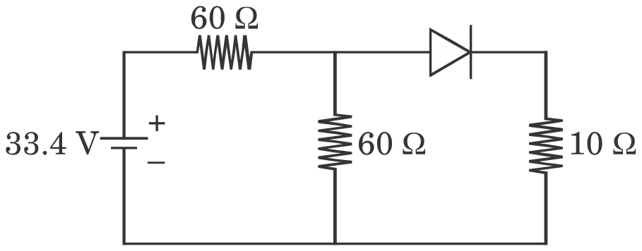
In the following circuit, the diode current flows through the resistance 10 \(\Omega\) :

33.4 V battery feeding a 60 ohm series resistor, then a 60 ohm resistor to ground, in parallel with a forward-biased diode in series with a 10 ohm resistor

If the voltage drop across the diode is 0.7 Volt, then the diode used should have minimum power rating nearly :

Exam Year(s)

MH SET - 2020, SET Exam - 2020,

Answer: C

The diode needs a minimum rating of about 280 mW.

Replace the 33.4 V source with its two 60 \(\Omega\) resistors by a Thevenin equivalent seen by the diode branch:

\[ \begin{aligned} V_{TH} &= 33.4 \times \frac{60}{120} = 16.7\ \text{V} \\ R_{TH} &= 60 \parallel 60 = 30\ \Omega \\ I &= \frac{16.7 - 0.7}{30 + 10} = 0.4\ \text{A} \\ P_{D} &= 0.7 \times 0.4 = 0.28\ \text{W} \end{aligned} \]

The diode dissipates its forward drop times its current, 280 mW, so it must be rated for at least that. 240 mW and 180 mW would underrate it, and 350 mW, while safe, is not the minimum.

Please log in or register to report this question.

133.

A Zener diode when used in voltage stabilisation circuits is biased in :

Exam Year(s)

MH SET - 2021, SET Exam - 2021,

Answer: B

The Zener diode is biased in the reverse-breakdown region.

In breakdown the voltage across a Zener diode stays almost constant at VZ over a wide range of current. Placed in parallel with the load, with a series resistor to drop the excess voltage, it therefore holds the load voltage steady while the input or the load current changes.

Below breakdown a reverse-biased diode passes almost no current and does not regulate. In forward bias it behaves like an ordinary diode with only about 0.7 V across it, and 'constant current mode' is not how a Zener stabiliser works.

Please log in or register to report this question.

134.

Match List I with List II and select the correct answer using the codes given below :

List IList II
(a) BJT(i) High β
(b) Tunnel diode(ii) Voltage regulator
(c) Zener diode(iii) Heavily doped diode
(d) MOSFET(iv) High input impedance

Exam Year(s)

MH SET - 2023, SET Exam - 2023,

Answer: B

The correct matching is a-i, b-iii, c-ii, d-iv.

  • A BJT is characterised by its current gain, a high β (i).
  • A tunnel diode is very heavily doped, so its depletion layer is thin enough for electrons to tunnel through (iii).
  • A Zener diode, operated in reverse breakdown, holds a nearly constant voltage and is used as a voltage regulator (ii).
  • A MOSFET has an insulated gate, so it draws almost no gate current and has a very high input impedance (iv).

The other codes swap these, for example making the tunnel diode a voltage regulator or giving the BJT the high input impedance that belongs to the MOSFET.

Please log in or register to report this question.

135.

For the following diode circuit, the voltage drop across each diode is 0.7 V. The current flowing through the resistor R is .............

A +10.1 V supply connected through R = 1.0 kilohm to three diodes in series, all forward biased, to ground

Exam Year(s)

MH SET - 2023, SET Exam - 2023,

Answer: C

The current is +8 mA.

The three diodes are in series and forward biased, so together they drop 3 × 0.7 = 2.1 V. The rest of the supply appears across R:

\[ \begin{aligned} I &= \frac{10.1 - 3(0.7)}{1.0\ \text{k}\Omega} \\ &= \frac{8.0\ \text{V}}{1.0\ \text{k}\Omega} = 8\ \text{mA} \end{aligned} \]

flowing from the positive supply down through R and the diodes, so positive in the direction shown. 10.1 mA ignores the diode drops, and the negative values would mean current flowing against the forward direction of the diodes, which they would block.

Please log in or register to report this question.

136.

What is the purpose of connecting a resistor in series with a Zener diode in a voltage regulator circuit ?

Exam Year(s)

MH SET - 2024, SET Exam - 2024,

Answer: B

The resistor is there to limit the current, which is what the keyed option, 'To limit the forward bias current', is getting at.

In a shunt Zener regulator the diode is reverse biased in breakdown, and its voltage stays almost constant over a wide range of current. The series resistor \(R_{S}\) drops the difference between the input and the Zener voltage, \(I = (V_{in} - V_{Z})/R_{S}\), and so keeps the Zener current within its rating as the input or the load changes. Without it the diode would draw destructive current. Strictly, the current it limits is the reverse breakdown current, so the option's word 'forward' is loose; it is still the only option about limiting current.

The breakdown voltage is fixed by the diode's doping, not by an external resistor, the resistor does not reduce the regulated reverse voltage, and mechanical stability has nothing to do with it.

Please log in or register to report this question.

137.

What is the main disadvantage of half-wave rectifier compared to full wave rectifier ?

Exam Year(s)

MH SET - 2024, SET Exam - 2024,

Answer: B

The main disadvantage of the half-wave rectifier is its lower efficiency.

A half-wave rectifier passes only one half-cycle of the input, so the theoretical maximum rectification efficiency is about 40.6%, against 81.2% for a full-wave rectifier. Its ripple factor is also much higher (1.21 against 0.48), and the DC current through the transformer secondary tends to saturate the core, lowering the transformer utilisation factor.

It is the cheaper and simpler circuit (one diode, no centre tap), so 'higher cost' and 'more complex circuitry' describe the full-wave rectifier, not the half-wave one. Its lower average output follows from the same loss of a half-cycle, but the standard comparison names efficiency as the defining drawback.

Please log in or register to report this question.

138.

A sinusoidal input voltage Vin = V0 sin ωt of frequency ω is given as an input to the following circuit. If Vm is the peak value of the input voltage, the output voltage Vout is :

Capacitor C1 in series from the input to a node; diode D1 from that node to the common line, its anode at the node; diode D2 in series between the node and the output, its cathode at the node; capacitor C2 across the output; C1 much larger than C2

Exam Year(s)

MH SET - 2024, SET Exam - 2024,

Answer: C

The output is 2 Vm.

The circuit is a half-wave voltage doubler: a clamper (C1 with D1) followed by a peak detector (D2 with C2). On one half-cycle D1 conducts and charges C1 to the peak Vm. On the other half-cycle the input and the charge on C1 add, so D2 charges C2 to twice the peak. With the diode directions shown the output is negative, of magnitude 2Vm, and it is a DC level, not a sine wave.

The options with sin ωt describe AC outputs, which a rectifier-capacitor circuit does not give once charged. \(\sqrt{2}V_{m}\) confuses peak and rms values.

Please log in or register to report this question.

139.

A barrier potential of a P-N junction depends on :

I. Type of semiconductor
II. Concentration of doping element
III. Temperature

Exam Year(s)

MH SET - 2025, SET Exam - 2025,

Answer: D

The barrier potential depends on I, II and III.

The built-in potential of a P-N junction is

\[ V_{0} = \frac{k_{B}T}{e}\ln\frac{N_{A}N_{D}}{n_{i}^{2}} \]

  • Type of semiconductor: the material fixes the band gap and so \(n_{i}\); silicon junctions have a barrier near 0.7 V, germanium near 0.3 V.
  • Doping: \(N_{A}\) and \(N_{D}\) appear directly in the logarithm.
  • Temperature: \(T\) appears in front, and \(n_{i}\) rises steeply with \(T\), so the barrier falls by roughly 2 mV per kelvin.

Any option leaving out one of the three is incomplete.

Please log in or register to report this question.

140.

The current 'I' supplied by the power supply in the given circuit is ...............

Circuit: a 5 V cell in series with a 20 ohm resistor feeds two parallel branches, the top a 50 ohm resistor with a diode pointing left and the middle a diode pointing right, which rejoin and return through a 30 ohm resistor

Exam Year(s)

MH SET - 2025, SET Exam - 2025,

Answer: C

The current is 0.1 A.

Conventional current leaves the positive (left) plate of the cell, passes the 20 Ω resistor and reaches the left junction. There it meets two diodes. The middle diode points from left to right, so it is forward biased and, taken as ideal, acts as a short. The top diode points from right to left, so it is reverse biased and blocks its branch, 50 Ω resistor and all.

The current therefore flows through the middle diode and the 30 Ω resistor back to the cell:

\[ \begin{aligned} I &= \frac{5\ \text{V}}{20\ \Omega + 30\ \Omega} \\ &= 0.1\ \text{A} \end{aligned} \]

0.05 A is what one gets by sending the current through the 50 Ω branch as well (5/100), which the reversed top diode does not allow. 1 mA and 5 mA are far too small for a 5 V source driving 50 Ω.

Please log in or register to report this question.

Loading…
Tags: Diode Circuits and Applications Questions and Answers || Diode Circuits and Applications MCQ Questions and Answers || Diode Circuits and Applications GK Questions and Answers || Diode Circuits and Applications GK MCQ Questions || Diode Circuits and Applications Multiple Choice Questions and Answers || Diode Circuits and Applications GK || GK on Diode Circuits and Applications || Analog Electronics Questions and Answers || Analog Electronics MCQ Questions and Answers || Analog Electronics GK Questions and Answers || GK on Analog Electronics