
Machine-translated by Google. Questions are authored in English.
Top

Combinational Logic Circuits Questions and Answers

1.

For a full-scale voltage of \(0 - 3\) V, the resolution of the 4-bit ADC is ______.

Exam Year(s)

DSSSB AE - 2023,

Answer: B

The resolution (the size of one step) of an n-bit ADC is the full scale range divided by \(2^n - 1\) steps.


\[ \begin{aligned} \text{Resolution} = \frac{3\ \text{V}}{2^4 - 1} \\ &= \frac{3}{15} = 0.2\ \text{V} = 200\ \text{mV} \end{aligned} \]


Dividing by 16 instead of 15 would give 187.5 mV, which is not offered, so 200 mV is the intended answer. The values 100, 300 and 400 mV would be 3 V divided by 30, 10 and 7.5, which do not correspond to a 4-bit converter. The answer is option B.

Please log in or register to report this question.

2.

What is the value of analogue output voltage Vo, for an N-bit straight binary digital to analogue converter, for the input 0010? The value of proportionality factor K is 1.

Exam Year(s)

DSSSB AE - 2023,

Answer: C

For an N bit straight binary digital to analogue converter the output voltage is the proportionality factor times the decimal value of the binary input.


\[ V_o = K \times (\text{decimal value of input}) \]


The binary input 0010 is 2 in decimal (the bit with weight \(2^1\) is set), and \(K = 1\), so


\[ V_o = 1 \times 2 = 2\ \text{V} \]


The value 1 would be for the input 0001, and 3 for 0011, and 0 for 0000. The answer is 2, option C.

Please log in or register to report this question.
3.

The "carry look ripple delay" is eliminated in :

Exam Year(s)

MH SET - 2018, SET Exam - 2018,

Answer: B

The carry ripple delay is eliminated in the carry-look-ahead adder circuit.

In a ripple-carry parallel adder each full adder must wait for the carry from the stage below, so the delay grows with the number of bits. A carry-look-ahead adder computes generate \(G_{i} = A_{i}B_{i}\) and propagate \(P_{i} = A_{i} \oplus B_{i}\) for each bit and then forms every carry directly from them and the input carry:

\[ C_{i+1} = G_{i} + P_{i}C_{i} \]

expanded so that all carries appear after a fixed number of gate delays. An ordinary parallel adder is the ripple-carry circuit that has the delay, and a single full adder or half adder (printed 'Haff-adder') handles one bit and does nothing about ripple.

Please log in or register to report this question.

4.

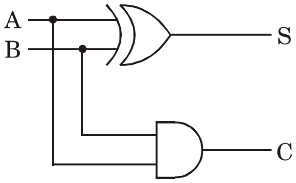
The correct circuit of a Half Adder is :

Exam Year(s)

MH SET - 2019, SET Exam - 2019,

Answer: B

The correct half adder is circuit (B): an XOR gate gives the sum S and an AND gate gives the carry C.

A half adder adds two single bits A and B. The truth table is 0+0 = 00, 0+1 = 01, 1+0 = 01 and 1+1 = 10, written as carry and sum. The sum bit is 1 only when exactly one input is 1, which is A XOR B. The carry bit is 1 only when both inputs are 1, which is A AND B:

\[ S = A \oplus B \]

\[ C = A \cdot B \]

Circuit (A) swaps the two gates, so it gives the wrong sum and carry. Circuit (C) uses an OR gate for the sum, which gives 1 for 1+1 where the sum should be 0. Circuit (D) uses NAND and NOR gates, which are the complements of AND and OR, so it is not an adder either.

Please log in or register to report this question.

5.

Match the List-I with List-II and select the correct answer using the codes given below the lists :

List-IList-II
(a) ALU(i) EXOR-Gate
(b) Parity checker(ii) Full adder
(c) Shift register(iii) MOS Transistor
(d) DRAM(iv) DFF

Exam Year(s)

MH SET - 2019, SET Exam - 2019,

Answer: D

The correct matching is a-ii, b-i, c-iv, d-iii.

  • (a) An ALU performs addition with full adders (ii).
  • (b) A parity checker is built from EXOR gates, whose output reveals an odd number of 1s (i).
  • (c) A shift register is a chain of D flip-flops (iv).
  • (d) A DRAM cell stores a bit as charge on a capacitor accessed by one MOS transistor (iii).

Each other code gives the EXOR gate, the D flip-flop or the MOS transistor to the wrong block.

Please log in or register to report this question.

Loading…
Tags: Combinational Logic Circuits Questions and Answers || Combinational Logic Circuits MCQ Questions and Answers || Combinational Logic Circuits GK Questions and Answers || Combinational Logic Circuits GK MCQ Questions || Combinational Logic Circuits Multiple Choice Questions and Answers || Combinational Logic Circuits GK || GK on Combinational Logic Circuits || Digital Electronics Questions and Answers || Digital Electronics MCQ Questions and Answers || Digital Electronics GK Questions and Answers || GK on Digital Electronics