Machine-translated by Google. Questions are authored in English.
Top

Logic Gates Questions and Answers

1.

Identify the gate shown in the following figure:
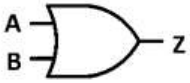
Logic gate symbol with two inputs A and B and one output Z, drawn with a curved back and a pointed front and no inversion bubble

Exam Year(s)

DSSSB AE - 2023,

Answer: B

The symbol has a curved back edge and a pointed front, and the output has no small circle (bubble) on it. That is the OR gate symbol: the output is high when either input is high. An AND gate has a flat back, a NAND gate is an AND with a bubble, and a NOT gate is a triangle with a bubble, drawn with one input. The answer is OR, option B.

Please log in or register to report this question.
2.

A two-input logic gate gives 'High' output only when either of the two inputs is high. For all other logics, it gives 'Low' output. Which is the gate?

Exam Year(s)

DSSSB AE - 2023,

Answer: D

The gate gives a high output only when exactly one of the two inputs is high, and a low output when both are low and also when both are high. That is the exclusive OR (XOR) gate, with the truth table 00 gives 0, 01 gives 1, 10 gives 1, 11 gives 0.


An ordinary OR gate gives a high output also when both inputs are high, so it does not fit the word 'only'. A NAND gate gives low only when both inputs are high, and a NOR gate gives high only when both are low. The answer is XOR, option D.

Please log in or register to report this question.
3.

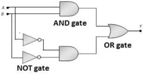
In the given logic diagram, the input A = 1, B = 0. What will be the output Y?

Logic diagram: inputs A and B feed an AND gate at the top, and through two NOT gates into a second AND gate at the bottom; the two AND gate outputs feed an OR gate with output Y

Exam Year(s)

DSSSB AE - 2023,

Answer: A

Trace the two branches of the diagram with \(A = 1\) and \(B = 0\). The top AND gate has the inputs A and B directly, so its output is \(A \cdot B = 1 \cdot 0 = 0\).


The bottom AND gate gets the inputs through the NOT gates, so its inputs are \(\bar{A} = 0\) and \(\bar{B} = 1\), and its output is \(0 \cdot 1 = 0\).


\[ Y = 0 + 0 = 0 \]


The OR gate gives 0 only when both of its inputs are 0, which is the case. Options 2 and 3 are not possible as the output of a logic gate, which is only 0 or 1, and 1 would need one of the AND outputs to be 1. The answer is 0, option A.

Please log in or register to report this question.
4.

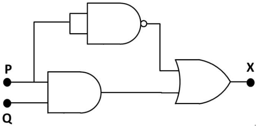
Which one of the following options is CORRECT for the given logic circuit?

P feeds both inputs of a NAND gate and one input of an AND gate whose other input is Q; the NAND and AND outputs feed an OR gate whose output is X

Exam Year(s)

GATE Physics - 2023,

Answer: D

The correct option is P = 0, Q = 0; X = 1.

Both inputs of the NAND gate are tied to P, so it acts as an inverter and outputs \(\overline{P}\). The AND gate outputs \(PQ\). The OR gate combines them:

\[ X = \overline{P} + PQ = \overline{P} + Q \]

Check each option: with P = 0, Q = 0, \(X = 1 + 0 = 1\), as stated. With P = 1, Q = 1, \(X = 0 + 1 = 1\), not 0. With P = 1, Q = 0, \(X = 0 + 0 = 0\), not 1. With P = 0, Q = 1, \(X = 1\), not 0. So only the last option is consistent with the circuit.

Please log in or register to report this question.
5.

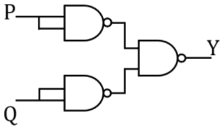
Consider the following circuit:

Logic circuit: P drives a two-input NAND gate with both inputs tied together, Q drives another such NAND gate, and their outputs feed a third NAND gate whose output is Y

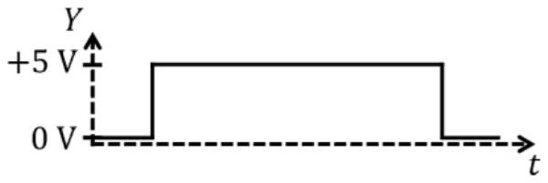
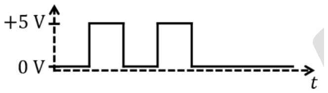
Suppose the input signal P is

Signal P: two pulses from 0 V to +5 V early in the time window, then 0 V

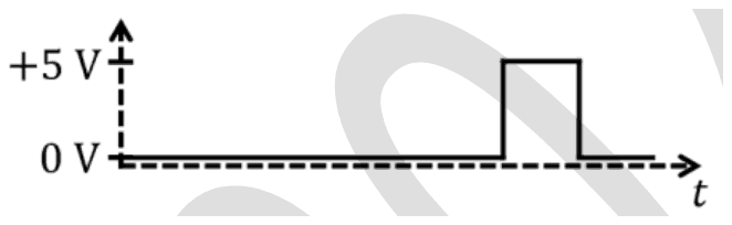
and the input signal Q is

Signal Q: 0 V until one pulse to +5 V later in the time window, after both pulses of P

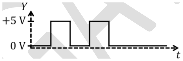
Which one of the following output signals is correct?

Exam Year(s)

GATE Physics - 2024,

Answer: A

The output is three pulses (A).

A NAND gate with both inputs tied together is an inverter, so the first two gates give P′ and Q′. The final NAND gives

\[ Y = (P' \cdot Q')' = P + Q \]

by De Morgan's law. So Y is high whenever P or Q is high. P has two pulses early on and Q one pulse later, at a time when P is low, so Y shows all three pulses.

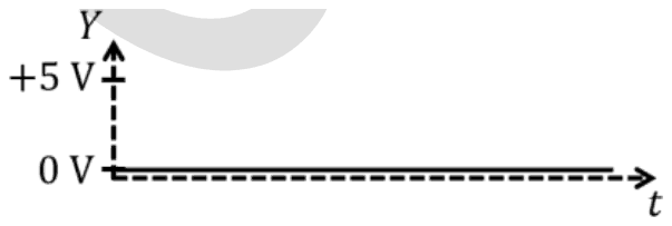
Two pulses (B) would be P alone, ignoring Q. A flat zero (C) is P AND Q, which is never high since the pulses do not overlap. One long pulse (D) does not follow from any combination of these inputs.

Please log in or register to report this question.
6.

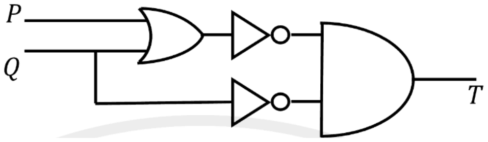
A logic gate circuit is shown in the figure below. The correct combination for the input \((P, Q)\) for which the output \(T = 1\) is

Logic circuit: inputs P and Q feed an OR gate whose output goes through a NOT gate; Q also goes through a second NOT gate; the two NOT outputs feed an AND gate with output T

Exam Year(s)

GATE Physics - 2025,

Answer: A

The output is 1 only for \((P, Q) = (0, 0)\).

The upper branch gives \(\overline{P + Q}\) (OR followed by NOT, a NOR), and the lower branch gives \(\overline{Q}\). The AND gate combines them:

\[ \begin{aligned} T &= \overline{P + Q} \cdot \overline{Q} \\ &= \overline{P}\,\overline{Q} \cdot \overline{Q} = \overline{P}\,\overline{Q} \end{aligned} \]

So \(T = 1\) only when both inputs are 0. For (0,1), (1,1) and (1,0) at least one input is 1, the NOR output is 0, and the AND gate gives 0.

Please log in or register to report this question.

7.

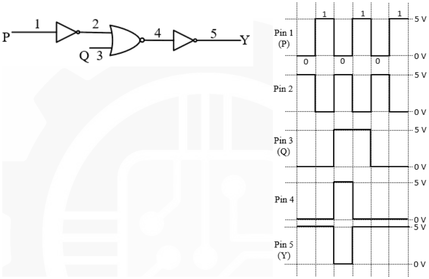
Considering the circuit and the associated signals measured at different pins (numbered as 1, 2, 3, 4, 5) shown in the figure, the correct option is

Circuit P to NOT gate (pin 2), pins 2 and 3 (Q) to NOR gate (pin 4), pin 4 to NOT gate (pin 5, Y), with the voltage waveforms at pins 1 to 5 over six equal intervals

Interval123456
Pin 1 (P)010101
Pin 2101010
Pin 3 (Q)001100
Pin 4001000
Pin 5 (Y)110111

Exam Year(s)

GATE Physics - 2026,

Answer: B

The NOR gate is faulty.

Check each gate against its own inputs. The first NOT gate is fine: pin 2 (1, 0, 1, 0, 1, 0) is the inverse of pin 1 (0, 1, 0, 1, 0, 1). The output NOT gate is fine: pin 5 (1, 1, 0, 1, 1, 1) is the inverse of pin 4 (0, 0, 1, 0, 0, 0).

A working NOR gate gives 1 only when both inputs are 0. With pin 2 = 1, 0, 1, 0, 1, 0 and pin 3 = 0, 0, 1, 1, 0, 0, both are 0 in intervals 2 and 6, so pin 4 should read 0, 1, 0, 0, 0, 1. It actually reads 0, 0, 1, 0, 0, 0, high only when both inputs are 1, which is AND behaviour. So the NOR gate alone is at fault, and the options blaming either NOT gate, or both the NOR and the output NOT gate, are ruled out by the checks above.

Please log in or register to report this question.
8.

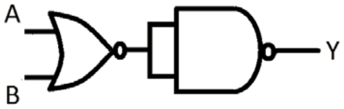
The logic operation (OR, AND, NOR or NAND) carried out by following circuit is

Inputs A and B go to a NOR gate; the NOR output is connected to both inputs of a NAND gate, whose output is Y

Exam Year(s)

IIT JAM - 2018,

Answer: C

The circuit performs the OR operation.

The NOR gate gives \(\overline{A + B}\). A NAND gate with both inputs tied together acts as an inverter, since \(\overline{X \cdot X} = \overline{X}\). So

\[ Y = \overline{\overline{A + B}} = A + B \]

which is OR. NOR would be the output of the first gate alone, without the inverting NAND. AND and NAND would need the inputs to be combined by an AND-type gate first, but here they enter a NOR gate.

Please log in or register to report this question.
Loading…

Other Subjects

Tags: Logic Gates Questions and Answers || Logic Gates MCQ Questions and Answers || Logic Gates GK Questions and Answers || Logic Gates GK MCQ Questions || Logic Gates Multiple Choice Questions and Answers || Logic Gates GK || GK on Logic Gates || Digital Electronics Questions and Answers || Digital Electronics MCQ Questions and Answers || Digital Electronics GK Questions and Answers || GK on Digital Electronics