Machine-translated by Google. Questions are authored in English.
Top

Atomic Structure and Bonding Questions and Answers

11.

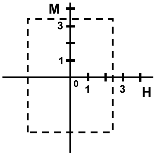
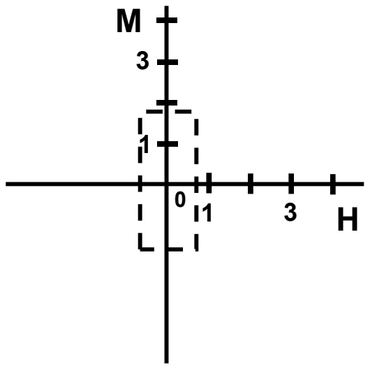
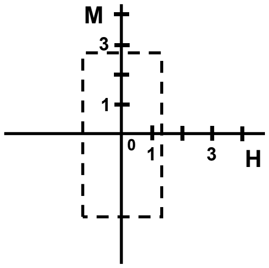
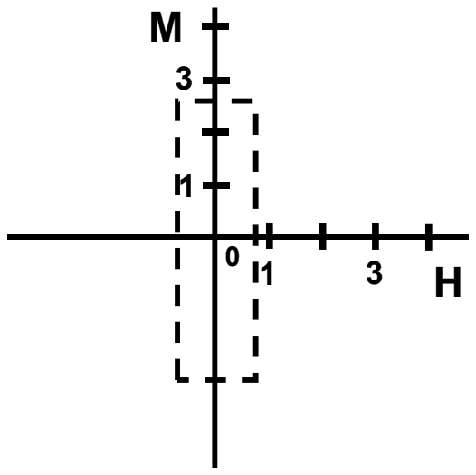
The magnetization (M) - magnetic field (H) curves for four different materials are given below. Which one of these materials is most suitable for use as a permanent magnet?
Exam Year(s)

GATE XE - 2023,

Answer: C

The material best suited to a permanent magnet is (C).

A permanent magnet must keep a large magnetization when the field is removed (high remanence, where the loop crosses the M axis) and must resist being demagnetized (high coercivity, where it crosses the H axis). Such hard magnetic materials have broad, square loops enclosing a large area.

Loop (C) is the widest, crossing the H axis at about 2.5 units, and also the tallest, so it has both the largest coercivity and the largest remanence. Loops (A), (B) and (D) are progressively narrower: a few tenths to just over one unit of field would demagnetize them. Narrow loops suit soft magnetic materials, such as transformer cores, where low hysteresis loss matters.

Please log in or register to report this question.
12.

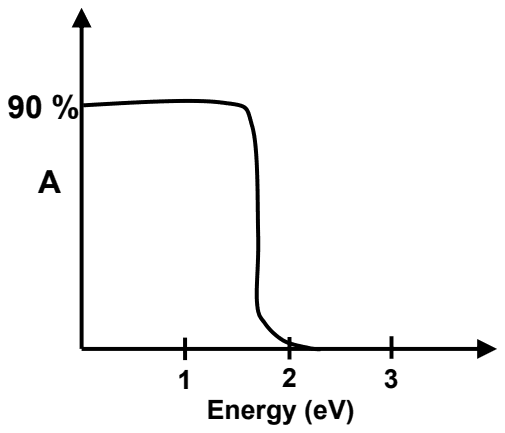
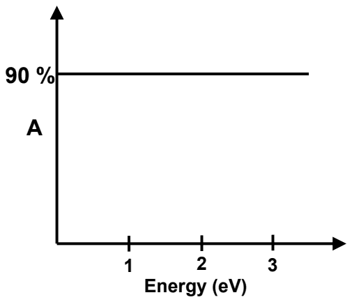
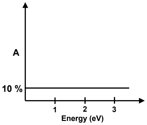
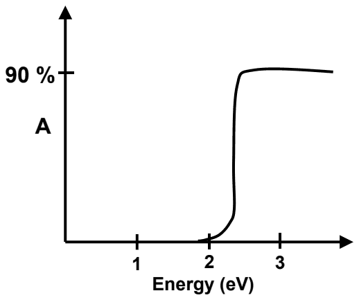
The band gap of a semiconducting material is ~ 2 eV. Which one of the following absorption (A) vs. energy (in eV) curves is correct?

Exam Year(s)

GATE XE - 2023,

Answer: D

The correct curve is (D).

A photon can be absorbed by exciting an electron across the band gap only if its energy is at least \(E_{g}\). For \(E_{g} \approx 2\) eV, light below about 2 eV passes through with little absorption, and above about 2 eV absorption rises steeply to a high value. That is the step up near 2 eV in curve (D).

Curve (A) is reversed, absorbing low-energy photons and transmitting high-energy ones. The flat curves (B) and (C) show no absorption edge at all, which is how a metal (strong absorption at all energies) or a wide-gap insulator in this range might behave, not a 2 eV semiconductor.

Please log in or register to report this question.
13.

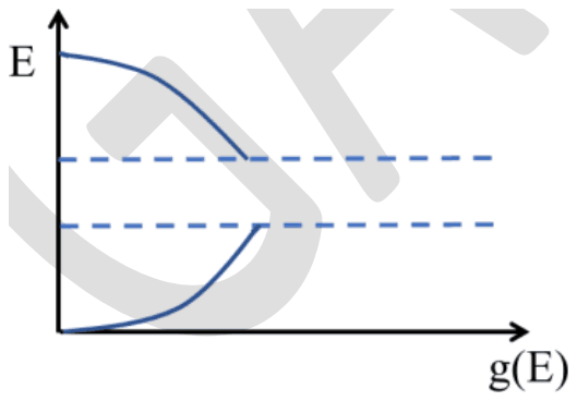
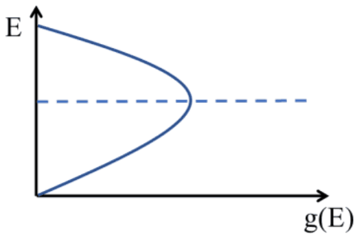
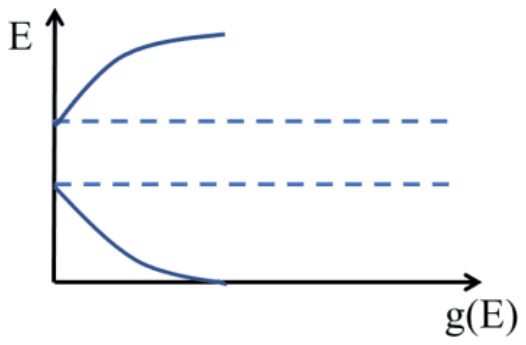
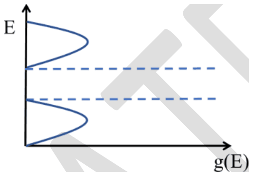
Which one of the following figures corresponds to the density of states g(E) of a typical intrinsic semiconductor? (E represents the energy level of a charge carrier)

Exam Year(s)

GATE XE - 2024,

Answer: C

The correct figure is (C).

An intrinsic semiconductor has a filled valence band and an empty conduction band separated by a gap with no allowed states, so the plot must show two bands with a gap. Near each band edge the density of states is proportional to \(\sqrt{E - E_{edge}}\), so \(E - E_{edge} \propto g^{2}\): plotted with E up and g(E) across, each curve leaves the edge with a horizontal tangent and then bends towards the vertical. Each band is finite, so g(E) rises to a maximum and returns to zero at the other edge, which gives the two separate lobes of (C).

(A) has one continuous band and no gap (a metal-like picture). (D) shows the two bands overlapping, which has no gap. (B) does have a gap, but its curves leave the axis steeply (the wrong curvature for a square-root edge) and have no upper limit to the band, so it is not the usual picture.

Please log in or register to report this question.
14.

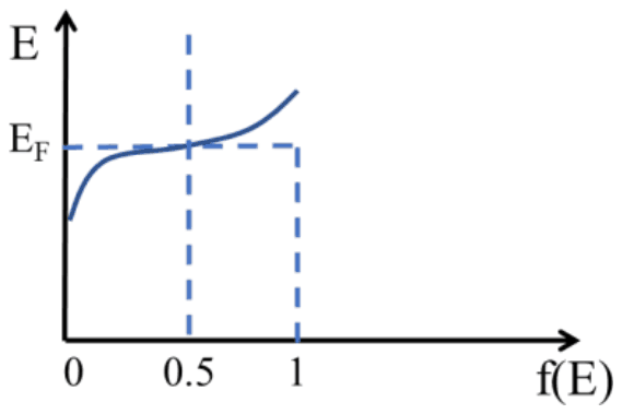
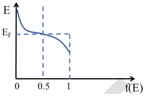
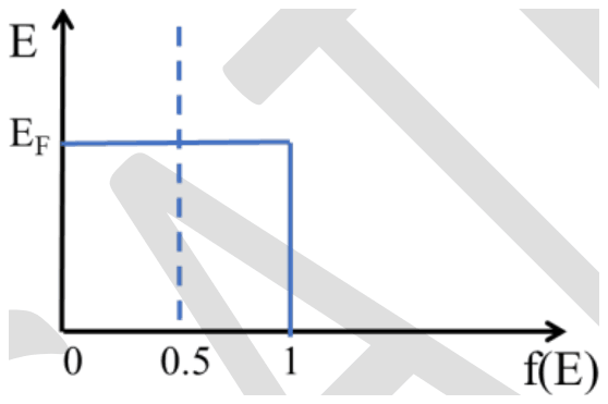
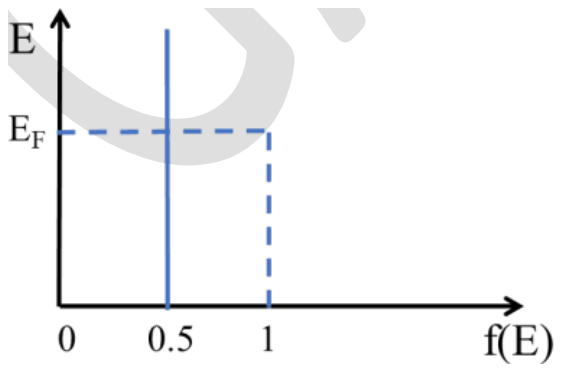
Which one of the following curves best represents the E vs. f(E) behavior of the hot end of a metal rod demonstrating Seebeck Effect? ( f(E) is the probability of electron occupancy at an energy state E ; EF is the Fermi energy)

Exam Year(s)

GATE XE - 2024,

Answer: B

The correct curve is (B).

Electron occupancy follows the Fermi-Dirac function \(f(E) = 1/(1 + e^{(E - E_F)/kT})\). It is close to 1 well below \(E_F\), close to 0 well above, and exactly 0.5 at \(E_F\). At the hot end of the rod, T is higher, so the change from 1 to 0 is spread over a wider energy range of a few kT. Plot (B) shows f falling smoothly from 1 through 0.5 at \(E_F\) towards 0 as E rises.

Plot (A) has occupancy increasing with energy, which is backwards. Plot (C) is the sharp step of absolute zero, appropriate to a cold end rather than a hot one, and (D), with f = 0.5 at every energy, is not a Fermi distribution.

Please log in or register to report this question.
15.

The unit of measurement for magnetic dipole moment of a body is

Exam Year(s)

GATE XE - 2025,

Answer: A

The unit is A m2.

A magnetic dipole moment is the current in a loop times the loop's area, \(m = IA\), so its SI unit is ampere times square metre. Equivalently, it is torque per unit flux density, N m / T, which reduces to A m2.

A m−1 is the unit of magnetic field strength H and of magnetisation (dipole moment per unit volume). Wb m−2 (tesla) is the unit of flux density B. Wb m2 is not a standard magnetic quantity.

Please log in or register to report this question.
16.

B is the magnetic flux density and Tc is the critical temperature. The Meissner effect is represented by

Exam Year(s)

GATE XE - 2025,

Answer: A

The Meissner effect is \(B = 0\) at \(T \le T_{c}\).

When a superconductor is cooled below its critical temperature in a magnetic field, it expels the magnetic flux from its interior: the flux density inside becomes zero. The material behaves as a perfect diamagnet (\(\chi = -1\)), which distinguishes a superconductor from a merely perfect conductor.

Above \(T_{c}\) the material is a normal conductor and the field penetrates, so \(B = 0\) at \(T \gt T_{c}\) is wrong, and \(B \ne 0\) below \(T_{c}\) denies the effect. \(\nabla B = 0\) is not a statement of the Meissner effect.

Please log in or register to report this question.
17.

The band gap of a material is Eg and the energy of an incident photon is Ep. Optical absorption will occur in this material if,

Exam Year(s)

GATE XE - 2026,

Answer: A

Optical absorption occurs when \(E_{g} \lt E_{p}\).

A photon is absorbed across the band gap by lifting an electron from the valence band into the conduction band, leaving a hole behind. That is possible only if the photon carries at least the band gap energy, so the photon energy must exceed (or at least equal) Eg. This is why a semiconductor is transparent to light with photon energy below its gap.

If \(E_{g} \gt E_{p}\) the photon cannot bridge the gap and passes through. Electron-hole recombination is the reverse process, which emits light (as in an LED) rather than absorbing it, and 'electron-electron recombination' is not a physical process.

Please log in or register to report this question.
Loading…
Tags: Atomic Structure and Bonding Questions and Answers || Atomic Structure and Bonding MCQ Questions and Answers || Atomic Structure and Bonding GK Questions and Answers || Atomic Structure and Bonding GK MCQ Questions || Atomic Structure and Bonding Multiple Choice Questions and Answers || Atomic Structure and Bonding GK || GK on Atomic Structure and Bonding || Materials Science Questions and Answers || Materials Science MCQ Questions and Answers || Materials Science GK Questions and Answers || GK on Materials Science