
Machine-translated by Google. Questions are authored in English.
Top

Differential Amplifiers Questions and Answers

101.

A current mirror's output impedance is \( 400 \ \mathrm{k\Omega} \) and the input devices' is \( 200 \ \mathrm{k\Omega} \). The effective load is

Answer: A

The two impedances appear in parallel at the output node:

\[ \frac{400 \times 200}{600} \approx 133 \ \mathrm{k\Omega} \]

giving about 133 kilohms. Adding them would apply to a series connection. Since the device's own output resistance now matters as much as the load's, improving only one of them yields diminishing returns - which is why a cascoded mirror is used where the highest gain is wanted.

Please log in or register to report this question.
Answer: B

Stacking a second device above each mirror transistor multiplies the output impedance by roughly that device's own gain, so the load no longer limits the stage. Offset, tail stability and common-mode range are separate matters, and the arrangement costs headroom. Applying the cascode idea to the load as well as to the input devices is how the highest-gain integrated stages are built, and both uses rest on the same mechanism.

Please log in or register to report this question.

Answer: C

A conventional cascode stacks devices and eats supply voltage, while folding the cascode to the opposite rail keeps the gain and impedance benefits with far less headroom - which matters greatly as supply voltages have fallen. It does not double the gain, still needs a tail, and does nothing for matching. A rearrangement adopted because a resource became scarce is worth recognising as such, since it explains a topology that looks needlessly complicated.

Please log in or register to report this question.
Answer: D

Digital scaling has driven supplies from fifteen volts to under two, while a transistor still needs a few hundred millivolts across it to behave properly, so the number of devices that can be stacked has fallen sharply. Thresholds have fallen rather than risen, and saturation and compliance requirements are unchanged. A constraint that tightened because of changes elsewhere in the technology is what drove folded cascodes and rail-to-rail input stages.

Please log in or register to report this question.
Answer: A

One pair works near the negative rail and a complementary pair near the positive, with the two handing over in the middle so that the inputs may reach both supplies. A cascode, a larger current and a compliant load all address other limits. The handover brings its own problem, since the offset changes as the stage switches from one pair to the other, which is a characteristic weakness worth knowing before such a device is chosen for precision work.

Please log in or register to report this question.

Answer: B

The two complementary pairs have different offsets, so as the common-mode input crosses the handover region the stage's offset shifts - a step in the transfer characteristic that limits its precision. Bandwidth, bias current direction and slew rate are affected far less. An arrangement that extends a range by switching between two circuits inherits a discontinuity where they meet, which is a general consequence worth expecting whenever such a technique is used.

Please log in or register to report this question.

107.

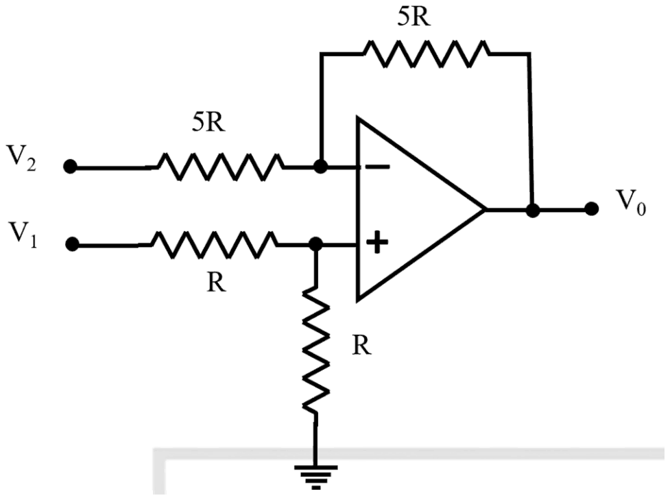
The output voltage V0 for the circuit shown in the figure is:

Op-amp: V2 goes through 5R to the inverting input, with a feedback resistor 5R from the output V0 to that input; V1 goes through R to the non-inverting input, which is also connected to ground through R

Exam Year(s)

IIT JAM - 2026,

Answer: A

The output is \(V_0 = V_1 - V_2\).

This is a difference amplifier. The non-inverting input sits on a divider of two equal resistors R, so \(V_+ = V_1/2\). By superposition, the inverting stage has gain \(-5R/5R = -1\) for \(V_2\) and the non-inverting stage has gain \(1 + 5R/5R = 2\) for \(V_+\):

\[ \begin{aligned} V_0 &= \left(1 + \frac{5R}{5R}\right)\frac{V_1}{2} - \frac{5R}{5R}V_2 \\ &= V_1 - V_2 \end{aligned} \]

\(2(V_1 - V_2)\) forgets that the divider halves \(V_1\). \(V_1 - 2V_2\) doubles the inverting gain, and \(V_2 - V_1\) has the sign of the inputs reversed.

Please log in or register to report this question.

108.

For fabrication of current mirror in an integrated circuit the following components are required :

Exam Year(s)

MH SET - 2018, SET Exam - 2018,

Answer: A

A current mirror needs two transistors.

In the basic mirror, one transistor is connected as a diode (collector tied to base, or drain to gate) and carries the reference current; the second, matched transistor shares the same base-emitter (or gate-source) voltage, so it copies that current to the output. In an IC the two devices are made side by side, so their characteristics match closely, which is exactly what the mirror relies on.

Mixing a bipolar transistor with a MOSFET destroys the matching of the control voltages. 'Super β mode' and an 'Al reflector' are not part of a current mirror at all; super-β transistors are sometimes used to improve a mirror, but they are not required.

Please log in or register to report this question.

109.

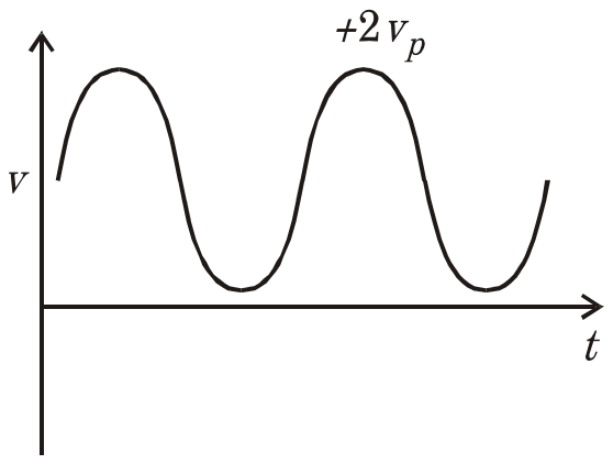
The output waveform for the following OP-Amp configuration is :

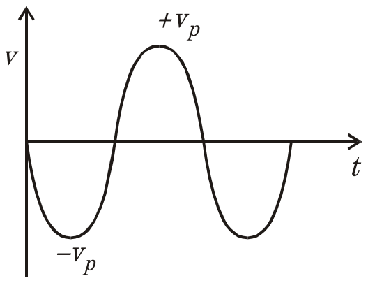
A sine input swinging between +vp and -vp feeds the inverting input of an op-amp through a series capacitor; the non-inverting input is grounded; the op-amp output drives a diode whose cathode node is fed back to the inverting input and is the output across RL

Exam Year(s)

MH SET - 2018, SET Exam - 2018,

Answer: B

The output is waveform (B), a sine wave swinging between 0 and +2vp.

The circuit is an active positive clamper. The output node is joined to the inverting input, and the capacitor sits between the source and that node. Whenever the node tries to go below 0 V, the op-amp output swings positive, the diode conducts and charges the capacitor, holding the node at 0 V. After the first negative peak the capacitor holds vp, and the diode stays off.

\[ \begin{aligned} v_{out} &= v_{in} + v_{p} \\ 0 &\le v_{out} \le 2v_{p} \end{aligned} \]

Waveform (A) is the input unchanged, (C) is a negative clamper, which needs the diode reversed, and (D) is a clipped shape that no clamper produces.

Please log in or register to report this question.

Loading…
Tags: Differential Amplifiers Questions and Answers || Differential Amplifiers MCQ Questions and Answers || Differential Amplifiers GK Questions and Answers || Differential Amplifiers GK MCQ Questions || Differential Amplifiers Multiple Choice Questions and Answers || Differential Amplifiers GK || GK on Differential Amplifiers || Analog Electronics Questions and Answers || Analog Electronics MCQ Questions and Answers || Analog Electronics GK Questions and Answers || GK on Analog Electronics